EP0430649A2 - Optisches Scheibengerät mit optimaler Aufzeichnungsvermögenseinstellung - Google Patents
Optisches Scheibengerät mit optimaler Aufzeichnungsvermögenseinstellung Download PDFInfo
- Publication number
- EP0430649A2 EP0430649A2 EP90312886A EP90312886A EP0430649A2 EP 0430649 A2 EP0430649 A2 EP 0430649A2 EP 90312886 A EP90312886 A EP 90312886A EP 90312886 A EP90312886 A EP 90312886A EP 0430649 A2 EP0430649 A2 EP 0430649A2
- Authority
- EP
- European Patent Office
- Prior art keywords
- signal
- power
- reproduced signal
- optical disk
- disk apparatus
- Prior art date
- Legal status (The legal status is an assumption and is not a legal conclusion. Google has not performed a legal analysis and makes no representation as to the accuracy of the status listed.)
- Granted
Links
Images


Classifications
-
- G—PHYSICS
- G11—INFORMATION STORAGE
- G11B—INFORMATION STORAGE BASED ON RELATIVE MOVEMENT BETWEEN RECORD CARRIER AND TRANSDUCER
- G11B7/00—Recording or reproducing by optical means, e.g. recording using a thermal beam of optical radiation by modifying optical properties or the physical structure, reproducing using an optical beam at lower power by sensing optical properties; Record carriers therefor
- G11B7/12—Heads, e.g. forming of the optical beam spot or modulation of the optical beam
- G11B7/125—Optical beam sources therefor, e.g. laser control circuitry specially adapted for optical storage devices; Modulators, e.g. means for controlling the size or intensity of optical spots or optical traces
- G11B7/126—Circuits, methods or arrangements for laser control or stabilisation
-
- G—PHYSICS
- G11—INFORMATION STORAGE
- G11B—INFORMATION STORAGE BASED ON RELATIVE MOVEMENT BETWEEN RECORD CARRIER AND TRANSDUCER
- G11B7/00—Recording or reproducing by optical means, e.g. recording using a thermal beam of optical radiation by modifying optical properties or the physical structure, reproducing using an optical beam at lower power by sensing optical properties; Record carriers therefor
- G11B7/004—Recording, reproducing or erasing methods; Read, write or erase circuits therefor
- G11B7/0045—Recording
Definitions
- This invention relates to an optical information recording apparatus which operates through the projection of a focused laser beam onto a recording medium.
- a maximum amplitude of a signal reproduced on an optical disk provides the best signal quality, and accordingly the best state of reproduced signal implies a reproduced signal with the maximum amplitude.
- the above-mentioned conventional method is also designed to determine the optimal power by detecting the operation which provides the maximum amplitude (peak-to-peak value) of the reproduced signal.
- the conventional method bases the determination of the optimal recording power on the best state of reproduced signal, and therefore it involves a problem that the determined power is not optimal for the optical disk apparatus.
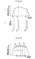
- the upper part (a) of Fig. 8 shows the peak power characteristics of a general optical disk
- the lower part (b) of Fig. 8 shows record marks on the recording medium produced by power with certain peak values.
- the term "peak power" means the above-mentioned recording power.
- the horizontal axis represents the peak-power and the vertical axis represents the amplitude or S/N of reproduced signals
- the lower part (b) of Fig. 8, indicated by 31, 32 and 33 are record marks produced by respective peak powers along the track direction indicated by the arrow. Peak power from 0 to P1 is the range of insufficient power, in which satisfactory record marks are not produced and reproduced signals have insufficient amplitudes.
- P1 is the smallest peak power to produce a satisfactory record mark.
- record marks become larger, producing greater amplitude of reproduced signals.
- the peak power exceeds P2
- the record mark becomes to have duties above 50%, and the amplitude of the reproduced signal becomes to fall due to a deficient resolution.
- the peak power further increases beyond P3, the destruction of recording medium begins and the reproduced amplitude falls sharply.
- the peak power which provides the best state of reproduced signal is P2.
- the above-mentioned peak power characteristics vary depending on the type of recording medium as shown by 34, 35 and 36 in Fig. 9.
- the recording medium 34 has the peak power P2 for the maximum (best) reproduced signal emerging nearer to the P1, the recording medium 36 has the P2 nearer to the P3, and the recording medium 35 has the P2 amid the P1 and P3.
- Fig. 9 has the same coordinates as the (a) part of Fig. 8.
- the optimal power for the optical disk apparatus is chosen at a peak power P4 which is slightly higher than the center of the power range suitable for recording and reproduction (e.g., the range between P1 and P3 on the peak power characteristics of Fig.
- the peak power which provides the best state of reproduced signal for the optical disk (recording medium), i.e., those shown by P34, P35 and P36 in Fig. 9, in not necessarily consistent with the optimal peak power P4 for the optical disk apparatus, and therefore it is difficult for the conventional optical disk apparatus, which determines the peak power based on the best recording state of reproduced signal, to find the optimal peak power for the apparatus.
- Fig. 10 shows the method of light projection for overwiting a phase-mode optical disk.
- (a) is the light modulation waveform
- (b) is a recording track before overwriting
- (c) is a recording track after overwriting.
- 40 is the bias power
- 41 is the peak power
- 42 is the crystalline state
- 43 is the amorphous state.
- Phase-mode material allows overwriting of signals based on its different optical reflectivity between the amorphous state and the crystalline state. Overwriting of signal is the capability of recording a new signal without erasing the old signal which has been recorded in the past.
- the amorphous state ad crystalline state are attained by light modulation at two laser power levels, i.e., peak power and bias power, as shown in Fig. 10. Namely, regardless of the sate of a recording track before overwriting, a portion where the peak power is applied becomes amorphous and a portion where the bias power is applied becomes crystalline, and this allows overwriting of a new signal. Although the optimal bias power and optimal peak power need to be set for apparatus with the ability of overwriting, the conventional apparatus cannot set two power levels necessary for overwriting.
- This invention is intended to overcome the foregoing prior art deficiency, and it provides an optical disk apparatus operative to overwrite user signals at the above-mentioned optimal power levels through the provision of a start circuit which initiates the optimal power setting operation, means of recording a signal while varying the peak power progressively, with the bias power being fixed, means of discriminating the quality of reproduced signal thereby to judge whether the recorded signal is useful or not, and means of determining the lower-limit peak power based on the lowest peak power among powers which have been judged to be useful by the reproduced signal quality discrimination means, and means of recording the signal while varying the bias power progressively, with the peak power being fixed, means of discriminating the quality of reproduced signal for judging whether the recorded signal is useful or not, means of determining the lower-limit bias power based on the lowest bias power among powers which have been judged to be useful by the reproduced signal quality discrimination means, and means of evaluating the optimal powers by adding a prescribed power to the lower-limit peak power and lower-limit bias power.
- the inventive optical disk apparatus is operative to overwrite user signals through the provision of bit error discrimination means as the reproduced signal quality discrimination means, which determines the lower-limit peak power and lower-limit bias power based on the lowest powers among powers by which bit error is judged to be admissible by the bit error discrimination means, and evaluates the optimal powers by adding a prescribed power to the lower-limit peak power and lower-limit bias power.
- the inventive optical disk apparatus is designed to evaluate the optimal powers each time the apparatus is powered on, the recording medium is replaced, error is detected in data recorded by the user, a certain time length has been expired since the last optimal power setting, the temperature has changed in excess of a prescribed limit, or a shock or vibration in excess of a certain magnitude is applied to the apparatus.
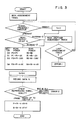
- Fig. 1 is a block diagram of the optimal power setting circuit based on an embodiment of this invention
- Fig. 2 is a flowchart showing the optimal power setting method based on an embodiment of this invention
- Fig. 3 is a flowchart showing the optimal power setting method based on another embodiment of this invention.
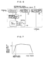
- Fig. 4 is a graph used to explain the principle of the reproduced signal quality discrimination circuit based on this invention.
- Fig. 5 is a block diagram of the reproduced signal quality discrimination circuit based on the embodiment of this invention.
- Fig. 6 is a block diagram of the reproduced signal quality discrimination circuit based on another embodiment of this invention.
- Fig. 7 is a graph used to explain the principle of the reproduced signal quality discrimination circuit of the other embodiment
- Figs. 8 and 9 are graphs of peak power characteristics used to explain the problem involved in the conventional apparatus.
- Fig. 10 is a diagram used to explain the principle of recording on a phase-mode optical disk.
- a reproduced signal quality discrimination circuit 9 is a laser power setting circuit, 11 is a drive control circuit, 12 is a reference voltage generation circuit, 13 is a comparator circuit, 14 is a bit error discrimination circuit, 15 is a PLL circuit, 16 is a data discrimination circuit, 19 is a start circuit, 40 is the bias power, and 41 is the peak power.
- Fig. 1 is a block diagram showing an embodiment of this invention for finding the optimal peak power of the optical disk apparatus.
- 1 is a photosensor which detects a signal reproduced on an optical disk
- 2 is an amplifier which amplifies the reproduced signal
- 3 is a demodulator which demodulates data in the reproduced signal and the address formed on the disk
- 4 is an unrecorded portion detector which detects the presence or absence of the reproduced signal
- 5 is a seek circuit which seeks an intended track
- 6 is a reproduced signal quality discrimination circuit
- 7 is a modulator which modulates data from a drive control circuit which will be explained later
- 8 is a recording gate control circuit
- 9 is a laser power control circuit for the laser which is used to record and/or erase a signal
- 10 is a D/A (digital to analog) converter which converts the value of laser power produced by the drive control circuit 11 made up of a microcomputer into an analog value and determines the laser power value of the laser power control circuit.
- the drive control circuit 11 is further connected with the demodulator 3, unrecorded portion detector 4, seek circuit 5, reproduced signal quality discrimination circuit 6, modulator 7, and recording gate control circuit 8, thereby controlling these circuits.
- signal recording takes place in such a manner that data produced by the drive control circuit is modulated into a recording signal by the modulator 7, recording and bias power are provided to the D/A converter 10, and the recording gate is enabled by the operation of the recording gate control circuit 8.
- Indicated by 19 is a start circuit which initiates the operation of finding the optimal peak power carried out by the above-mentioned circuits.
- the drive control circuit 11 In response to the command from the start circuit 19, the drive control circuit 11 initiates the operation for finding the optimal power. Initially, the drive control circuit 11 operates on the seek circuit 5 to seek assessment tracks. The assessment tracks are used to assess the recording state, and are located outside the user area, for example. The reproduced signal from an assessment track is fed from the photosensor 1 through the amplifier 2 to the unrecorded portion detector 4 and demodulator 3. The unrecorded portion detector 4 detects the presence or absence of an already recorded signal on the assessment track. If the signal is absent, a repetition count register N in the drive control circuit is set to zero.
- the demodulator 3 demodulates the signal, and the number of times of use of the assessment track (number of repetitions) is read from the recorded signal and its value is set in the register N. If the number of repetitions is greater than or equal to N max -10, the seek circuit 5 seeks another assessment track.
- the N max is the allowable maximum number of times of repetitive recording on an assessment track. The reason for the use of value N max -10 is based on the assumption that a same assessment track will be recorded about 10 times repeatedly in one operation to determine the optimal bias power, and the value 10 may be altered.
- a peak power setting register P in the drive control circuit is set with the reference peak power value Pr which is determined upon the design criteria, and a bias power setting register B in the drive control circuit is set with the reference bias power value Br predetermined upon the design criteria.
- Value N+1 is set to the repetition count register N, and the data in N is recorded on the assessment track at both power levels.
- the reproduced signal quality discrimination circuit 6 discriminates the signal recorded at both power levels, and in the case of a negative discrimination result for a reproduced signal, error 2 is reported to the user, and the optimal power setting operation terminates.
- setting of the optimal peak power takes place first by following the procedure described in the following.
- the peak power setting register P is re-set to a power level which is lower by dX than the currently set power level, data N+1 is set to the repetition count register N and the data in N is recorded.
- the data is subjected to discrimination by the reproduced signal quality discrimination circuit 6.
- the peak power is lowered by dx again, and the reduction of peak power is repeated until the reproduced signal quality discrimination circuit 6 produces a negative discrimination result.
- the reproduced signal quality discrimination circuit 6 has made the first negative judgement, the value in the peak power register P added by dx comes to the lower-limit peak power for the correct recording of data.
- the lower-limit peak power superimposed by the above-mentioned power margin X comes to the optimal peak power for the optical disk apparatus.
- the optimal bias power is set in the similar procedure.
- the bias power setting register B is set to a power level which is lower by dY than the currently set power level, data N+1 is set to the repetition count register, and the data is recorded.
- the data is subjected to discrimination by the reproduced signal quality discrimination circuit 6.
- the bias power is lowered by dY, and the reduction of bias power is repeated until the reproduced signal quality discrimination circuit 6 produces a negative discrimination result.
- the reproduced signal quality discrimination circuit 6 has made the first negative judgement, the value in the bias power register B added by dY comes to the lower-limit bias power for the correct recording of data.
- the power margins X and Y to be added to both lower-limit powers.
- the power margins have been determined so that the deficiency of reproduced signal does not result due to virtual peak power variation or bias power variation caused by some abnormality in the practical operation after the setting of the above-mentioned optimal.
- power levels are selected to be a little greater than half the range of upper and lower-limit powers (see Fig. 9), at which the reproduced signal quality discrimination circuit 6 makes a positive judgement for the reproduced signal.
- the reason for the threshold of half or above is that the major cause of power variation is dusts and servo out-tracking, which will result rather in a power reduction than a power increase.
- the values of power margin can be altered referring to detected values of the time length until the user actually records data, the variation in temperature, shock or vibration, etc., thereby enhancing the reliability of the power margin values.
- the present invention described above is summarized as follows.
- One of the peak power and bias power is fixed and the other is reduced gradually (by dx or dY at a time) thereby to find the lower-limit powers at which the reproduced signal quality discrimination circuit 6 makes a positive judgement for the recorded signal, and the other power vice versa, and the marginal powers (X and Y) are added to the derived lower-limit powers to determine the optimal peak power and optimal bias power.
- the optimal peak power and optimal bias power based on this invention are the optimal powers for the optical disk apparatus, and the optimal powers for the optical disk apparatus are not powers which provide the best reproduced signal, but instead which imply the peak power and bias power having power margins on both the lower and higher power sides in order to prevent defective reproduction due to a small abnormality (virtual power variation in recording and erasure).
- the inventive method sets only the peak power for a disk which is recorded without a bias power, such as a disk of write-once type.
- Conceivable conditions of starting the foregoing optimal power searching operation by the start circuit 19 are the turning-ON of the optical disk apparatus and/or the replacement of disk and/or the emergence of reproduction error in the signal recorded by the user. Because of the presence of variable performance among optical disk apparatus and among optical disks (recording medium), it is intended to correct the optimal power to match between the optical disk apparatus and optical disk that are going to be used. Other conceivable conditions are the expiration of a certain time length as detected by a timer incorporated in the start circuit 19, a temperature change in excess of a certain limit as detected by a thermal sensor incorporated in the circuit, or the application of a shock or vibration as detected by a shock/vibration sensor incorporated in the circuit.
- the optimal power searching operation may be executed on request to reset the set powers by a user or particularly a host computer executing a diagnosis on the optical disk apparatus or the optical disks.
- These schemes are intended to correct the optimal power to meet the performance at the time of use of the optical disk apparatus which has changed due to a change in the operational environment (temperature, shock or vibration, dusts, etc.).
- the correction of optimal powers are not to be executed during data are recorded by a user.
- Fig. 3 is a flowchart used to explain another embodiment of this invention.
- the arrangement of the circuit blocks used in the apparatus is identical to the first embodiment shown in Fig. 1, but the software used in the drive control circuit 11 is different.
- Fig. 3 the operation from the beginning until the finding of the assessment track is shown in Fig. 2, and its explanation is not repeated.
- the reason for setting an upper limit value of N max -2 for the number of repetitions is to use the same assessment track twice until the optimal power is found, and this value may be altered.
- an optical disk designed to record data is partitioned into sectors, and accordingly the assessment track is made up of plural sectors. These sectors are recorded at different power levels.
- the peak power and bias power of each sector is set in the following manner, for example.
- Sector 0 has its peak power P0 set to the reference peak power level Pr which is decided according to the design criteria and its bias power B0 set to the reference bias power level Br decided on the design criteria.
- Sector 1 has its powers P1 and B1 set to Pr-dX and Br-dY, respectively.
- Sector 2 has its powers P2 and 02 set to Pr-2dX and Br-2dY, respectively.
- sector m has its powers Pm and Bm set to Pr-m.dX and Br-m.dY, respectively, for recording.
- the foregoing two methods of finding the optimal power for the optical disk apparatus are both designed to find a useful lower-limit peak power and/or lower-limit bias power with the reproduced signal quality discrimination circuit 6, and thereafter to set the optimal peak power and optimal bias power for the optical disk apparatus.
- Fig. 4 is a diagram used to explain the principle of operation of the reproduced signal quality discrimination circuit 6 formed of a bit error discrimination circuit.
- the diagram shows the bit error rate (will be termed BER hereinafter) vs. peak power characteristics.
- the horizontal axis represents the peak power, and the vertical axis represents the BER.
- the peak power is increased progressively from the bottom, the BER becomes better (falls in the BER value), and in response to the detection of BER below the admissible BER value, e.g., 10 ⁇ 4 or less the reproduced signal quality discrimination circuit 6 makes a positive judgement for the reproduced signal and informs it to the drive control circuit. This peak power comes to the lower-limit peak power.
- the lower-limit peak power can easily be found. Conversely, the BER does not vary greatly at points beyond the lower-limit power, and it is difficult to find the peak power which provides the best reproduced signal.
- the virtual peak power falls down to the lower-limit power due to any of the above mentioned abnormalities. Therefore, in order to enhance the reliability of signal at the lower-limit power, the BER at the lower-limit power is measured precisely in the following manner.
- Fig. 5 shows another embodiment of the reproduced signal quality discrimination circuit 6 used in the present invention.
- Terminal 1 receives the reproduced signal from the assessment track provided by the amplifier 2, and terminal J delivers the result of judgement by the reproduced signal quality discrimination circuit 6 to the drive control circuit.
- the analog reproduced signal is compared by the comparator circuit 13 with the reference voltage Vt (voltage level half the amplitude of the reproduced signal, in general) produced by the reference voltage generation circuit 12, and the resulting binary signal is sent to the bit error judgement circuit 14.
- Vt voltage level half the amplitude of the reproduced signal, in general
- the reference voltage is switched between Vt+dVt and Vt-dVt during the process of finding the lower-limit power, and such a power that does not cause a bit error based on the comparison with both of the two reference voltages is appointed to be the lower-limit power of recording and/or bias power.
- bit errors caused by uneven amplitude of reproduced signal due to a lacking peak power or caused by the residual of erasure due to a lacking bias power can be checked more strictly, whereby the reliability of recorded signal at the lower-limit power is enhanced.
- Fig. 6 shows another embodiment of the invention which is intended to enhance the reliability of signal at the lower-limit power.
- the figure is a block diagram of another embodiment of the reproduced signal quality discrimination circuit 6. Circuit blocks identical to those of Fig. 5 are given the common reference numbers.
- the binary signal provided by the comparator is subjected to data extraction by a data extraction circuit 16 used with reference clock produced by a known PLL (phase-locked loop) circuit 15, and the extracted data are sent to the bit error judgement circuit 14.
- the reference clock is set to the clock frequency fc for data.
- the reference clock frequency is switched between fc+dfc and fc-dfc in the process of finding the lower-limit power, so that such a power that does not cause a bit error based on the data extraction at the two frequencies is appointed to be the lower-limit power of recording and/or bias power.
- bit errors caused by defective S/N due to a lacking peak power or bias power or in other words, bit errors caused by the jitter of reproduced signal (swing of the time axis of reproduced signal) can be checked more strictly, whereby the reliability of recorded signal at the lower-limit power is enhanced.
- Fig. 7 is a diagram used to explain the principle of operation of the reproduced signal quality discrimination circuit 6 formed of a reproduced signal amplitude discrimination circuit.
- the diagram shows the reproduced signal vs. peak power characteristics.
- the horizontal axis represents the peak power and the vertical axis represents the amplitude of reproduced signal.
- the reproduced signal quality discrimination circuit 6 makes a positive judgement for the reproduced signal and informs it to the drive control circuit.
- the peak power at this point comes to the lower-limit peak power.
- this invention is designed to find the lower-limit peak power and lower-limit bias power, and thereafter find the optimal power for the optical disk apparatus, and consequently the optimal power can easily be found and it becomes possible to set the optimal power definitely and uniquely.
- the optimal power found based on this invention is the optimal power for the optical disk apparatus, and even if such abnormalities as servo out-tracking and power fluctuation emerge due to an environmental change during the practical operation, the presence of a marginal power, which impedes the reproduced signal become defective, enhances the stability of the optical disk apparatus.
- this invention is designed to discriminate the signal quality at the lower-limit power more strictly than the usual manner, resulting in a higher reliability of signal at the lower-limit power.
- the optimal power can be corrected to match the optical disk apparatus and optical disk that are going to be used, or even if there arises an environmental change (temperature, shock or vibration, dusts, etc.) during the operation of the optical disk apparatus, the optimal power can be corrected to match the performance at the time of operation, whereby a reliable optical disk apparatus which is immune to the influence of environmental changes can be offered.
Landscapes
- Physics & Mathematics (AREA)
- Optics & Photonics (AREA)
- Optical Recording Or Reproduction (AREA)
- Optical Head (AREA)
Applications Claiming Priority (2)
| Application Number | Priority Date | Filing Date | Title |
|---|---|---|---|
| JP1311181A JPH03171437A (ja) | 1989-11-30 | 1989-11-30 | 信号記録方法と最適パワー設定装置 |
| JP311181/89 | 1989-11-30 |
Publications (3)
| Publication Number | Publication Date |
|---|---|
| EP0430649A2 true EP0430649A2 (de) | 1991-06-05 |
| EP0430649A3 EP0430649A3 (en) | 1991-11-06 |
| EP0430649B1 EP0430649B1 (de) | 1995-10-18 |
Family
ID=18014065
Family Applications (1)
| Application Number | Title | Priority Date | Filing Date |
|---|---|---|---|
| EP90312886A Expired - Lifetime EP0430649B1 (de) | 1989-11-30 | 1990-11-27 | Optisches Scheibengerät mit optimaler Aufzeichnungsvermögenseinstellung |
Country Status (4)
| Country | Link |
|---|---|
| US (1) | US5140580A (de) |
| EP (1) | EP0430649B1 (de) |
| JP (1) | JPH03171437A (de) |
| DE (1) | DE69023102T2 (de) |
Cited By (12)
| Publication number | Priority date | Publication date | Assignee | Title |
|---|---|---|---|---|
| EP0557584A1 (de) * | 1992-02-27 | 1993-09-01 | Pioneer Electronic Corporation | Verfahren und Vorrichtung zur Aufzeichnung von Informationen auf einer beschreibbaren optischen Platte |
| EP0642122A1 (de) * | 1993-09-03 | 1995-03-08 | Pioneer Electronic Corporation | Optische Aufzeichnungsscheibe und Aufzeichnungsgerät dafür |
| EP0599389A3 (de) * | 1992-11-20 | 1995-04-19 | Koninkl Philips Electronics Nv | Verfahren und Vorrichtung zur Aufzeichnung von Signalen auf einen Aufzeichnungsträger. |
| EP0737969A3 (de) * | 1995-04-10 | 1997-01-08 | Nippon Kogaku Kk | Optische Aufzeichnungsverfahren und optisches Aufzeichnungsgerät |
| EP0762400A1 (de) * | 1995-08-30 | 1997-03-12 | Canon Kabushiki Kaisha | Vorrichtung und Verfahren zur optischen Aufzeichnung und/oder Wiedergabe von Information |
| EP0773543A3 (de) * | 1995-11-07 | 1997-05-28 | Nikon Corporation | Optisches Aufzeichnungsverfahren zum stabilisierten Überschreiben von Daten mit Laserstrahlintensitätseinstellung |
| EP0773540A3 (de) * | 1995-11-07 | 1997-06-04 | Nikon Corporation | Stabilisiertes optisches Überschreibverfahren mit Laserstrahlintensitätseinstellung |
| EP0782134A1 (de) * | 1995-12-28 | 1997-07-02 | Nikon Corporation | Optisches Aufzeichnungsverfahren zum stabilisierten Überschreiben mit Laserstrahlintensitätseinstellung |
| EP0803866A3 (de) * | 1996-04-26 | 1998-01-21 | Fujitsu Limited | Optisches Speichergerät |
| US5726954A (en) * | 1995-04-10 | 1998-03-10 | Nikon Corporation | Optical recording method and apparatus |
| CN1069431C (zh) * | 1992-11-20 | 2001-08-08 | 皇家菲利浦电子有限公司 | 在记录载体上记录信号的方法及记录装置 |
| US6661759B1 (en) | 1999-06-18 | 2003-12-09 | Samsung Electronics Co., Ltd. | Adaptive recording method and apparatus for high-density optical recording, and control method therefor |
Families Citing this family (61)
| Publication number | Priority date | Publication date | Assignee | Title |
|---|---|---|---|---|
| US6529451B2 (en) | 1992-10-05 | 2003-03-04 | Mitsubishi Denki Kabushiki Kaisha | Optical disk and optical disk drive device |
| US7548497B2 (en) | 1992-10-05 | 2009-06-16 | Mitsubishi Denki Kabushiki Kaisha | Optical disk and optical disk drive device |
| JP2885650B2 (ja) * | 1993-11-11 | 1999-04-26 | 株式会社東芝 | ディスク再生装置 |
| JPH08509314A (ja) * | 1994-02-14 | 1996-10-01 | フィリップス エレクトロニクス ネムローゼ フェン ノートシャップ | 記録キャリヤに信号を記録する方法および記録装置 |
| US5841747A (en) * | 1995-08-22 | 1998-11-24 | Matsushita Electric Industrial Co., Ltd. | Optical disk device and method for setting recording power and erasing power |
| JPH11144255A (ja) * | 1997-11-04 | 1999-05-28 | Sony Corp | 光情報再生装置及び光情報再生方法 |
| JP2002208148A (ja) * | 2001-01-12 | 2002-07-26 | Pioneer Electronic Corp | 記録ディスクの記録済み領域及び未記録領域の境界位置検索方法及び情報記録装置 |
| US6970410B2 (en) * | 2001-01-25 | 2005-11-29 | Dphi Acquisitions, Inc. | Focus detection in a digital focus servo system |
| US6704261B2 (en) | 2001-01-25 | 2004-03-09 | Dphi Acquisitions, Inc. | Spin motor control in an optical drive |
| US6738320B2 (en) | 2001-01-25 | 2004-05-18 | Dphi Acquisitions, Inc. | System and method for moving optical pick up from current position to target position with smooth control |
| US6781929B2 (en) | 2001-01-25 | 2004-08-24 | Dphi Acquisitions, Inc. | Digital tracking servo system with multi-track seek |
| US7092322B2 (en) * | 2001-01-25 | 2006-08-15 | Dphi Acquisitions, Inc. | Calibration of focus error signal offset in a focus servo system |
| US7680004B2 (en) * | 2001-01-25 | 2010-03-16 | Dphi Acquisitions, Inc. | Digital servo system with inverse non-linearity compensation |
| US6813226B2 (en) | 2001-01-25 | 2004-11-02 | Dphi Acquisitions, Inc. | Calibration of a focus sum threshold in a focus servo system |
| US6891781B2 (en) * | 2001-01-25 | 2005-05-10 | Dphi Acquisitions, Inc. | Digital servo system with second order compensator |
| US6937543B2 (en) | 2001-01-25 | 2005-08-30 | Dphi Acquisitions, Inc. | Digital focus servo system with a sliding notch filter |
| US6898164B2 (en) * | 2001-01-25 | 2005-05-24 | Dphi Acquisitions, Inc. | Close tracking algorithm in a digital tracking servo system |
| US7023766B2 (en) | 2001-01-25 | 2006-04-04 | Dphi Acquisitions, Inc. | Flexible servicing of servo algorithms using a digital signal processor |
| US7522480B2 (en) | 2001-01-25 | 2009-04-21 | Dphi Acquisitions, Inc. | Digital tracking servo system with multi-track seek with an acceleration clamp |
| US7260031B2 (en) | 2001-01-25 | 2007-08-21 | Dphi Acquisitions, Inc. | Digital focus and tracking servo system with one-track jump |
| US7095683B2 (en) * | 2001-01-25 | 2006-08-22 | Dphi Acquisitions, Inc. | Tracking and focus digital servo system with write abort |
| US6882603B2 (en) | 2001-01-25 | 2005-04-19 | Dphi Acquisitions, Inc. | Digital tracking servo system with tracking skate detection |
| US6882601B2 (en) | 2001-01-25 | 2005-04-19 | Dphi Acquisitions, Inc. | Digital servo system with feed-forward control loops |
| US6958957B2 (en) * | 2001-01-25 | 2005-10-25 | Dphi Acquisitions, Inc. | Digital tracking and focus servo system with TES to FES crosstalk calibration |
| US6970403B2 (en) * | 2001-01-25 | 2005-11-29 | Dphi Acquisition, Inc. | Calibration of tracking error signal offset in a tracking servo system |
| US6950380B2 (en) * | 2001-01-25 | 2005-09-27 | Dphi Acquisitions, Inc. | Detector input dark current offset calibration in an optical disk drive digital servo |
| US6885619B2 (en) | 2001-01-25 | 2005-04-26 | Dphi Acquisitions, Inc. | Detector input stray light offset calibration in an optical disk drive |
| US6909676B2 (en) | 2001-01-25 | 2005-06-21 | Dphi Acquisitions, Inc. | Digital tracking servo system with multi-track seek with track zero crossing detection |
| US7593300B2 (en) | 2001-01-25 | 2009-09-22 | Dphi Acquisitions, Inc. | Digital tracking servo system with off-format detection |
| US6847597B2 (en) | 2001-01-25 | 2005-01-25 | Dphi Acquisitions, Inc. | Optical disk drive with a digital focus and tracking servo system |
| US7672199B2 (en) | 2001-01-25 | 2010-03-02 | Dphi Acquisitions, Inc. | Close focus algorithm in a digital focus servo system |
| US7196979B2 (en) | 2001-01-25 | 2007-03-27 | Dphi Acquisitions, Inc. | Calibration storage methods for a digital focus and tracking servo system with calibration |
| US6891789B2 (en) * | 2001-01-25 | 2005-05-10 | Dphi Acquisitions, Inc. | Tracking and focus servo system with automatic media type detector |
| US6965547B2 (en) * | 2001-01-25 | 2005-11-15 | Dphi Acquisitions, Inc. | Tracking and focus servo system with error signal inverse non-linearity calibration |
| US6813228B2 (en) | 2001-01-25 | 2004-11-02 | Dphi Acquisitions, Inc. | Tracking and focus servo system with direction sensor |
| US6906985B2 (en) | 2001-01-25 | 2005-06-14 | Dphi Acquisitions, Inc. | Calibration of tracking error signal gain in a tracking servo system |
| US6809995B2 (en) | 2001-01-25 | 2004-10-26 | Dphi Acquisitions, Inc. | Digital focus and tracking servo system |
| US6847596B2 (en) | 2001-01-25 | 2005-01-25 | Dphi Acquisitions, Inc. | Tracking servo system including a multi-track seek algorithm with a track zero crossing period integrity test |
| US7492675B2 (en) * | 2001-01-25 | 2009-02-17 | Dphi Acquisitions, Inc. | Digital servo system with calibrated notch filters |
| US7023776B2 (en) * | 2001-01-25 | 2006-04-04 | Dphi Acquisitions, Inc. | Calibration initiation methods for a tracking and focus servo system |
| US7782721B2 (en) * | 2001-01-25 | 2010-08-24 | Dphi Acquisitions, Inc. | Digital focus and tracking servo system with multi-zone calibration |
| US6956797B2 (en) * | 2001-01-25 | 2005-10-18 | Dphi Acquisitions, Inc. | Digital servo system with error signal integrity testing |
| US6930963B2 (en) * | 2001-01-25 | 2005-08-16 | Dphi Acquistions, Inc. | Tracking and focus servo system with head load |
| US7016280B2 (en) * | 2001-01-25 | 2006-03-21 | Dphi Acquisitions, Inc. | Tracking and focus servo system with defect detection |
| US7020054B2 (en) * | 2001-01-25 | 2006-03-28 | Dphi Acquisitions, Inc. | Digital servo system with biased feed-forward |
| US6728182B2 (en) | 2001-01-25 | 2004-04-27 | Dphi Acquisitions, Inc. | Tracking and focus servo system with a media type boundary crossing detector |
| US6904007B2 (en) * | 2001-01-25 | 2005-06-07 | Dphi Acquisitions, Inc. | Digital servo system with loop gain calibration |
| US7414940B2 (en) | 2001-01-25 | 2008-08-19 | Dphi Acquisitions, Inc. | Calibration of a focus error signal gain in a focus servo system |
| US6922380B2 (en) | 2001-01-25 | 2005-07-26 | Dphi Acquisitions, Inc. | Tracking and focus servo system with anti-skate algorithm |
| US6762980B2 (en) | 2001-01-25 | 2004-07-13 | Dphi Acquisitions, Inc. | Digital tracking servo system with a multi-track seeking and accelerated servo function for regaining a closed tracking loop |
| JP3768415B2 (ja) * | 2001-05-30 | 2006-04-19 | 富士通株式会社 | 書き込み/消去方法及び記憶装置 |
| JP2003099936A (ja) * | 2001-09-27 | 2003-04-04 | Tdk Corp | 光記録媒体への情報記録方法、情報記録装置、光記録媒体及び光記録媒体の評価方法 |
| US7514037B2 (en) * | 2002-08-08 | 2009-04-07 | Kobe Steel, Ltd. | AG base alloy thin film and sputtering target for forming AG base alloy thin film |
| TWI226625B (en) * | 2002-09-13 | 2005-01-11 | Mediatek Inc | Method for controlling output power of a pick-up head using automatic power control loop |
| KR20040037894A (ko) * | 2002-10-30 | 2004-05-08 | 삼성전자주식회사 | 광 기록 매체의 자동 기록 최적화 방법 및 이를 수행하는광 기록/재생 장치 |
| JP3938075B2 (ja) * | 2003-03-11 | 2007-06-27 | ヤマハ株式会社 | 光ディスク記録方法、及び光ディスク記録装置 |
| EP1625581A1 (de) * | 2003-05-09 | 2006-02-15 | Koninklijke Philips Electronics N.V. | Kopiefensterssollwertsteuerung für domänenerweiterungslesen |
| TWI250516B (en) * | 2004-04-22 | 2006-03-01 | Lite On It Corp | Laser power control method of optical disc recorder |
| JP4160533B2 (ja) * | 2004-06-03 | 2008-10-01 | 株式会社東芝 | 光ディスク記録再生方法及び光ディスク記録再生装置 |
| KR101142958B1 (ko) * | 2005-06-13 | 2012-05-08 | 삼성전자주식회사 | 광기록기기 및 그 기록파워 탐색방법 |
| US11301021B2 (en) * | 2019-07-23 | 2022-04-12 | Dell Products L.P. | System and method to prevent battery under-voltage shutdown |
Family Cites Families (15)
| Publication number | Priority date | Publication date | Assignee | Title |
|---|---|---|---|---|
| US4358774A (en) * | 1980-07-14 | 1982-11-09 | Discovision Associates | Apparatus and method for controlling focus in a recording system |
| US4516242A (en) * | 1981-06-18 | 1985-05-07 | Tokyo Shibaura Denki Kabushiki Kaisha | Output stabilizing device |
| JPS59193545A (ja) * | 1983-04-15 | 1984-11-02 | Mitsubishi Electric Corp | コンパクト・デイスク・プレ−ヤ |
| FR2546325B1 (fr) * | 1983-05-20 | 1988-07-08 | Thomson Csf | Procede et dispositif de calibration de la puissance optique appliquee a un disque optique pour l'enregistrement de donnees |
| JPS59227043A (ja) * | 1983-06-06 | 1984-12-20 | Canon Inc | 光学式情報記録方式 |
| JPS59193544A (ja) * | 1984-03-30 | 1984-11-02 | Canon Inc | 信号記録方法 |
| JPS60247836A (ja) * | 1984-05-22 | 1985-12-07 | Nippon Gakki Seizo Kk | 光学式情報再生装置 |
| DE3546599C2 (de) * | 1984-11-20 | 1993-06-03 | Olympus Optical Co., Ltd., Tokio/Tokyo, Jp | |
| EP0213623B1 (de) * | 1985-09-02 | 1996-01-10 | Sharp Kabushiki Kaisha | Wiedergabegerät für optische Platten |
| US4937799A (en) * | 1985-12-13 | 1990-06-26 | Canon Kabushiki Kaisha | Method and apparatus for setting light quantity most suitable for reproducing information from an optical recording medium |
| JPH0799584B2 (ja) * | 1985-12-24 | 1995-10-25 | 株式会社日立製作所 | 光学式情報記録再生装置 |
| EP0289004B1 (de) * | 1987-04-28 | 1994-03-23 | Sharp Kabushiki Kaisha | Aufzeichnungs- und Wiedergabegerät |
| JP2576521B2 (ja) * | 1987-08-03 | 1997-01-29 | ブラザー工業株式会社 | 光磁気ディスク装置 |
| JPH01151040A (ja) * | 1987-12-08 | 1989-06-13 | Seiko Epson Corp | 光学式記録媒体の最適再生パワー測定法 |
| US4907212A (en) * | 1988-06-09 | 1990-03-06 | Laser Magnetic Storage International Company | Method and apparatus for calibrating an optical disk system |
-
1989
- 1989-11-30 JP JP1311181A patent/JPH03171437A/ja active Pending
-
1990
- 1990-11-26 US US07/617,557 patent/US5140580A/en not_active Expired - Lifetime
- 1990-11-27 EP EP90312886A patent/EP0430649B1/de not_active Expired - Lifetime
- 1990-11-27 DE DE69023102T patent/DE69023102T2/de not_active Expired - Lifetime
Cited By (18)
| Publication number | Priority date | Publication date | Assignee | Title |
|---|---|---|---|---|
| EP0557584A1 (de) * | 1992-02-27 | 1993-09-01 | Pioneer Electronic Corporation | Verfahren und Vorrichtung zur Aufzeichnung von Informationen auf einer beschreibbaren optischen Platte |
| EP0599389A3 (de) * | 1992-11-20 | 1995-04-19 | Koninkl Philips Electronics Nv | Verfahren und Vorrichtung zur Aufzeichnung von Signalen auf einen Aufzeichnungsträger. |
| CN1069431C (zh) * | 1992-11-20 | 2001-08-08 | 皇家菲利浦电子有限公司 | 在记录载体上记录信号的方法及记录装置 |
| EP0642122A1 (de) * | 1993-09-03 | 1995-03-08 | Pioneer Electronic Corporation | Optische Aufzeichnungsscheibe und Aufzeichnungsgerät dafür |
| US5726954A (en) * | 1995-04-10 | 1998-03-10 | Nikon Corporation | Optical recording method and apparatus |
| EP0737969A3 (de) * | 1995-04-10 | 1997-01-08 | Nippon Kogaku Kk | Optische Aufzeichnungsverfahren und optisches Aufzeichnungsgerät |
| US5862103A (en) * | 1995-04-10 | 1999-01-19 | Nikon Corporation | Magneto-optical recording method capable of determining optimum laser beam intensities |
| EP0762400A1 (de) * | 1995-08-30 | 1997-03-12 | Canon Kabushiki Kaisha | Vorrichtung und Verfahren zur optischen Aufzeichnung und/oder Wiedergabe von Information |
| US5905695A (en) * | 1995-08-30 | 1999-05-18 | Canon Kabushiki Kaisha | Optical information recording/reproducing apparatus and method capable of selecting recording waveform in correspondence with characteristics of medium |
| US5825724A (en) * | 1995-11-07 | 1998-10-20 | Nikon Corporation | Magneto-optical recording method using laser beam intensity setting based on playback signal |
| US5831943A (en) * | 1995-11-07 | 1998-11-03 | Nikon Corporation | Stabilized overwriteable optical recording method using laser beam intensity settings |
| EP0773540A3 (de) * | 1995-11-07 | 1997-06-04 | Nikon Corporation | Stabilisiertes optisches Überschreibverfahren mit Laserstrahlintensitätseinstellung |
| EP0773543A3 (de) * | 1995-11-07 | 1997-05-28 | Nikon Corporation | Optisches Aufzeichnungsverfahren zum stabilisierten Überschreiben von Daten mit Laserstrahlintensitätseinstellung |
| EP0782134A1 (de) * | 1995-12-28 | 1997-07-02 | Nikon Corporation | Optisches Aufzeichnungsverfahren zum stabilisierten Überschreiben mit Laserstrahlintensitätseinstellung |
| EP0803866A3 (de) * | 1996-04-26 | 1998-01-21 | Fujitsu Limited | Optisches Speichergerät |
| US6115338A (en) * | 1996-04-26 | 2000-09-05 | Fujitsu Limited | Optical storage apparatus |
| EP1184854A3 (de) * | 1996-04-26 | 2002-03-13 | Fujitsu Limited | Optisches Speichergerät |
| US6661759B1 (en) | 1999-06-18 | 2003-12-09 | Samsung Electronics Co., Ltd. | Adaptive recording method and apparatus for high-density optical recording, and control method therefor |
Also Published As
| Publication number | Publication date |
|---|---|
| DE69023102D1 (de) | 1995-11-23 |
| EP0430649A3 (en) | 1991-11-06 |
| JPH03171437A (ja) | 1991-07-24 |
| EP0430649B1 (de) | 1995-10-18 |
| DE69023102T2 (de) | 1996-06-05 |
| US5140580A (en) | 1992-08-18 |
Similar Documents
| Publication | Publication Date | Title |
|---|---|---|
| US5140580A (en) | Optical disk apparatus operative with optimal recording power setting | |
| JPH09330519A (ja) | 光ディスク記録再生装置 | |
| US7170838B2 (en) | Information recording and reproducing apparatus | |
| USRE39952E1 (en) | Laser power controller and optical disk device | |
| EP0709842B1 (de) | Aufzeichnung und Wiedergabe von Daten | |
| KR100320692B1 (ko) | 광기억장치의재생광량제어방법및그장치,및광기록매체 | |
| US5682366A (en) | Optical disc recording apparatus with efficient data checking | |
| KR20040031043A (ko) | 최적전력제어를 실행하는 방법 및 장치 | |
| JP3775041B2 (ja) | 光ディスク記録再生装置 | |
| US4841512A (en) | Optical disk apparatus with an erase checking function | |
| US7242651B2 (en) | Disk reproduction device | |
| US7274643B2 (en) | Information recording and reproducing apparatus and information recording medium | |
| JP2001034945A (ja) | ディスクドライブ装置、及び未記録領域検出方法 | |
| JP2825959B2 (ja) | 最適パワー設定可能な光ディスク装置 | |
| JP2693475B2 (ja) | 光学的情報記録再生装置 | |
| JPH08167149A (ja) | 書換え型光記録再生装置 | |
| JPS61296529A (ja) | 光デイスク装置 | |
| KR19990016023A (ko) | 레이저 다이오드 광출력 제어방법 및 장치 | |
| JPH08115521A (ja) | 光学式記録再生方式 | |
| JP2001229564A (ja) | 光ディスク記録方法及び装置 | |
| JP3788664B2 (ja) | 記録再生装置 | |
| JP2001338422A (ja) | 光ディスク装置及びその記録パワー決定方法 | |
| JPH1125491A (ja) | レーザパワーの設定方法及び記録再生装置 | |
| JP3802368B2 (ja) | ディスク記録再生装置 | |
| JP3300807B2 (ja) | 光情報記録装置及び光情報記録方法 |
Legal Events
| Date | Code | Title | Description |
|---|---|---|---|
| PUAI | Public reference made under article 153(3) epc to a published international application that has entered the european phase |
Free format text: ORIGINAL CODE: 0009012 |
|
| 17P | Request for examination filed |
Effective date: 19901228 |
|
| AK | Designated contracting states |
Kind code of ref document: A2 Designated state(s): DE FR GB |
|
| PUAL | Search report despatched |
Free format text: ORIGINAL CODE: 0009013 |
|
| AK | Designated contracting states |
Kind code of ref document: A3 Designated state(s): DE FR GB |
|
| 17Q | First examination report despatched |
Effective date: 19940526 |
|
| GRAA | (expected) grant |
Free format text: ORIGINAL CODE: 0009210 |
|
| AK | Designated contracting states |
Kind code of ref document: B1 Designated state(s): DE FR GB |
|
| REF | Corresponds to: |
Ref document number: 69023102 Country of ref document: DE Date of ref document: 19951123 |
|
| ET | Fr: translation filed | ||
| PLBE | No opposition filed within time limit |
Free format text: ORIGINAL CODE: 0009261 |
|
| STAA | Information on the status of an ep patent application or granted ep patent |
Free format text: STATUS: NO OPPOSITION FILED WITHIN TIME LIMIT |
|
| 26N | No opposition filed | ||
| REG | Reference to a national code |
Ref country code: GB Ref legal event code: IF02 |
|
| PGFP | Annual fee paid to national office [announced via postgrant information from national office to epo] |
Ref country code: DE Payment date: 20091119 Year of fee payment: 20 |
|
| PGFP | Annual fee paid to national office [announced via postgrant information from national office to epo] |
Ref country code: GB Payment date: 20091125 Year of fee payment: 20 Ref country code: FR Payment date: 20091123 Year of fee payment: 20 |
|
| REG | Reference to a national code |
Ref country code: GB Ref legal event code: PE20 Expiry date: 20101126 |
|
| PG25 | Lapsed in a contracting state [announced via postgrant information from national office to epo] |
Ref country code: GB Free format text: LAPSE BECAUSE OF EXPIRATION OF PROTECTION Effective date: 20101126 |
|
| PG25 | Lapsed in a contracting state [announced via postgrant information from national office to epo] |
Ref country code: DE Free format text: LAPSE BECAUSE OF EXPIRATION OF PROTECTION Effective date: 20101127 |