EP0431415B1 - Procédé et appareillage pour la croissance épitaxiale d'un cristal d'un composé chimique - Google Patents
Procédé et appareillage pour la croissance épitaxiale d'un cristal d'un composé chimique Download PDFInfo
- Publication number
- EP0431415B1 EP0431415B1 EP90122371A EP90122371A EP0431415B1 EP 0431415 B1 EP0431415 B1 EP 0431415B1 EP 90122371 A EP90122371 A EP 90122371A EP 90122371 A EP90122371 A EP 90122371A EP 0431415 B1 EP0431415 B1 EP 0431415B1
- Authority
- EP
- European Patent Office
- Prior art keywords
- crystal
- light
- growing
- closed chamber
- reflected
- Prior art date
- Legal status (The legal status is an assumption and is not a legal conclusion. Google has not performed a legal analysis and makes no representation as to the accuracy of the status listed.)
- Expired - Lifetime
Links
Images


Classifications
-
- C—CHEMISTRY; METALLURGY
- C23—COATING METALLIC MATERIAL; COATING MATERIAL WITH METALLIC MATERIAL; CHEMICAL SURFACE TREATMENT; DIFFUSION TREATMENT OF METALLIC MATERIAL; COATING BY VACUUM EVAPORATION, BY SPUTTERING, BY ION IMPLANTATION OR BY CHEMICAL VAPOUR DEPOSITION, IN GENERAL; INHIBITING CORROSION OF METALLIC MATERIAL OR INCRUSTATION IN GENERAL
- C23C—COATING METALLIC MATERIAL; COATING MATERIAL WITH METALLIC MATERIAL; SURFACE TREATMENT OF METALLIC MATERIAL BY DIFFUSION INTO THE SURFACE, BY CHEMICAL CONVERSION OR SUBSTITUTION; COATING BY VACUUM EVAPORATION, BY SPUTTERING, BY ION IMPLANTATION OR BY CHEMICAL VAPOUR DEPOSITION, IN GENERAL
- C23C16/00—Chemical coating by decomposition of gaseous compounds, without leaving reaction products of surface material in the coating, i.e. chemical vapour deposition [CVD] processes
- C23C16/44—Chemical coating by decomposition of gaseous compounds, without leaving reaction products of surface material in the coating, i.e. chemical vapour deposition [CVD] processes characterised by the method of coating
- C23C16/455—Chemical coating by decomposition of gaseous compounds, without leaving reaction products of surface material in the coating, i.e. chemical vapour deposition [CVD] processes characterised by the method of coating characterised by the method used for introducing gases into reaction chamber or for modifying gas flows in reaction chamber
- C23C16/45561—Gas plumbing upstream of the reaction chamber
-
- C—CHEMISTRY; METALLURGY
- C30—CRYSTAL GROWTH
- C30B—SINGLE-CRYSTAL GROWTH; UNIDIRECTIONAL SOLIDIFICATION OF EUTECTIC MATERIAL OR UNIDIRECTIONAL DEMIXING OF EUTECTOID MATERIAL; REFINING BY ZONE-MELTING OF MATERIAL; PRODUCTION OF A HOMOGENEOUS POLYCRYSTALLINE MATERIAL WITH DEFINED STRUCTURE; SINGLE CRYSTALS OR HOMOGENEOUS POLYCRYSTALLINE MATERIAL WITH DEFINED STRUCTURE; AFTER-TREATMENT OF SINGLE CRYSTALS OR A HOMOGENEOUS POLYCRYSTALLINE MATERIAL WITH DEFINED STRUCTURE; APPARATUS THEREFOR
- C30B25/00—Single-crystal growth by chemical reaction of reactive gases, e.g. chemical vapour-deposition growth
- C30B25/02—Epitaxial-layer growth
- C30B25/14—Feed and outlet means for the gases; Modifying the flow of the reactive gases
-
- C—CHEMISTRY; METALLURGY
- C30—CRYSTAL GROWTH
- C30B—SINGLE-CRYSTAL GROWTH; UNIDIRECTIONAL SOLIDIFICATION OF EUTECTIC MATERIAL OR UNIDIRECTIONAL DEMIXING OF EUTECTOID MATERIAL; REFINING BY ZONE-MELTING OF MATERIAL; PRODUCTION OF A HOMOGENEOUS POLYCRYSTALLINE MATERIAL WITH DEFINED STRUCTURE; SINGLE CRYSTALS OR HOMOGENEOUS POLYCRYSTALLINE MATERIAL WITH DEFINED STRUCTURE; AFTER-TREATMENT OF SINGLE CRYSTALS OR A HOMOGENEOUS POLYCRYSTALLINE MATERIAL WITH DEFINED STRUCTURE; APPARATUS THEREFOR
- C30B25/00—Single-crystal growth by chemical reaction of reactive gases, e.g. chemical vapour-deposition growth
- C30B25/02—Epitaxial-layer growth
- C30B25/16—Controlling or regulating
- C30B25/165—Controlling or regulating the flow of the reactive gases
Definitions
- the present invention relates to methods of and apparatuses for epitaxially growing a chemical-compound crystal, in which a plurality of raw-material gasses are alternately introduced into a closed chamber of a crystal growing device to grow the crystal and, more particularly, to a method of and an apparatus for epitaxially growing a chemical-compound crystal, in which a growing rate of a growing film of the chemical-compound crystal is controlled at growing of the crystal.
- the crystal is grown while rotating a crystal substrate, in order to secure uniformity in a plane of the crystal film.
- the thickness of the growing film of the crystal is controlled by the same conditions as growing conditions which are obtained when the crystal substrate is fixed against rotation. For this reason, it is required to regulate or control charge amounts of the respective raw-material gasses into the crystal growing device by crucibles or the like which are controlled in temperature extremely precisely.
- EP-A-0 233 610 it is known to controll the growth and composition of a thin layer grown by vapor deposition by irridiating light beams onto the surface of the thin layer with an incident angle substantially perpendicular with respect to the thin layer surface.
- the reflected beam is received for monitoring growth parameters and producing a growth parameter indicative signal and feedback controlling growing conditions of the thin layer based on the growth parameter indicative signal.
- the growing condition can be adjusted by adjusting the flow rate of the reaction gas.
- EP-A-0 101 049 it is known to monitor the film thickness of a thin layer via the intensity of emitted and received light and the film thickness is determined with an accuracy of wavelength/2n, n being the refraction index.
- WO-A-8 705 700 From WO-A-8 705 700 it is known to monitor surface conditions of a processed substrate and scattered light from a part of the surface is measured.
- a method for epitaxially growing a chemical compound crystal in order to generate single molecular layers alternately and independently of each other comprising:
- an apparatus for epitaxially growing a chemical compound crystal comprising
- the light since the light is used, it is not required to retain or maintain the interior of the crystal growing device at super high vacuum unlike the conventional RHEED, though it is of course that the interior of the crystal growing device may be maintained at the super high vacuum. Since the light is emitted to the crystal growing film from the outside of the closed chamber, pressure within the closed chamber does not become an issue, so that it is possible to apply the method and apparatus to a wide range of pressures including the normal pressure or pressure higher than the same.
- the conventional RHEED is due to electron-beam diffraction, it is necessary to align the direction of the crystal axis and the direction of the high-energy electron beam with each other, so that it is impossible to grow the crystal while rotating the crystal substrate.
- the crystal substrate since the change in the reflected-light intensity has no relation to the crystal axis, the crystal substrate may be or may not be rotated at growing of the crystal. Thus, it is possible to secure uniformity in the plane of the crystal-film.
- the use of the light which is low in cost, enables the growing rate of the growing film to easily be controlled at accuracy equal to or lower than the monomolecular layer.
- FIG. 1 there is shown an epitaxial growing apparatus which comprises a GaAs molecular-layer epitaxial growing device 30.
- the epitaxial growing device 30 is reported in a paper [J. Nishizawa, H. Abe and T. Kurabayashi; J. Electrochem. Soc. 132 (1985) 1197 - 1200] written by Junichi Nishizawa et al, for example.
- the GaAs molecular-layer epitaxial growing device 30 comprises a hermetic or closed container 31 in which a closed crystal growing chamber 32 is defined.
- a closed crystal growing chamber 32 For example, pressure within the crystal growing chamber 32 is evacuated, for the first time, to 1.3 10 -4 to 1.3 10 -9 Pa (10 -6 to 10 -11 Torr) and, subsequently, chemical-compound gas that is a raw material is introduced into the crystal growing chamber 32 at 13 to 1.3 10 -5 Pa (10 -1 to 10 -7 Torr) with predetermined sequence while the crystal growing chamber 32 is evacuated.
- a gate valve 13 is arranged at a location below the closed container 31.
- a vacuum evacuation device 14 such as a turbo molecular pump or the like is arranged at a location below the gate valve 13.
- the crystal growing chamber 32 is arranged at a location above the gate valve 13.
- a GaAs single-crystal substrate susceptor 11 and a GaAs single-crystal substrate 10 are accommodated within the crystal growing chamber 32.
- a plurality of raw-material-gas introducing nozzles 9a and a plurality of impurity-gas introducing nozzles 9b are arranged in opposed relation to each other, in facing relation to the GaAs single-crystal substrate 10.
- the raw-material-gas introducing nozzles 9a and the impurity-gas introducing nozzles 9b are provided with their respective control valves 8a and 8b. These control valves 8a and 8b are connected to a control system 12.
- a GaAs single-crystal substrate heating lamp 7 is arranged at an upper portion of the crystal growing chamber 32.
- An incident window 6a and an extracting window 6b, through which a light can pass, are provided at a periphery of the crystal growing chamber 32 and are arranged respectively on both sides of the GaAs single-crystal substrate heating lamp 7.
- the incident window 6a and the extracting window 6b are arranged as follows. That is, the incident window 6a and the extracting window 6b are set in angle such that the light passing through the incident window 6a and the extracting window 6b is brought to a predetermined incident angle ⁇ 11 and a predetermined reflecting angle ⁇ 12 with respect to the GaAs single-crystal substrate 10.
- the arrangement is such that the light from a light source 1 is emitted to a growing film of the GaAs single-crystal substrate 10 from a predetermined direction.
- the light source 1 is arranged on the outside of the incident window 6a in facing relation thereto.
- the light source 1 is a source of a parallel beam, and is selected from a He-Ne laser, a semiconductor laser, a light-emitting diode, a mercury lamp and an argon ion laser.
- a chopper 2 for chopping the light is arranged between the incident window 6a and the light source 1.
- a photo detector 4 for the light reflected from the GaAs single crystal substrate 10 is arranged on the outside of the extracting window 6b in facing relation thereto.
- a narrow-band interference filter 5 for removing a stray light from the reflected light is arranged between the extracting window 6b and the photo detector 4.
- the chopper 2 and the photo detector 4 are connected to a lock-in amplifier 3.
- the lock-in amplifier 3 is provided with a display 15 and a recorder 16.
- the lock-in amplifier 3 is connected to the control system 12.
- the epitaxial growing method for the chemical-compound crystal is carried out by the use of the GaAs molecular-layer epitaxial growing device 30 as follows.
- control valves 8a and 8b for the impurity gas and the raw-material gas are controlled by the control system 12.
- the raw-material gas containing Ga and the raw-material gas containing As are alternately introduced into the crystal growing chamber 32 and are directed onto the GaAs single-crystal substrate 10 which is controlled in temperature by the GaAs single-crystal substrate heating lamp 7, so that GaAs is epitaxially grown.
- the reflected-light intensity at the GaAs crystal surface is measured as follows. That is, first, the light from the light source 1 arranged on the outside of the closed container 31 is chopped by the chopper 2. The light chopped is emitted to the GaAs single crystal through the incident window 6a. The light reflected is detected by the photo detector 4 such as a Si photodiode or the like, through the other extracting window 6b. The filter 5 is arranged between the photo detector 4 and the extracting window 6b, and removes the stray light from the light incident upon the photo detector 4 before the detection. A detecting output from the photo detector 4 is processed in signal by the lock-in amplifier 3. Subsequently, outputs are successively issued from the lock-in amplifier 3 to the control system 12, the display 15 and the recorder 16.
- Fig. 2 shows introducing sequence of the raw-material gasses and the change in the reflected-light intensity observed when GaAs is epitaxially grown by the GaAs molecular-layer epitaxial growing device 30 illustrated in Fig. 1.
- the reflected-light intensity increases with introduction of triethylgallium (TEG) which is used as the raw-material gas containing Ga, while the reflected-light intensity decreases with introduction of arsine (AsH 3 ) which is used as the raw-material gas containing As.
- TAG triethylgallium
- AsH 3 arsine
- Fig. 3 shows the mutual relation between the growing-film thickness per one cycle and a changing rate of the reflected-light intensity with respect to a base line which is observed when GaAs is epitaxially grown by the GaAs molecular-layer epitaxial growing device 30 illustrated in Fig. 1.
- the above-described mutual relation between the growing-film thickness per one cycle and the changing rate of the reflected-light intensity is utilized to measure a change of the reflected-light intensity illustrated in Fig. 2.
- the introducing pressure and the introducing time of the raw-material gasses are regulated or controlled.
- the growing rate of the growing film is controlled at accuracy equal to or lower than the monomolecular layer during growth of the crystal.
- the growing rate of the growing film is controlled at accuracy equal to or lower than the monomolecular layer such that the output from the lock-in amplifier 3 is inputted to the control system 12, the desirable change in intensity corresponding to the growing-film thickness per one cycle is beforehand stored in the control system 12, and introduction of the raw-material gasses stops when a change in the output from the lock-in amplifier 3 reaches a value of the stored intensity change.
- the desirable growing-film thickness is controlled at accuracy equal to or lower than the monomolecular layer such that the output from the lock-in amplifier 3 is inputted to the control system 12
- the desirable change in intensity corresponding to the growing-film thickness per one cycle is beforehand stored in the control system 12
- introduction of the raw-material gasses stops when a change in the output from the lock-in amplifier 3 reaches a value of the stored intensity change.
- the substrate susceptor 11 is fixedly mounted to the periphery of the crystal growing chamber 32.
- the substrate susceptor 11 may be connected to a wafer rotating device 71 through a gear train 72, so that the substrate 10 on the substrate susceptor 11 can be rotated about the vertical axis by the wafer rotating device 71.
- a direction of the light from the light source 1 and a direction of the light reflected from the substrate 10 do not change with respect to the vertical crystal axis.
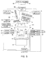
- Fig. 5 shows a second modification of the apparatus illustrated in Fig. 1.
- a half-transparent mirror or a half-silvered mirror 81 is arranged between the chopper 2 and the incident window 6a.
- a photo detector 83 is arranged in facing relation to the half-silvered mirror 81, and a narrow-band interference filter 82 is arranged between the half-silvered mirror 81 and the photo detector 83.
- the photo detector 83 is connected to a lock-in amplifier 84.
- the lock-in amplifier 84 and the lock-in amplifier 3 are connected to an arithmetic unit 85.
- the display 15 and the recorder 16 are connected to the arithmetic unit 85.
- a part of the light emitted from the light source 1 is reflected by the half-silvered mirror 81.
- the remaining light passes through the half-silvered mirror 81 and is incident upon the substrate 10 through the incident window 6a. That is, the light part is extracted from the light incident upon the substrate 10.
- the light part serves as a reference light.
- the light part reflected by the half-silvered mirror 81 is incident upon the photo detector 83 through the narrow-band interference filter 82.
- the lock-in amplifier 84 connected to the photo detector 83 issues an output on the basis of the light incident upon the photo detector 83.
- the reference light is compared with the reflected light incident upon the photo detector 4, in order to reduce instability in output from the light source 1.
- the epitaxial growing apparatus comprises a crystal growing device 130 which is one selected from a MO-CVD (metal organic-chemical vapor deposition) device, a chloride-method gas-phase growing device and a hydride epitaxial growing device. These devices are different from each other in gasses utilized. That is, AsCl 3 and H 2 are used in the chloride-method gas-phase growing device. HCl, H 2 , As 2 and As 4 are utilized in the hydride epitaxial growing device. Ga(CH 3 ) 3 , AsH 3 and H 2 are employed in the MO-CVD device.
- MO-CVD metal organic-chemical vapor deposition
- the crystal growing device 130 comprises a cylindrical quartz reaction tube 120 in which a closed chamber 141 is defined. Pressure within the closed chamber 141 is maintained at the normal pressure or atmospheric pressure to 1.33 Pa (10 -2 Torr), for example.
- the quartz reaction tube 120 has its one end provided with a gas introduction port 133, and the other end provided with a gas discharge port 134.
- Connected to the gas introduction port 133 is a supply nozzle 121 for gasses including GaAs crystal-growing raw material gasses and dopant.
- a plurality of control valves 123 are connected to the gas supply nozzle 121 and are also connected to a control system 112.
- a quartz susceptor 118 and a GaAs single-crystal substrate 117 are accommodated in the quartz reaction tube 120, that is, are placed within the closed chamber 141.
- a cylindrical heater 119 is arranged about the quartz reaction tube 120.
- An incident window 122a and an extraction window 122b, through which a light can pass, are arranged at their respective locations on both sides of the heater 119 and above the same.
- the incident window 122a and the extracting window 122b are arranged as follows.
- both the windows 122a and 122b are set in angle such that the light passing through the incident window 122a and the extracting window 122b is brought to a predetermined incident angle ⁇ 21 and a predetermined reflecting angle ⁇ 22 with respect to the GaAs single-crystal substrate 117.
- the arrangement is such that the light from a light source 101 is emitted to a growing film of the GaAs single-crystal substrate 117 from a predetermined direction.
- the light source 101 is arranged on the outside of the incident window 122a in facing relation thereto.
- the light source 101 is a source of a parallel beam, and is selected from a He-Ne laser, a semiconductor laser, a light-emitting diode, a mercury lamp and an argon ion laser.
- a chopper 102 for chopping the light from the light source 101 is arranged between the incident window 122a and the light source 101.
- a photo detector 104 for a light reflected from the substrate 117 is arranged on the outside of the extracting window 122b in facing relation thereto.
- a narrow-band interference filter 105 for removing a stray light from the reflected light is arranged between the extracting window 122b and the photo detector 104.
- the chopper 102 and the photo detector 104 are connected to a lock-in amplifier 103.
- the lock-in amplifier 103 is provided with a display 115 and a recorder 116.
- the lock-in amplifier 103 is connected to the control system 112.
- the crystal growing apparatus constructed as described above is used to carry out the epitaxial growing method for the chemical-compound crystal, according to the second embodiment of the invention, as follows.
- gas introduction time and evacuation time of the quartz reaction tube 120 are controlled by the control system 112.
- the raw-material gas containing Ga and the raw-material gas containing As are alternately supplied onto the GaAs single crystal substrate 117. In this manner, GaAs is epitaxially grown.
- the light from the light source 101 is reflected by the GaAs single-crystal substrate 117, and intensity of the reflected light is measured by the photo detector 104 such as a Si photodiode or the like.
- a detection output of the reflected-light intensity from the photo detector 104 is processed in signal by the lock-in amplifier 103. Subsequently, outputs are successively issued from the lock-in amplifier 103 to the display 115 and the recorder 116.
- the output from the lock-in amplifier 103 is inputted also to the control system 112. If a change in the reflected-light intensity corresponding to the desirable growing-film thickness per one cycle is reached, the control valve 123 is closed to stop introduction of the GaAs crystal growing raw-material gasses and the gas containing the dopant, thereby controlling the growing rate of the growing-film thickness. Thus, the desirable growing-film thickness is produced.
- the method according to the second embodiment of the invention can equally be applied to gas-phase growth using GaCl 3 and AsH 3 , chloride-method gas-phase growth due to Ga-AsCl 3 -H 2 , and hydride-method gas-phase growth using Ga-AsH 3 -HCl.
- the epitaxial growing apparatus comprises a molecular-beam epitaxial growing device 230 which is one of GaAs gas-phase growing devices.
- the molecular-beam epitaxial growing device 230 comprises a hermetic or closed container 241 in which a super-high vacuum growing chamber 226 is defined. Pressure within the super-high vacuum chamber 226 is maintained at 1.3 10 -2 to 1.3 10 -9 Pa (10 -4 to 10 -11 Torr), for example.
- a vacuum evacuation device 229 such as an ion pump, a turbo molecular pump or the like is connected to a bottom of the super-high vacuum growing chamber 226.
- a substrate heater 224 is arranged at a ceiling within the super-high vacuum growing chamber 226.
- a GaAs single-crystal substrate 225 is arranged adjacent the substrate heater 224 and facing downwardly.
- a plurality of raw-material heating crucibles 227 are fixedly supported on the bottom within the super-high vacuum growing chamber 226.
- a plurality of shutters 228 for controlling supply of molecular beams or raw-material gasses are provided respectively at openings of the respective raw-material heating crucibles 227.
- An incident window 229a and an extraction window 229b, through which a light can pass, are arranged respectively at opposed side walls of the super-high vacuum growing chamber 226.
- the incident window 229a and the extracting window 229b are arranged as follows.
- the incident window 229a and the extracting window 229b are set in angle such that the light passing through the incident window 229a and the extracting window 229b is brought to a predetermined incident angle ⁇ 31 and a predetermined reflecting angle ⁇ 32 with respect to the GaAs single-crystal substrate 225.
- the arrangement is such that a light from a light source 201 is emitted to a growing film of the GaAs single-crystal substrate 225 from a predetermined direction.
- the light source 201 is arranged on the outside of the incident window 229a in facing relation thereto.
- the light source 201 is a source of a parallel beam, and is selected from a He-Ne laser, a semiconductor laser, a light-emitting diode, a mercury lamp and an argon ion laser.
- a chopper 202 for chopping the light is arranged between the incident window 229a and the light source 201.
- a photo detector 204 for the light is arranged on the outside of the extracting window 229b in facing relation thereto.
- a narrow-band interference filter 205 for removing a stray light from the light reflected from the substrate 225 is arranged between the extracting window 229b and the photo detector 204.
- the chopper 202 and the photo detector 204 are connected to a lock-in amplifier 203.
- the lock-in amplifier 203 is provided with a display 215 and a recorder 216.
- the lock-in amplifier 203 is connected to a control system 212.
- control system 212 is connected to an electric system for the super-high vacuum growing chamber 226.
- the electric system is connected in line to attachment devices such as the shutters 228 and the like which are mounted within the super-high vacuum growing chamber 226.
- the epitaxial growing apparatus is used to carry out the epitaxial growing method for the chemical-compound crystal, according to the third embodiment of the invention, as follows.
- opening and closing operation of the shutters 228 is controlled by the control system 212.
- the raw materials within the respective crucibles 227 are heated respectively by the heaters 227, and the raw-material gasses are emitted from the crucibles 227 toward the substrate 225 when the shutters 228 are moved to their respective open positions.
- the raw-material gasses of respective Ga and As are alternately supplied onto the GaAs single-crystal substrate 225. In this manner, GaAs is epitaxially grown.
- the reflected-light intensity is measured as follows. That is, first, the light from the light source 201 arranged on the outside of the molecular-beam epitaxial growing device 230 is chopped by the chopper 202. Subsequently, the light is applied to the GaAs single-crystal substrate 225 through the incident window 229a. The light reflected from the substrate 225 is emitted toward the photo detector 204 through the extracting window 229b, and is measured by the photo detector 204 such as a Si photodiode or the like which is arranged on the outside of the molecular-beam epitaxial growing device 230. At the measurement due to the photo detector 204, a stray light is attenuated by the narrow-band interference filter 205 which is arranged between the photo detector 204 and the extracting window 229b.
- a detection output from the photo detector 204 is processed in signal by the lock-in amplifier 203. Subsequently, outputs are successively issued from the lock-in amplifier 203 to the display 215 and the recorder 216.
- the output from the lock-in amplifier 203 is also inputted to the control system 212.
- the desirable changing rate in the reflected-light intensity corresponding to the growing-film thickness per one cycle is stored in the control system 212. If a changing rate of the output from the lock-in amplifier 203 reaches a value of the stored desirable changing rate, the shutters 228 are closed.
- the growing rate of the growing-film thickness is controlled during growth of the crystal in the manner mentioned previously.
- the conventional RHEED is due to electron-beam diffraction, it is required that the direction of the crystal axis and the direction of the high-energy electron beam are aligned with each other. Thus, it is impossible for the conventional RHEED to grow the crystal while rotating the GaAs single-crystal substrate 10, 117 or 225.
- the change in the reflected-light intensity has no relation to the crystal axis, it is possible to grow the crystal while rotating the GaAs single-crystal substrate 10, 117 or 225. Thus, it is possible to secure uniformity in the plane of the crystal film.
Landscapes
- Chemical & Material Sciences (AREA)
- Chemical Kinetics & Catalysis (AREA)
- General Chemical & Material Sciences (AREA)
- Engineering & Computer Science (AREA)
- Materials Engineering (AREA)
- Metallurgy (AREA)
- Organic Chemistry (AREA)
- Crystallography & Structural Chemistry (AREA)
- Mechanical Engineering (AREA)
- Crystals, And After-Treatments Of Crystals (AREA)
Claims (18)
- Procédé de croissance épitaxiale d'un cristal de composé chimique afin de générer des couches monomoléculaires de façon alternée et indépendamment les unes des autres, comprenant :la mise en place d'un substrat de cristal (10) dans une enceinte fermée (31) d'un dispositif de croissance de cristaux (30) ;l'introduction alternée d'une pluralité de matières premières gazeuses dans ladite enceinte fermée (31) pour croítre ledit film de cristal monocouche par monocouche en utilisant lesdits gaz :pendant la croissance dudit cristal, émettre à partir d'une direction prédéterminée de la lumière vers un film de croissance de cristal dudit cristal ;mesurer l'intensité de la lumière réfléchie par ledit film de croissance de cristal ; etcontrôler les quantités de charge des matières premières gazeuses respectives sur la surface de croissance en fonction du changement d'intensité de la lumière réfléchie, ce qui permet de contrôler le taux de croissance du film de croissance et le nombre de couches monomoléculaires dudit cristal.
- Procédé selon la revendication 1, dans lequel ledit dispositif de croissance de cristal est un dispositif MO-CVD ou un dispositif de croissance épitaxiale à faisceau moléculaire.
- Procédé selon la revendication 1, comprenant en outre les étapes consistant à extraire une partie de la lumière émise vers ledit film de croissance de cristal, ladite partie de lumière servant de lumière de référence, et comparer ladite lumière de référence avec la lumière réfléchie afin de réduire l'instabilité en sortie d'une source de lumière.
- Procédé selon la revendication 1, dans lequel ladite lumière émise vers ledit film de croissance de cristal est un faisceau parallèle.
- Procédé selon la revendication 4, dans lequel ledit faisceau parallèle est émis à partir d'un laser à semi-conducteur, d'une diode à luminescence, d'une lampe à mercure, ou d'un laser à ion argon.
- Dispositif pour la croissance épitaxiale d'un cristal de composé chimique comprenantun dispositif de croissance de cristal (30) dans lequel est définie une enceinte fermée (31) et un dispositif d'évacuation à vide pour réduire la pression dans l'enceinte fermée (31) afin de croítre ledit cristal ;une lampe de chauffage (7) à l'extérieur de l'enceinte fermée (31), dirigée vers un film de croissance de cristal ;une pluralité de buses (8a, 8b) disposées en face dudit cristal pour introduire alternativement une pluralité de matières premières gazeuses dans l'enceinte fermée (31) afin de croítre ledit cristal ;une pluralité de buses (8a, 8b) disposées en face dudit cristal pour introduire des gaz d'impuretés dans ladite enceinte fermée (31), lesdites buses d'introduction de matières premières gazeuses et lesdites buses d'introduction de gaz d'impuretés (8a, 8b) étant disposées de façon opposée les unes par rapport aux autres ;des moyens de fenêtre incidente (6a) prévus à la périphérie de ladite enceinte fermée (31) ;des moyens de source de lumière (1) émettant une lumière de longueur d'onde prédéterminée qui est réfléchie par ledit cristal, lesdits moyens de source de lumière (1) étant disposés à l'extérieur de ladite enceinte fermée (31), en face desdits moyens de fenêtre incidente (6a), pour émettre de la lumière vers un film de croissance de cristal dudit cristal à travers lesdits moyens de fenêtre incidente (6a);des moyens de fenêtre d'extraction (6b) prévus à la périphérie de ladite enceinte fermée (31) ;des moyens (4) de réception de lumière présentant un angle prédéterminé pour recevoir la lumière réfléchie et rejeter la lumière incidente, lesdits moyens (4) de réception de lumière étant disposés à l'extérieur de ladite enceinte fermée (31), en face desdits moyens de fenêtre d'extraction (6b) ;des moyens (4) pour mesurer l'intensité de ladite lumière réfléchie ; etdes moyens de contrôle (12) pour contrôler les quantités de charge des matières premières gazeuses respectives en fonction du changement de l'intensité de la lumière réfléchie, contrôlant ainsi le taux de croissance et le nombre de couchesmonomoléculaires dudit cristal.
- Dispositif selon la revendication 6, dans lequel ledit moyen de source de lumière est une source d'un faisceau parallèle.
- Dispositif selon la revendication 7, dans lequel ladite source du faisceau parallèle est un laser à semi-conducteur, une diode à luminescence, une lampe à mercure ou un laser à ion argon.
- Dispositif selon la revendication 6, dans lequel ledit dispositif de croissance de cristal est un dispositif MO-CVD ou un dispositif de croissance épitaxiale à faisceau moléculaire.
- Dispositif selon la revendication 6, comprenant en outre des moyens de filtre disposés entre lesdits moyens de fenêtre d'extraction et lesdits moyens de réception de lumière, pour rejeter la lumière parasite provenant de ladite lumière réfléchie.
- Dispositif selon la revendication 10, dans lequel lesdits moyens de filtre sont constitués par un filtre à bande d'interférence.
- Dispositif selon la revendication 10, dans lequel lesdits moyens de filtre sont constitués par un filtre à bande d'interférence étroite.
- Dispositif selon la revendication 6, comprenant en outre des moyens d'extraction pour extraire une partie de la lumière émise vers ledit film de croissance de cristal, ladite partie de lumière servant de lumière de référence, et des moyens pour comparer ladite lumière de référence avec la lumière réfléchie afin de réduire l'instabilité en sortie d'une source de lumière.
- Dispositif suivant la revendication 6, dans lequel ledit dispositif de croissance de cristal est un dispositif de croissance épitaxiale pourvu d'un réservoir fermé, ladite enceinte fermée étant définie dans ledit réservoir fermé.
- Dispositif selon la revendication 6, dans lequel ledit dispositif de croissance de cristal comporte un tube de réaction à quartz cylindrique, ladite enceinte fermée étant définie dans ledit tube de réaction à quartz cylindrique, et dans lequel ledit tube de réaction à quartz cylindrique est pourvu, à l'une de ses extrémités, d'un embout d'introduction de gaz à travers lequel lesdites matières premières gazeuses sont introduites dans ladite enceinte fermée, et ledit tube de réaction à quartz cylindrique est pourvu, à son autre extrémité, d'un embout de sortie de gaz, à travers lequel lesdites matières premières gazeuses sont évacuées de ladite enceinte fermée.
- Dispositif selon la revendication 6, dans lequel ledit dispositif de croissance de cristal est un dispositif de croissance épitaxiale à faisceau moléculaire pourvu d'un réservoir fermé dans lequel une chambre à vide extrême est définie, ladite chambre à vide extrême servant d'enceinte fermée.
- Dispositif selon la revendication 6, dans lequel ledit cristal de composé chimique est monté de façon fixe à la périphérie de ladite enceinte fermée.
- Dispositif selon la revendication 6, dans lequel ledit cristal de composé chimique est monté à la périphérie de ladite enceinte fermée de façon à tourner autour d'un axe.
Applications Claiming Priority (2)
| Application Number | Priority Date | Filing Date | Title |
|---|---|---|---|
| JP1305873A JPH0751478B2 (ja) | 1989-11-24 | 1989-11-24 | 化合物結晶のエピタキシャル成長方法 |
| JP305873/89 | 1989-11-24 |
Publications (3)
| Publication Number | Publication Date |
|---|---|
| EP0431415A2 EP0431415A2 (fr) | 1991-06-12 |
| EP0431415A3 EP0431415A3 (en) | 1993-10-06 |
| EP0431415B1 true EP0431415B1 (fr) | 1998-01-21 |
Family
ID=17950373
Family Applications (1)
| Application Number | Title | Priority Date | Filing Date |
|---|---|---|---|
| EP90122371A Expired - Lifetime EP0431415B1 (fr) | 1989-11-24 | 1990-11-23 | Procédé et appareillage pour la croissance épitaxiale d'un cristal d'un composé chimique |
Country Status (4)
| Country | Link |
|---|---|
| US (1) | US5463977A (fr) |
| EP (1) | EP0431415B1 (fr) |
| JP (1) | JPH0751478B2 (fr) |
| DE (1) | DE69031976T2 (fr) |
Families Citing this family (16)
| Publication number | Priority date | Publication date | Assignee | Title |
|---|---|---|---|---|
| JP2987379B2 (ja) * | 1991-11-30 | 1999-12-06 | 科学技術振興事業団 | 半導体結晶のエピタキシャル成長方法 |
| US5582646A (en) * | 1994-10-21 | 1996-12-10 | J.A. Woollam Co. Inc. | Ellipsometer/polarimeter based process monitor and control system suitable for simultaneous retrofit on molecular beam epitaxy system RHEED/LEED interface system, and method of use |
| US5552327A (en) * | 1994-08-26 | 1996-09-03 | North Carolina State University | Methods for monitoring and controlling deposition and etching using p-polarized reflectance spectroscopy |
| US6409828B1 (en) * | 1994-10-31 | 2002-06-25 | Texas Instruments Incorporated | Method and apparatus for achieving a desired thickness profile in a flow-flange reactor |
| JPH08139416A (ja) * | 1994-11-14 | 1996-05-31 | Sony Corp | 化合物半導体層の臨界膜厚の求め方およびそれを用いた光半導体装置の製造方法 |
| KR970053234A (ko) * | 1995-12-20 | 1997-07-31 | 양승택 | 화합물 반도체의 도핑특성을 실시간으로 감지하는 방법 |
| US5872016A (en) * | 1996-06-18 | 1999-02-16 | Lucent Technologies Inc. | Process of making an optoelectronic devices utilizing multiple quantum well pin structures |
| KR100368318B1 (ko) * | 2000-12-29 | 2003-01-24 | 주식회사 하이닉스반도체 | 반도체 소자의 선택적 에피택셜 성장법 |
| US6994750B2 (en) * | 2001-09-10 | 2006-02-07 | Matsushita Electric Industrial Co., Ltd. | Film evaluating method, temperature measuring method, and semiconductor device manufacturing method |
| US7342225B2 (en) * | 2002-02-22 | 2008-03-11 | Agere Systems, Inc. | Crystallographic metrology and process control |
| KR100979071B1 (ko) * | 2002-02-22 | 2010-08-31 | 에이저 시스템즈 인크 | 이중 배향 다결정성 재료의 화학 기계적 연마 |
| JP2006128559A (ja) * | 2004-11-01 | 2006-05-18 | Tokyo Electron Ltd | 基板処理システム |
| GB0516477D0 (en) | 2005-08-11 | 2005-09-14 | Optical Reference Systems Ltd | Apparatus for measuring semiconductor physical characteristics |
| US20130000545A1 (en) * | 2011-06-28 | 2013-01-03 | Nitride Solutions Inc. | Device and method for producing bulk single crystals |
| TWI684680B (zh) | 2013-09-04 | 2020-02-11 | 奈瑞德解決方案公司 | 體擴散長晶法 |
| JP6172672B2 (ja) * | 2013-10-11 | 2017-08-02 | 大陽日酸株式会社 | 気相成長装置の膜厚測定方法 |
Family Cites Families (20)
| Publication number | Priority date | Publication date | Assignee | Title |
|---|---|---|---|---|
| US3915765A (en) * | 1973-06-25 | 1975-10-28 | Bell Telephone Labor Inc | MBE technique for fabricating semiconductor devices having low series resistance |
| JPS5033772A (fr) * | 1973-07-25 | 1975-04-01 | ||
| JPS5032878A (fr) * | 1973-07-25 | 1975-03-29 | ||
| JPS52124859A (en) * | 1976-04-14 | 1977-10-20 | Hitachi Ltd | Continuous vapor phase growth apparatus |
| US4159919A (en) * | 1978-01-16 | 1979-07-03 | Bell Telephone Laboratories, Incorporated | Molecular beam epitaxy using premixing |
| EP0031180A3 (fr) * | 1979-12-19 | 1983-07-20 | Philips Electronics Uk Limited | Procédé de croissance d'une couche d'un composé III-V dopé par épitaxie par faisceau moléculaire et dispositif semiconducteur comportant un substrat semiconducteur muni d'une couche épitaxiale d'un composé III-V dopé déposé par ce procédé |
| US4525376A (en) * | 1982-03-16 | 1985-06-25 | Energy Conversion Devices, Inc. | Optical methods for controlling layer thickness |
| FR2531774A1 (fr) * | 1982-08-12 | 1984-02-17 | Cit Alcatel | Dispositif de controle d'epaisseur de couches minces faiblement absorbantes |
| GB2130716A (en) * | 1982-11-26 | 1984-06-06 | Philips Electronic Associated | Method of determining the composition of an alloy film grown by a layer-by layer process |
| JPS59192904A (ja) * | 1983-04-15 | 1984-11-01 | Hitachi Ltd | 膜厚測定装置 |
| JPS6283878U (fr) * | 1985-11-18 | 1987-05-28 | ||
| JPS62173711A (ja) * | 1986-01-28 | 1987-07-30 | Canon Inc | 光反応プロセスのモニタ−方法 |
| CA1302803C (fr) * | 1986-02-15 | 1992-06-09 | Hiroji Kawai | Appareil de metallisation par depot sous vide et methode connexe |
| GB8606748D0 (en) * | 1986-03-19 | 1986-04-23 | Secr Defence | Monitoring surface layer growth |
| JPH0730448B2 (ja) * | 1986-08-01 | 1995-04-05 | 松下電器産業株式会社 | 薄膜形成方法 |
| US4812650A (en) * | 1987-09-08 | 1989-03-14 | Varian Associates, Inc. | Growth rate monitor for molecular beam epitaxy |
| WO1989006354A1 (fr) * | 1988-01-11 | 1989-07-13 | The Commonwealth Of Australia | Ellipsometre differentiel |
| JPH0274588A (ja) * | 1988-09-12 | 1990-03-14 | Nec Corp | 気相成長装置 |
| US4931132A (en) * | 1988-10-07 | 1990-06-05 | Bell Communications Research, Inc. | Optical control of deposition of crystal monolayers |
| US5091320A (en) * | 1990-06-15 | 1992-02-25 | Bell Communications Research, Inc. | Ellipsometric control of material growth |
-
1989
- 1989-11-24 JP JP1305873A patent/JPH0751478B2/ja not_active Expired - Fee Related
-
1990
- 1990-11-23 DE DE69031976T patent/DE69031976T2/de not_active Expired - Fee Related
- 1990-11-23 EP EP90122371A patent/EP0431415B1/fr not_active Expired - Lifetime
-
1993
- 1993-07-15 US US08/091,747 patent/US5463977A/en not_active Expired - Lifetime
Also Published As
| Publication number | Publication date |
|---|---|
| JPH0751478B2 (ja) | 1995-06-05 |
| DE69031976D1 (de) | 1998-02-26 |
| EP0431415A3 (en) | 1993-10-06 |
| EP0431415A2 (fr) | 1991-06-12 |
| DE69031976T2 (de) | 1998-08-20 |
| JPH03164497A (ja) | 1991-07-16 |
| US5463977A (en) | 1995-11-07 |
Similar Documents
| Publication | Publication Date | Title |
|---|---|---|
| EP0545238B1 (fr) | Procédé de croissance d'un cristal semi-conducteur | |
| EP0431415B1 (fr) | Procédé et appareillage pour la croissance épitaxiale d'un cristal d'un composé chimique | |
| US5525156A (en) | Apparatus for epitaxially growing a chemical compound crystal | |
| US4975252A (en) | Semiconductor crystal growth apparatus | |
| US4806321A (en) | Use of infrared radiation and an ellipsoidal reflection mirror | |
| US4945254A (en) | Method and apparatus for monitoring surface layer growth | |
| US5399521A (en) | Method of semiconductor layer growth by MBE | |
| JP2001516022A (ja) | 薄膜の原位置厚み及び化学量論測定のための装置及び方法 | |
| Irvine et al. | A study of the growth kinetics of II–VI metalorganic vapour phase epitaxy using in situ laser reflectometry | |
| JPH07153692A (ja) | 半導体基板上に薄膜を成長させる方法および装置 | |
| Irvine et al. | Complete in situ laser monitoring of MOCVD HgCdTe/CdTe/ZnTe growth onto GaAs substrates | |
| EP0132408A2 (fr) | Procédé et appareil pour faire croître des couches ou pour produire des revêtements sur un substrat | |
| US5364492A (en) | Method of deposing by molecular beam epitaxy | |
| JPS5948786B2 (ja) | 分子線結晶成長方法 | |
| Roth | Closed-loop control of MBE using an integrated multi-sensor system | |
| ASPNES | REAL-TIME SURFACE AND NEAR-SURFACE OPTICAL DIAGNOSTICS | |
| JPS6350394A (ja) | 分子線結晶成長装置 | |
| Kasai et al. | MBE growth of BiSrCaCuO films using flux monitoring by atomic absorption spectroscopy | |
| Almeida et al. | In Situ Spectroscopic Ellipsometry for Monitoring and Control of HgCdTe Heterostructures Grown by Molecular Beam Epitaxy | |
| Buoncristiani et al. | Spectroscopic analysis of insulating crystal fibers | |
| Sukidi et al. | GaxIn1-xP/GaP Heterostructures on Si (001) Substrate | |
| JPS6278186A (ja) | 粒子線エピタキシヤル装置 | |
| JPS61219791A (ja) | 粒子線エピタキシヤル装置の粒子線強度検出制御装置 | |
| ALMEIDA et al. | IZV 5771/SPECTROSCOPIC ELLIPSOMETRY FOR MONITORING AND CONTROL OF HgCdTe HETEROSTRUCTURES GROWN BY MOLECULAR BEAM EPITAXY | |
| JPH01176292A (ja) | 分子線エピタキシャル成長方法及び装置 |
Legal Events
| Date | Code | Title | Description |
|---|---|---|---|
| PUAI | Public reference made under article 153(3) epc to a published international application that has entered the european phase |
Free format text: ORIGINAL CODE: 0009012 |
|
| AK | Designated contracting states |
Kind code of ref document: A2 Designated state(s): DE GB |
|
| PUAL | Search report despatched |
Free format text: ORIGINAL CODE: 0009013 |
|
| AK | Designated contracting states |
Kind code of ref document: A3 Designated state(s): DE GB |
|
| 17P | Request for examination filed |
Effective date: 19940331 |
|
| 17Q | First examination report despatched |
Effective date: 19950515 |
|
| GRAG | Despatch of communication of intention to grant |
Free format text: ORIGINAL CODE: EPIDOS AGRA |
|
| GRAH | Despatch of communication of intention to grant a patent |
Free format text: ORIGINAL CODE: EPIDOS IGRA |
|
| GRAH | Despatch of communication of intention to grant a patent |
Free format text: ORIGINAL CODE: EPIDOS IGRA |
|
| GRAA | (expected) grant |
Free format text: ORIGINAL CODE: 0009210 |
|
| AK | Designated contracting states |
Kind code of ref document: B1 Designated state(s): DE GB |
|
| REF | Corresponds to: |
Ref document number: 69031976 Country of ref document: DE Date of ref document: 19980226 |
|
| PLBE | No opposition filed within time limit |
Free format text: ORIGINAL CODE: 0009261 |
|
| STAA | Information on the status of an ep patent application or granted ep patent |
Free format text: STATUS: NO OPPOSITION FILED WITHIN TIME LIMIT |
|
| 26N | No opposition filed | ||
| REG | Reference to a national code |
Ref country code: GB Ref legal event code: IF02 |
|
| PGFP | Annual fee paid to national office [announced via postgrant information from national office to epo] |
Ref country code: GB Payment date: 20061127 Year of fee payment: 17 |
|
| PGFP | Annual fee paid to national office [announced via postgrant information from national office to epo] |
Ref country code: DE Payment date: 20070116 Year of fee payment: 17 |
|
| GBPC | Gb: european patent ceased through non-payment of renewal fee |
Effective date: 20071123 |
|
| PG25 | Lapsed in a contracting state [announced via postgrant information from national office to epo] |
Ref country code: DE Free format text: LAPSE BECAUSE OF NON-PAYMENT OF DUE FEES Effective date: 20080603 |
|
| PG25 | Lapsed in a contracting state [announced via postgrant information from national office to epo] |
Ref country code: GB Free format text: LAPSE BECAUSE OF NON-PAYMENT OF DUE FEES Effective date: 20071123 |