EP0431492B1 - Leistungswandler vom Brückentyp mit verbessertem Wirkungsgrad - Google Patents
Leistungswandler vom Brückentyp mit verbessertem Wirkungsgrad Download PDFInfo
- Publication number
- EP0431492B1 EP0431492B1 EP90122961A EP90122961A EP0431492B1 EP 0431492 B1 EP0431492 B1 EP 0431492B1 EP 90122961 A EP90122961 A EP 90122961A EP 90122961 A EP90122961 A EP 90122961A EP 0431492 B1 EP0431492 B1 EP 0431492B1
- Authority
- EP
- European Patent Office
- Prior art keywords
- switching element
- signal
- terminal
- switching elements
- terminals
- Prior art date
- Legal status (The legal status is an assumption and is not a legal conclusion. Google has not performed a legal analysis and makes no representation as to the accuracy of the status listed.)
- Expired - Lifetime
Links
Images


Classifications
-
- H—ELECTRICITY
- H02—GENERATION; CONVERSION OR DISTRIBUTION OF ELECTRIC POWER
- H02M—APPARATUS FOR CONVERSION BETWEEN AC AND AC, BETWEEN AC AND DC, OR BETWEEN DC AND DC, AND FOR USE WITH MAINS OR SIMILAR POWER SUPPLY SYSTEMS; CONVERSION OF DC OR AC INPUT POWER INTO SURGE OUTPUT POWER; CONTROL OR REGULATION THEREOF
- H02M7/00—Conversion of AC power input into DC power output; Conversion of DC power input into AC power output
- H02M7/42—Conversion of DC power input into AC power output without possibility of reversal
- H02M7/44—Conversion of DC power input into AC power output without possibility of reversal by static converters
- H02M7/48—Conversion of DC power input into AC power output without possibility of reversal by static converters using discharge tubes with control electrode or semiconductor devices with control electrode
- H02M7/53—Conversion of DC power input into AC power output without possibility of reversal by static converters using discharge tubes with control electrode or semiconductor devices with control electrode using devices of a triode or transistor type requiring continuous application of a control signal
- H02M7/537—Conversion of DC power input into AC power output without possibility of reversal by static converters using discharge tubes with control electrode or semiconductor devices with control electrode using devices of a triode or transistor type requiring continuous application of a control signal using semiconductor devices only, e.g. single switched pulse inverters
- H02M7/5387—Conversion of DC power input into AC power output without possibility of reversal by static converters using discharge tubes with control electrode or semiconductor devices with control electrode using devices of a triode or transistor type requiring continuous application of a control signal using semiconductor devices only, e.g. single switched pulse inverters in a bridge configuration
-
- H—ELECTRICITY
- H02—GENERATION; CONVERSION OR DISTRIBUTION OF ELECTRIC POWER
- H02M—APPARATUS FOR CONVERSION BETWEEN AC AND AC, BETWEEN AC AND DC, OR BETWEEN DC AND DC, AND FOR USE WITH MAINS OR SIMILAR POWER SUPPLY SYSTEMS; CONVERSION OF DC OR AC INPUT POWER INTO SURGE OUTPUT POWER; CONTROL OR REGULATION THEREOF
- H02M3/00—Conversion of DC power input into DC power output
-
- H—ELECTRICITY
- H10—SEMICONDUCTOR DEVICES; ELECTRIC SOLID-STATE DEVICES NOT OTHERWISE PROVIDED FOR
- H10W—GENERIC PACKAGES, INTERCONNECTIONS, CONNECTORS OR OTHER CONSTRUCTIONAL DETAILS OF DEVICES COVERED BY CLASS H10
- H10W90/00—Package configurations
- H10W90/701—Package configurations characterised by the relative positions of pads or connectors relative to package parts
- H10W90/751—Package configurations characterised by the relative positions of pads or connectors relative to package parts of bond wires
- H10W90/754—Package configurations characterised by the relative positions of pads or connectors relative to package parts of bond wires between a chip and a stacked insulating package substrate, interposer or RDL
Definitions
- the present invention relates to a bridge type power converter using a self turn-off element and having improved driving and protecting characteristics.
- IGBT Insulated Gate Bipolar Transistor
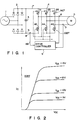
- Fig. 2 shows V CE (collector-emitter voltage) vs. I C (collector current) characteristics using a drive voltage V GE (gate-emitter voltage) of the IGBT as a parameter.
- V CE collector-emitter voltage
- I C collector current
- V GE gate-emitter voltage
- the transistor type power element however, has comparatively high voltage V CE with respect to a given constant current I C , i.e., has a high DC resistance.
- a switching element of this inverter bridge can be constituted by an MCT (MOS Controlled Thyristor).
- MCT MOS Controlled Thyristor
- a reactor for suppressing a current increase rate is connected between a DC power source and the inverter bridge, and a high-speed diode for suppressing a surge voltage generated by the reactor is connected therebetween in parallel with the reactor.
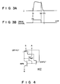
- the MCT has a thyristor structure constituted by PNP and NPN transistors as shown in Fig. 4.
- a thyristor structure constituted by PNP and NPN transistors as shown in Fig. 4.
- the NPN transistor When an ON FET is turned on by a gate signal, the NPN transistor is turned on, and the PNP transistor is turned on. Therefore, the MCT is self-held to perform an operation equivalent to that of a thyristor and exhibits a low voltage drop characteristic between the anode and cathode.
- an OFF FET is turned on by the gate signal, the base-emitter path of the PNP transistor is short-circuited to turn off the PNP transistor, and the NPN transistor is turned off, thereby stopping the thyristor operation.
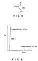
- Fig. 5 shows a circuit symbol of the MCT.
- Fig. 6 shows anode current I A vs. anode-cathode voltage V A-K characteristics of the MCT. As shown in Fig. 7, almost no current flows when the MCT is OFF, and a voltage drop exhibits a low value when the MCT is turned on. In addition, unlike a transistor type element, the MCT has no constant-current characteristic and therefore can be considered as a low resistance resistor when it is turned on.
- a protection operation is performed as shown in Figs. 3A and 3B. That is, after the transistor is turned on at time t1 (Fig. 3B), an overcurrent is detected at a time t2 (Fig. 3A) to turn off a drive signal, thereby safely shutting off a failure current suppressed by a constant-current characteristic of the transistor till time t3 (Fig. 3A).
- the transistor type element Since, however, the transistor type element has a large voltage drop in V CE for a large I C (i.e., a DC resistance is high) as shown in Fig. 2, a power loss in an inverter portion is large to result in a low efficiency.
- the MCT has a high efficiency because a voltage drop is small when it is turned on, it requires a reactor and a high-speed diode for suppressing a surge voltage.
- the reactor since the reactor must have a large capacity so as not to be saturated even with an overcurrent, an inverter having a small or middle capacity cannot be economically designed.
- a main circuit and a driver of a voltage type inverter generally use as an inverter bridge element an IGBT and a self-extinguishing element such as a MOSFET, a bipolar transistor, and an MCT.
- the circuit is arranged such that a DC power output is supplied to a transistor bridge via a high-speed fuse, the DC power is converted into AC power by a switching operation of the bridge, and the converted power is supplied to a load.
- the above transistor bridge constitutes a 3-phase bridge by IGBTs.
- Each IGBT on the positive side is driven by supplying a drive signal from an individual drive power source to the gate of the IGBT.
- a gate drive signal can be supplied from a common drive power source to the gates of the IGBTs.
- transistors are elements called a module type in which a main electrode and a cooling surface are electrically insulated and a transistor chip in the module is connected to an electrode outside the module through a bonding wire.
- a transistor connected to the positive and negative sides is broken (deteriorated) to short-circuit the positive and negative terminals of a DC power source, an overcurrent flows through the transistor to fuse the bonding wire in the module.
- an arc is generated to dangerously scatter the outer wall of the module type transistor. Therefore, a high-speed fuse is used to interrupt a failure current.
- a high-speed fuse is connected to the collector of each IGBT because it is practically difficult to obtain a common fuse suited to protect the individual module elements connected in parallel with each other.
- the fuse is connected to the collector of each IGBT because a gate drive signal of the IGBT must be commonly applied to the emitter and the gate of the IGBT.
- a rate (di/dt) of change in a switching current is increased to a value several times that of a conventional bipolar transistor, and a surge voltage is increased accordingly. Therefore, a conventional circuit arrangement cannot be practically adopted.
- a surge energy between the connector and the emitter of an IGBT may be clamped by a series circuit of a capacitor and a diode, and the clamped energy is then discharged via a resistor.
- Prior art document EP-A-50 753 discloses a bridge type power converter having features similar to those included in the precharacterizing part of claim 1, wherein first and third switching elements being represented by GTO thyristors and second and further switching elements being represented by transistors.
- the present invention provides a bridge type power converter as specified in anyone of claims 1, 7 and 8.
- one of series-connected semiconductor elements in the inverter bridge is constituted by a first self-extinguishing switching element such as an MCT having a low-loss characteristic (substantially constant-voltage characteristic) with a small voltage drop under conduction
- the other semiconductor element is constituted by a second self-extinguishing switching element such as an IGBT having a constant-current characteristic with a current suppressed in accordance with a drive signal.
- a failure current is suppressed by a current-suppressing effect of the second self-extinguishing switching element and safely interrupted by turning off the first and second self-extinguishing switching elements.
- the emitter of the IGBT which is turned on/off by a drive signal supplied between the emitter and the gate, and the anode of the MCT which is turned on/off by a drive signal supplied between the anode and the gate are connected to be used as an output terminal;
- the collector of the IGBT is connected to the positive side of a DC bus via a fuse;
- the cathode of the MCT is connected to the negative side of the DC bus via a fuse;
- a snubber circuit is connected between the collector of the IGBT and the cathode of the MCT.
- a common drive power source is used for the IGBTs, and a common drive power source is used for the MCTs.
- a snubber capacitor is connected between the collector and the cathode to absorb a surge energy caused by an inductance of the fuse circuit, thereby preventing the surge voltage from being applied to the elements (IGBT and MCT).
- the IGBTs and the anodes of the MCTs are commonly connected, the IGBTs and the MCTs can be driven by common drive power sources, respectively.
- An AC voltage from AC power source 1 is converted into a DC voltage by diode bridge 2 and smoothed by capacitor 3. This DC voltage is converted into a second AC voltage by inverter bridge 4 and supplied to load motor 5.
- MCTs 51, 53, and 55 are connected to positive DC bus P of inverter bridge 4, and IGBTs 42, 44, and 46 are connected to its negative DC bus N.
- a load current is detected by current detectors 6 and 7, and a DC current is detected by current detector 8.
- drive controller 9 detects output levels from these current detectors and turns off a drive signal, thereby shutting off the overcurrent to perform a protection operation.
- a current flows from the DC power source (1 to 3) to load 5 through the MCTs and the IGBTs.
- a failure current is suppressed by a transistor effect (constant-current characteristic) of the IGBT.
- the MCTs and the IGBTs are rapidly turned off by controller 9, the current can be interrupted below a maximum interrupting current of the MCT.
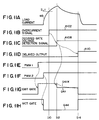
- Fig. 8 is a block diagram showing a configuration of the drive controller in Fig. 1.
- Figs. 9A to 9F are waveforms illustrating an operation of the drive controller in Fig. 8.
- DC current signal e8 exceeds predetermined overcurrent detection level IL1 shown in Fig. 9A
- overcurrent detector 102 generates overcurrent signal e102 at time t10 as shown in Fig. 9B.
- Overcurent signal e102 is supplied to AND gates 104 and 105.
- PWM controller 103 supplies pulse-width modulation control signals PWM1 and PWM2, as shown in Figs. 9C and 9D, to AND gates 104 and 105, respectively.
- Gate 104 supplies logical product e104 of signals e102 and PWM1 to gate circuit 106
- gate 105 supplies logical product e105 of signals e102 and PWM2 to gate circuit 107.
- circuit 106 supplies IGBT gate signal G41, as shown in Fig. 9E, to each of IGBT's 42-46, and circuit 107 supplies MCT gate signal G44, as shown in Fig. 9F, to each of MCT's 51-55.
- gate signals G41 and G44 becomes OFF signals at time t10 at which an overcurrent is detected, and slightly after time t10, both the IGBT and MCT in each arm of the inverter shown in Fig. 1 are turned OFF.
- Fig. 10 is a block diagram showing a configuration of the drive controller in Fig. 1.
- Figs. 11A to 11F are waveforms illustrating an operation of the drive controller in Fig. 10.
- a load current is detected as load current signal e8 by current transformer 8.
- load current signal e8 exceeds predetermined overcurrent detection level IL1 shown in Fig. 11A
- overcurrent detector 102 generates overcurrent signal e102 at time t10 as shown in Fig. 11B.
- Overcurrent signal e102 is supplied to decayed gate voltage generator 108 and delay circuit 110.
- generator 108 After elapsing a predetermined period of time (e.g., 0.3 to 0.5 ⁇ sec.) from time t10, generator 108 generates step signal e108 having a predetermined signal level as shown at time t12 in Fig. 11C. Meanwhile, after elapsing another predetermined period of time (e.g., 5 to 10 ⁇ sec.) from time t10, circuit 110 generates delayed signal e110 as shown at time t14 in Fig. 11D.
- a predetermined period of time e.g., 0.3 to 0.5 ⁇ sec.
- generator 108 After elapsing another predetermined period of time (e.g., 5 to 10 ⁇ sec.) from time t10, circuit 110 generates delayed signal e110 as shown at time t14 in Fig. 11D.
- PWM controller 103 generates pulse-width modulation control signals PWM1 and PWM2, as shown in Figs. 11E and 11F, respectively.
- Signals PWM1 and PWM2 are supplied to AND gates 104 and 105, respectively. Both gates 104 and 105 receives delayed signal e110 from delay circuit 110.
- Gate 104 supplies logical product e104 of signals PWM1 and e110 to gate circuit 106, and gate 105 supplies logical product e105 of signals e110 and PWM2 to gate circuit 107.
- Gate circuit 106 receives step signal e108 from decayed gate voltage generator 108, and modulates the amplitude of IGBT gate signal G41 by signal e108. Then, circuit 106 supplies IGBT gate signal G41, having a waveform as shown in Fig. 11G, to each of IGBT's 42-46, and circuit 107 supplies MCT gate signal G44, as shown in Fig. 11H, to each of MCT's 51-55. (The amplitude of the IGBT gate signal may be decayed exponentially, as is shown by broken line G41* in Fig. 11G).
- the overcurrent, flowing through the collector-emitter path of the IGBT can be detected by detecting the value of collector-emitter voltage V CE of each IGBT.
- Such an overcurrent detection using V CE can be used in place of overcurrent detector 102 in Fig. 8 or 10.
- the low-loss characteristic (constant-voltage characteristic) of the MCT and the constant-current characteristic of the IGBT can be effectively used to improve an operation efficiency and interrupt an overcurrent caused by a load short-circuit or the like within a safe interrupting current of an MCT without using large equipment such as a reactor. Therefore, a compact and economical bridge type power converter can be obtained.
- the MCTs are arranged at the positive side of the DC bus, only one gate power source need be used for the MCTs.
- the IGBTs are arranged at the negative side of the DC bus, only one gate power source need be used for the IGBTs. Therefore, a very compact and economical bridge type power converter can be obtained.
- the number of series-connected elements or the arrangement of a bridge is not limited to such an inverter bridge.
- the present invention can be applied to the configurations as shown in Figs. 16 to 18.
- the element is not limited to the MCT and the IGBT.
- a Field Electric Transistor (FET), Static Induced Transistor (SIT), Static Induced Thyristor (SITH), Gate Turn-Off Thyristor (GTO), and the like can be used for the above elements.
- a switching element having a low-loss characteristic such as a thyristor
- a high-efficiency operation can be performed.
- a switching element having a constant-current characteristic such as a transistor (IGBT)
- IGBT transistor
- MCTs are connected as switching elements having a low-loss characteristic to the positive side of a DC bus
- IGBTs are connected as switching elements having a constant-current characteristic to the negative side of the DC bus. Therefore, the size of a gate drive power source can be minimized to realize a compact and economical bridge type power converter.
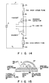
- Fig. 12 shows one phase of an inverter bridge.
- Positive side P of a DC bus of power supply 10 is connected to the collectors of IGBTs 41a, 41b, and 41c via fuses 31a, 31b, and 31c, respectively.
- the emitters of IGBTs 41a, 41b, and 41c are connected in parallel with each other and connected to parallel-connected anodes of MCTs 54a, 54b, and 54c to form output terminal G0 of the bridge.
- the cathodes of MCTs 54a, 54b, and 54c are connected to negative side N of the DC bus, via fuses 32a, 32b, and 32c, respectively.
- the gates of IGBTs 41a, 41b, and 41c are connected in parallel to terminal G41, and the gates of MCTs 54a, 54b, and 54c are connected in parallel to terminal G44.
- Snubber capacitor 6a is connected between the collector of IGBT 41a and the cathode of MCT 54a.
- Snubber capacitor 6b is connected between the collector of IGBT 41b and the cathode of MCT 54b.
- Snubber capacitor 6c is connected between the collector of IGBT 41c and the cathode of MCT 54c.
- a gate drive signal is supplied to gate G41 of the IGBTs, via intermediate point G0 between driver power sources 11a and 11b and IGBT driver 106, and is supplied to gate G44 of the MCTs, via intermediate point G0 and MCT driver 107.
- Common point G0 of a gate signal is common to the IGBTs and the MCTs.
- Fig. 15 shows a practical structure of a module transistor.
- thermally-conductive ceramic plate 81 is adhered on copper base 80 for causing a cooling fin to radiate heat, and copper electrode 82, collector electrode 83, and emitter electrode 84 are adhered on ceramic plate 81.
- Pellet 85 of the transistor has a collector adhered on copper electrode 82 and an emitter terminal adhered thereon which is connected to emitter electrode 84 through bonding wire 87.
- Bonding wire 86 is connected to collector electrode 83 and extracted as a collector.
- a failure current must be interrupted by a high-speed fuse before this fusing.
- the gate drive power source can be commonly used for both the upper and lower elements of the bridge, a compact and economical bridge can be provided.
- Fig. 20 shows a circuit of one phase of an inverter constituted by a P/N complementary IGBTs.
- Gate signals supplied to P/N IGBTs in Fig. 20 may have waveforms as shown in Fig. 21A and 21B.
- periods Tx1 and Tx2 is provided to prevent simultaneous turning on of the two P/N IGBTs.
- the snubber circuit can adopt various types of combinations of, e.g., diodes, capacitors, and resistors, as shown in Figs. 22A to 22C.
- a single fuse may be inserted for a plurality of elements, as shown in Fig. 19.
- a fuse is connected in series with an element to prevent a rupture of the outer wall of the element.
- a switching energy caused by an increase in inductance produced by connecting the fuse is absorbed by the snubber circuit provided to an element side DC terminal of the bridge, thereby giving a margin to a safe operation region of the switching element. Therefore, reliability of the bridge can be improved, and its efficiency can be increased because a switching loss is reduced.
- a common drive power source can be used for both the upper and lower elements of the bridge, a compact and economical semiconductor switching element bridge circuit can be provided.
Landscapes
- Engineering & Computer Science (AREA)
- Power Engineering (AREA)
- Inverter Devices (AREA)
- Dc-Dc Converters (AREA)
Claims (9)
- Brückentyp-Leistungswandler mit:einem ersten Schaltelement (51), das mit ersten und zweiten Anschlüssen versehen ist und einen niedrigen leitenden Widerstandswert, jedoch keine Strombegrenzungskennlinie hat (Fig. 6),einem zweiten Schaltelement (42), das mit ersten und zweiten Anschlüssen versehen ist und im wesentlichen eine konstante Stromkennlinie hat (Fig. 2),einem dritten Schaltelement (53), das mit ersten und zweiten Anschlüssen versehen ist und einen niedrigen leitenden Widerstandswert, jedoch keine Strombegrenzungskennlinie hat (Fig. 6),einem vierten Schaltelement (44), das mit ersten und zweiten Anschlüssen versehen ist und im wesentlichen eine konstante Stromkennlinie hat (Fig. 2),einem Paar von Gleichstromleitungen (P und N), die aus einer ersten Leitung (P) und einer zweiten Leitung (N) gebildet sind, wobei die erste Leitung (P) mit den ersten Anschlüssen des ersten und dritten Schaltelementes (51, 53) und die zweite Leitung (N) mit den zweiten Anschlüssen des zweiten und vierten Schaltelementes (42, 44) verbunden sind,einer Lastschaltung (5), die erste und zweite Knoten hat, von denen einer mit dem zweiten Anschluß des ersten Schaltelementes (51) und mit dem ersten Anschluß des zweiten Schaltelementes (42) verbunden ist und von denen der andere mit dem zweiten Anschluß des dritten Schaltelementes (53) und mit dem ersten Anschluß des vierten Schaltelementes (44) verbunden ist, undeiner Einrichtung (8, 9) zum Steuern von EIN/AUS-Zuständen der ersten bis vierten Schaltelemente (51, 42, 53, 44),dadurch gekennzeichnet, daß die Steuereinrichtung (8, 9) umfaßt:eine Einrichtung (8) zum Erfassen einer Information (e8) eines Stromes, der durch eines der ersten und dritten Schaltelemente (51, 53) und durch eines der zweiten und vierten Schaltelemente (42, 44) fließt,eine Einrichtung (102) zum Vergleichen eines Pegels der Information (e8) mit einem vorbestimmten Pegel (IL1), der einen Überstrom für irgendeines der ersten bis vierten Schaltelemente (51, 42, 53, 44) darstellt, und zum Erzeugen eines Signales (e102), wenn der Pegel der Information (e8) den vorbestimmten Pegel (IL1) überschreitet, undeine Einrichtung (104, 105), die auf das Signal (e102) anspricht, um zwangsweise alle die ersten bis vierten Schaltelemente (51, 42, 53, 44) auszuschalten, durch die der Überstrom entsprechend dem vorbestimmten Pegel (IL1) fließt.
- Leistungswandler nach Anspruch 1, dadurch gekennzeichnet, daß die Steuereinrichtung (8, 9) umfaßt:eine Einrichtung (106) zum gemeinsamen Steuern der EIN/AUS-Zustände der ersten und dritten Schaltelemente (51, 53), undeine Einrichtung (107) zum gemeinsamen Steuern der EIN/AUS-Zustände der zweiten und vierten Schaltelemente (42, 44).
- Leistungswandler nach Anspruch 1 oder 2, gekennzeichnet durch weiterhin (Fig. 19):eine erste Überstromverhinderungseinrichtung (31a), die zwischen die erste Leitung (P) der Gleichstromleitungen (P und N) und den ersten Anschluß der ersten und dritten Schaltelemente (41a, 41b) eingefügt ist, um zu verhindern, daß der Überstrom in die ersten und dritten Schaltelemente (41a, 41b) fließt, undeine zweite Überstromverhinderungseinrichtung (32a), die zwischen die zweite Leitung (N) der Gleichstromleitungen (P und N) und den zweiten Anschluß der zweiten und vierten Schaltelemente (54a, 54b) eingefügt ist, um zu verhindern, daß der Überstrom in die zweiten und vierten Schaltelemente (54a, 54b) fließt.
- Leistungswandler nach Anspruch 3, gekennzeichnet durch weiterhin:eine Dämpfungsschaltung (Fig. 22A bis 22C) mit ersten und zweiten Enden, von denen das erste Ende mit einer Verbindung zwischen der ersten Überstromverhinderungseinrichtung (31a) und dem ersten Anschluß der ersten und dritten Schaltelemente (41a, 41b) verbunden ist, und von denen das zweite Ende mit einer Verbindung zwischen der zweiten Überstromverhinderungseinrichtung (32a) und dem zweiten Anschluß der zweiten und vierten Schaltelemente (54a, 54b) verbunden ist.
- Leistungswandler nach Anspruch 1 oder 2, gekennzeichnet durch weiterhin (Fig. 14):eine erste Überstromverhinderungseinrichtung (31a), die zwischen die erste Leitung (P) der Gleichstromleitungen (P und N) und den ersten Anschluß des ersten Schaltungselementes (41a) eingefügt ist, um zu verhindern, daß der Überstrom in das erste Schaltelement (41a) fließt, undeine zweite Überstromverhinderungseinrichtung (32a), die zwischen die zweite Leitung (N) der Gleichstromleitungen (P und N) und den zweiten Anschluß des zweiten Schaltelementes (54a) eingefügt ist, um zu verhindern, daß der Überstrom in das zweite Schaltelement (54a) fließt.
- Leistungswandler nach Anspruch 5, gekennzeichnet durch weiterhin:eine Dämpfungsschaltung (Fig. 22A bis 22C) mit ersten und zweiten Enden, von denen das erste Ende mit einer Verbindung zwischen der ersten Überstromverhinderungseinrichtung (31a) und dem ersten Anschluß des ersten Schaltelementes (41a) verbunden ist, und von denen das zweite Ende mit einer Verbindung zwischen der zweiten Überstromverhinderungseinrichtung (32a) und dem zweiten Anschluß des zweiten Schaltelementes (54a) verbunden ist.
- Brückentyp-Leistungswandler mit:einem ersten Schaltelement (51), das mit ersten und zweiten Anschlüssen versehen ist und einen niedrigen leitenden Widerstandswert, jedoch keine Strombegrenzungskennlinie hat (Fig. 6),einem zweiten Schaltelement (42), das mit ersten und zweiten Anschlüssen versehen ist und im wesentlichen eine konstante Stromkennlinie hat (Fig. 2),einem dritten Schaltelement (53), das mit ersten und zweiten Anschlüssen versehen ist und einen niedrigen leitenden Widerstandswert, jedoch keine Strombegrenzungskennlinie hat (Fig. 6),einem vierten Schaltelement (44), das mit ersten und zweiten Anschlüssen versehen ist und im wesentlichen eine konstante Stromkennlinie hat (Fig. 2),einem Paar von Gleichstromleitungen (P und N) aus einer ersten Leitung (P) und einer zweiten Leitung (N), von denen die erste Leitung (P) mit den ersten Anschlüssen der ersten und dritten Schaltelemente (51, 53) verbunden ist und von denen die zweite Leitung (N) mit den zweiten Anschlüssen der zweiten und vierten Schaltelemente (42, 44) verbunden ist,einer Lastschaltung (5) mit ersten und zweiten Knoten, von denen einer mit dem zweiten Anschluß des ersten Schaltelementes (51) und mit dem ersten Anschluß des zweiten Schaltelementes (42) verbunden ist und von denen der andere mit dem zweiten Anschluß des dritten Schaltelementes (53) und mit dem ersten Anschluß des vierten Schaltelementes (44) verbunden ist, undeiner Einrichtung (8, 9) zum Steuern von EIN/AUS-Zuständen der ersten bis vierten Schaltelemente (51, 42, 53, 44),dadurch gekennzeichnet, daß die Steuereinrichtung (8, 9) umfaßt (Fig. 8):eine Einrichtung (8) zum Erfassen von Information (e8) eines durch die Lastschaltung (5) fließenden Stromes,eine Einrichtung (102) zum Vergleichen eines Pegels der Information (e8) mit einem gegebenen Überstromerfassungspegel (IL1), um ein erstes Signal (e102) zu erzeugen, wenn der Pegel der Information (e8) den Überstromerfassungspegel (IL1) erreicht,eine Einrichtung (103) zum Erzeugen eines ersten EIN/AUS-Steuersignales (PWM1) und eines zweiten EIN/AUS-Steuersignales (PWM2),eine erste Gattereinrichtung (104) zum Passieren des ersten EIN/AUS-Steuersignales (PWM1), um ein zweites Signal (e104) zu liefern, wenn das erste Signal (e102) erzeugt ist,eine zweite Gattereinrichtung (105) zum Passieren des zweiten EIN/AUS-Steuersignales (PWM2), um ein drittes Signal (e105) zu liefern, wenn das erste Signal (e102) erzeugt ist,eine erste Ansteuereinrichtung (106) zum Ansteuern der zweiten und vierten Schaltelemente (42, 44) abhängig von dem zweiten Signal (e104), undeine zweite Ansteuereinrichtung (107) zum Ansteuern der ersten und dritten Schaltelemente (51, 53) abhängig von dem dritten Signal (e105).
- Brückentyp-Leistungswandler mit:einem ersten Schaltelement (51), das mit ersten und zweiten Anschlüssen versehen ist und einen niedrigen leitenden Widerstandswert, jedoch keine Strombegrenzungskennlinie hat (Fig. 6),einem zweiten Schaltelement (42), das mit ersten und zweiten Anschlüssen versehen ist und eine im wesentlichen konstante Stromkennlinie hat (Fig. 2),einem dritten Schaltelement (53), das mit ersten und zweiten Anschlüssen versehen ist und einen niedrigen leitenden Widerstandswert, jedoch keine Strombegrenzungskennlinie hat (Fig. 6),einem vierten Schaltelement (44), das mit ersten und zweiten Anschlüssen versehen ist und eine im wesentlichen konstante Stromkennlinie hat (Fig. 2),einem Paar von Gleichstromleitungen (P und N) aus einer ersten Leitung (P) und einer zweiten Leitung (N), von denen die erste Leitung (P) mit den ersten Anschlüssen der ersten und dritten Schaltelemente (51, 53) verbunden ist, und von denen die zweite Leitung (N) mit den zweiten Anschlüssen der zweiten und vierten Schaltelemente (42, 44) verbunden ist,einer Lastschaltung (5) mit ersten und zweiten Knoten, von denen einer mit dem zweiten Anschluß des ersten Schaltelementes (51) und mit dem ersten Anschluß des zweiten Schaltelementes (42) verbunden ist, und von denen der andere mit dem zweiten Anschluß des dritten Schaltelementes (53) und mit dem ersten Anschluß des vierten Schaltelementes (44) verbunden ist, undeiner Einrichtung (8, 9) zum Steuern von EIN/AUS-Zuständen der ersten bis vierten Schaltelemente (51, 42, 53, 44),dadurch gekennzeichnet, daß die Steuereinrichtung (8, 9) umfaßt (Fig. 10):eine Einrichtung (8) zum Erfassen von Information (e8) eines durch die Lastschaltung (5) fließenden Stromes,eine Einrichtung (102) zum Vergleichen eines Pegels der Information (e8) mit einem gegebenen Überstromerfassungspegel (IL1), um ein erstes Signal (e102) zu erzeugen, wenn der Pegel der Information (e8) den Überstromerfassungspegel (IL1) erreicht,eine Einrichtung (103) zum Erzeugen eines ersten EIN/AUS-Steuersignales (PWM1) und eines zweiten EIN/AUS-Steuersignales (PWM2),eine Einrichtung (110) zum Verzögern des ersten Signales (e102) um eine vorbestimmte Zeitdauer (einige µs), um ein verzögertes Signal (e110) zu liefern,eine erste Gattereinrichtung (104) zum Passieren des ersten EIN/AUS-Steuersignales (PWM1), um ein zweites Signal (e104) zu liefern, wenn das verzögerte Signal (e110) vorgesehen ist,eine zweite Gattereinrichtung (105) zum Passieren des zweiten EIN/AUS-Steuersignales (PWM2), um ein drittes Signal (e105) zu liefern, wenn das verzögerte Signal (e110) vorgesehen ist,eine erste Ansteuereinrichtung (106) zum Ansteuern der zweiten und vierten Schaltelemente (42, 44) abhängig von dem zweiten Signal (e104),eine zweite Ansteuereinrichtung (107) zum Ansteuern der ersten und dritten Schaltelemente (51, 53) abhängig von dem dritten Signal (e105), undeine Einrichtung (108) zum Abklingen einer Größe der Ansteuerung der zweiten und vierten Schaltelemente (42, 44) abhängig von dem ersten Signal (e102).
- Leistungswandler nach Anspruch 1, dadurch gekennzeichnet, daß jedes der ersten und dritten Schaltelemente (51, 53) einen MOS gesteuerten Thyristor (MCT) aufweist und daß jedes der zweiten und vierten Schaltelemente (42, 44) einen Bipolartransistor mit isoliertem Gate (IGBT) aufweist.
Applications Claiming Priority (4)
| Application Number | Priority Date | Filing Date | Title |
|---|---|---|---|
| JP1313290A JP2807297B2 (ja) | 1989-12-04 | 1989-12-04 | 半導体スイッチ素子のブリッジ回路 |
| JP313290/89 | 1989-12-04 | ||
| JP4515/90 | 1990-01-16 | ||
| JP2004515A JP2875563B2 (ja) | 1990-01-16 | 1990-01-16 | ブリッジ形変換回路 |
Publications (3)
| Publication Number | Publication Date |
|---|---|
| EP0431492A2 EP0431492A2 (de) | 1991-06-12 |
| EP0431492A3 EP0431492A3 (en) | 1991-10-23 |
| EP0431492B1 true EP0431492B1 (de) | 1996-01-24 |
Family
ID=26338306
Family Applications (1)
| Application Number | Title | Priority Date | Filing Date |
|---|---|---|---|
| EP90122961A Expired - Lifetime EP0431492B1 (de) | 1989-12-04 | 1990-11-30 | Leistungswandler vom Brückentyp mit verbessertem Wirkungsgrad |
Country Status (5)
| Country | Link |
|---|---|
| US (1) | US5123746A (de) |
| EP (1) | EP0431492B1 (de) |
| KR (1) | KR930008464B1 (de) |
| CN (1) | CN1018499B (de) |
| DE (1) | DE69025045T2 (de) |
Families Citing this family (48)
| Publication number | Priority date | Publication date | Assignee | Title |
|---|---|---|---|---|
| JPH04172971A (ja) * | 1990-11-06 | 1992-06-19 | Toshiba Corp | 電力変換装置 |
| US5483167A (en) * | 1992-09-08 | 1996-01-09 | Mitsubishi Denki Kabushiki Kaisha | Computer controlled ground detecting method for inverter unit and apparatus therefor |
| DE69207410T2 (de) * | 1992-09-18 | 1996-08-29 | Cons Ric Microelettronica | Monolithisch integrierte Brückenschaltung mit Transistoren und entsprechendes Herstellungsverfahren |
| US5537308A (en) * | 1993-10-15 | 1996-07-16 | Eaton Corporation | Digital current regulator |
| DE4335857A1 (de) * | 1993-10-21 | 1995-04-27 | Abb Management Ag | Stromrichterschaltungsanordnung und Verfahren zur Ansteuerung derselben |
| DE69326771T2 (de) | 1993-12-07 | 2000-03-02 | Stmicroelectronics S.R.L., Agrate Brianza | Ausgangstufe mit Transistoren von unterschiedlichem Typ |
| JPH08111988A (ja) * | 1994-08-15 | 1996-04-30 | Toshiba Corp | 電力変換装置 |
| DE4435255A1 (de) * | 1994-10-01 | 1996-04-04 | Abb Management Ag | Verfahren zur Fehlerbehebung in einer Stromrichterschaltungsanordnung |
| JP3221270B2 (ja) * | 1995-03-10 | 2001-10-22 | 株式会社日立製作所 | 電力変換装置及びスナバ装置 |
| US5670859A (en) * | 1995-06-23 | 1997-09-23 | General Resource Corporation | Feedback control of an inverter output bridge and motor system |
| US6266258B1 (en) * | 1995-09-29 | 2001-07-24 | Rockwell Technologies, Llc | Power substrate element topology |
| JPH09163588A (ja) * | 1995-12-06 | 1997-06-20 | Oki Data:Kk | 電源回路 |
| US5687049A (en) * | 1996-01-26 | 1997-11-11 | International Rectifier Corporation | Method and circuit for protecting power circuits against short circuit and over current faults |
| DE19626528A1 (de) * | 1996-07-02 | 1998-01-08 | Abb Daimler Benz Transp | Zwischenkreis-Spannungsumrichter |
| US6172550B1 (en) * | 1996-08-16 | 2001-01-09 | American Superconducting Corporation | Cryogenically-cooled switching circuit |
| US5857787A (en) * | 1996-09-11 | 1999-01-12 | Prinntronix, Inc. | Printer and motor having a balanced buck drive |
| US5825597A (en) * | 1996-09-25 | 1998-10-20 | General Electric Company | System and method for detection and control of circulating currents in a motor |
| DE19802604A1 (de) * | 1997-01-27 | 1998-08-06 | Int Rectifier Corp | Motor-Steuergeräteschaltung |
| JP3644174B2 (ja) * | 1997-01-29 | 2005-04-27 | 株式会社デンソー | 電気自動車用制御装置 |
| US6104149A (en) * | 1997-02-28 | 2000-08-15 | International Rectifier Corp. | Circuit and method for improving short-circuit capability of IGBTs |
| US6108220A (en) * | 1998-02-20 | 2000-08-22 | Union Switch & Signal, Inc. | Solid state fail-safe control of an AC load utilizing synchronous switching |
| JP2000139085A (ja) * | 1998-08-24 | 2000-05-16 | Shibafu Engineering Kk | 電力変換装置 |
| US6671191B2 (en) * | 2001-03-22 | 2003-12-30 | Sanyo Denki Co., Ltd. | Electric power conversion apparatus |
| TWI242922B (en) * | 2003-11-04 | 2005-11-01 | Delta Electronics Inc | Over current detector of motor driver |
| CN100468906C (zh) * | 2003-11-21 | 2009-03-11 | 台达电子工业股份有限公司 | 马达驱动电路的过电流侦测器 |
| TW200530566A (en) | 2004-03-05 | 2005-09-16 | Hitachi Ind Equipment Sys | Method for detecting temperature of semiconductor element and semiconductor power converter |
| WO2006069568A1 (en) * | 2004-12-27 | 2006-07-06 | Danfoss Drives A/S | Method for detecting earth-fault conditions in motor a controller |
| EP2028756A1 (de) * | 2007-08-23 | 2009-02-25 | Siemens Aktiengesellschaft | Umrichter mit Kurzschlussschutz |
| WO2009081561A1 (ja) * | 2007-12-20 | 2009-07-02 | Panasonic Corporation | 電力変換装置、スイッチ装置、および電力変換装置の制御方法 |
| DE102008011597B4 (de) * | 2008-02-28 | 2010-05-27 | Semikron Elektronik Gmbh & Co. Kg | Trennvorrichtung für einen Leistungshalbleiter und Verfahren zu deren Betreiben, Leistungsmodul und Systemanlage |
| GB0906020D0 (en) * | 2009-04-07 | 2009-05-20 | Trw Ltd | Motor drive circuitry |
| CN101728952B (zh) * | 2009-12-02 | 2011-11-16 | 浙江大学 | 基于arm微处理器控制的igbt串联电路 |
| JP2012029429A (ja) * | 2010-07-22 | 2012-02-09 | Fuji Electric Co Ltd | 3レベル電力変換装置 |
| JP6041862B2 (ja) * | 2012-03-05 | 2016-12-14 | 富士電機株式会社 | 電力変換装置 |
| CN102945003B (zh) * | 2012-10-29 | 2015-06-17 | 株洲南车时代电气股份有限公司 | 一种利用变流器模块仿真装置进行仿真的方法 |
| US20150318690A1 (en) * | 2012-12-10 | 2015-11-05 | Siemens Aktiengesellschaft | Submodule for limiting a surge current |
| WO2014167625A1 (ja) * | 2013-04-08 | 2014-10-16 | 三菱電機株式会社 | 電力変換装置、およびそれを備えたモータ駆動装置、およびそれを備えた送風機、圧縮機、およびそれらを備えた空気調和機、冷蔵庫、ならびに冷凍機 |
| EP2806549A1 (de) * | 2013-05-21 | 2014-11-26 | GE Energy Power Conversion Technology Ltd | Steuerverfahren für Stromwandler |
| DE102013226795A1 (de) * | 2013-12-20 | 2015-06-25 | Robert Bosch Gmbh | Schaltungsanordnung für einen Notlauf eines mehrphasigen Spannungswandlers mittels speziellen Betriebsverfahren |
| CN105337261B (zh) * | 2014-07-04 | 2019-01-11 | 上海联影医疗科技有限公司 | 电子装置及其保护电路 |
| DE102015206627A1 (de) * | 2014-07-09 | 2016-01-28 | Siemens Aktiengesellschaft | Selbstsichernder Umrichter |
| DE102015206531A1 (de) * | 2014-07-09 | 2016-01-14 | Siemens Aktiengesellschaft | Leistungselektronikschaltung und Umrichter mit einer Leistungselektronikschaltung |
| DE102015207187B4 (de) * | 2015-04-21 | 2016-11-17 | Siemens Aktiengesellschaft | Umrichter mit Kurzschlussunterbrechung in einer Halbbrücke |
| JP6117878B2 (ja) * | 2015-09-02 | 2017-04-19 | ファナック株式会社 | 過電流検出部を有するモータ駆動装置 |
| GB2544097B (en) * | 2015-11-06 | 2017-11-15 | J And M Ferranti Tech Ltd | Electrical drive system |
| JP6450699B2 (ja) * | 2016-03-29 | 2019-01-09 | 日立ジョンソンコントロールズ空調株式会社 | 電力変換装置 |
| US9735771B1 (en) * | 2016-07-21 | 2017-08-15 | Hella Kgaa Hueck & Co. | Hybrid switch including GaN HEMT and MOSFET |
| WO2018195604A1 (en) * | 2017-04-28 | 2018-11-01 | Reto Truninger | Power converter |
Family Cites Families (6)
| Publication number | Priority date | Publication date | Assignee | Title |
|---|---|---|---|---|
| DE3040556A1 (de) * | 1980-10-28 | 1982-05-27 | Siemens Ag | Schaltungsanordnung mit einem wechselrichter zur speisung eines wechselstromverbrauchers mit einer alternierenden spannung, insbesondere einer sinusfoermigen wechselspannung |
| US4489371A (en) * | 1982-04-23 | 1984-12-18 | Westinghouse Electric Corp. | Synthesized sine-wave static generator |
| US4566059A (en) * | 1983-07-21 | 1986-01-21 | Venus Scientific Inc. | Converter with lossless snubbing components |
| US4788635A (en) * | 1987-02-04 | 1988-11-29 | Westinghouse Electric Corp. | Converter system combining a two-quadrant voltage-source rectifier and a four-quadrant voltage-source inverter, and a motor drive embodying the same |
| US4777578A (en) * | 1988-01-04 | 1988-10-11 | General Electric Company | Integrated current sensor torque control for ac motor drives |
| US4853832A (en) * | 1988-08-01 | 1989-08-01 | University Of Toledo | Cascaded resonant bridge converters |
-
1990
- 1990-11-30 EP EP90122961A patent/EP0431492B1/de not_active Expired - Lifetime
- 1990-11-30 DE DE69025045T patent/DE69025045T2/de not_active Expired - Fee Related
- 1990-11-30 US US07/619,917 patent/US5123746A/en not_active Expired - Lifetime
- 1990-12-04 KR KR1019900019824A patent/KR930008464B1/ko not_active Expired - Fee Related
- 1990-12-04 CN CN90109782A patent/CN1018499B/zh not_active Expired
Also Published As
| Publication number | Publication date |
|---|---|
| EP0431492A2 (de) | 1991-06-12 |
| EP0431492A3 (en) | 1991-10-23 |
| US5123746A (en) | 1992-06-23 |
| CN1052401A (zh) | 1991-06-19 |
| DE69025045T2 (de) | 1996-05-30 |
| DE69025045D1 (de) | 1996-03-07 |
| KR930008464B1 (ko) | 1993-09-04 |
| KR910013669A (ko) | 1991-08-08 |
| CN1018499B (zh) | 1992-09-30 |
Similar Documents
| Publication | Publication Date | Title |
|---|---|---|
| EP0431492B1 (de) | Leistungswandler vom Brückentyp mit verbessertem Wirkungsgrad | |
| US6268990B1 (en) | Semiconductor protection device and power converting system | |
| JP2837054B2 (ja) | 絶縁ゲート型半導体装置 | |
| US5200878A (en) | Drive circuit for current sense igbt | |
| AU712126B2 (en) | Power converter with voltage drive switching device monitored by device parameters and electric parameters | |
| JP3193827B2 (ja) | 半導体パワーモジュールおよび電力変換装置 | |
| US5210479A (en) | Drive circuit for an insulated gate transistor having overcurrent detecting and adjusting circuits | |
| US5949273A (en) | Short circuit protection for parallel connected devices | |
| US4949213A (en) | Drive circuit for use with voltage-drive semiconductor device | |
| JP7595785B2 (ja) | 電力用半導体素子の駆動回路、電力用半導体モジュール、および電力変換装置 | |
| JPH0767073B2 (ja) | 絶縁ゲート素子の駆動回路 | |
| JPH10337046A (ja) | 電力変換装置 | |
| JPH08195664A (ja) | 半導体装置のスナバ回路 | |
| Klaka et al. | A family of reverse conducting gate commutated thyristors for medium voltage drive applications | |
| US5859770A (en) | Output circuit for PWM inverter with no floating state | |
| JP3661813B2 (ja) | 電圧駆動形半導体素子の駆動回路 | |
| EP0920114B1 (de) | Stromwandler mit mos-gate-halbleiteranordnung | |
| JP3032745B2 (ja) | 絶縁ゲート型半導体装置 | |
| JPH09130217A (ja) | 半導体装置 | |
| JP3558324B2 (ja) | 電圧駆動型素子のゲート駆動装置 | |
| EP0614278B1 (de) | Treiberschaltung für eine spannungsgesteuerte Halbleitervorrichtung | |
| US12191790B2 (en) | Power module with protection circuit | |
| Um | Application Note 9020 IGBT Basic II | |
| JP2807297B2 (ja) | 半導体スイッチ素子のブリッジ回路 | |
| JPH10276075A (ja) | 電圧駆動形半導体素子の駆動回路 |
Legal Events
| Date | Code | Title | Description |
|---|---|---|---|
| PUAI | Public reference made under article 153(3) epc to a published international application that has entered the european phase |
Free format text: ORIGINAL CODE: 0009012 |
|
| 17P | Request for examination filed |
Effective date: 19901227 |
|
| AK | Designated contracting states |
Kind code of ref document: A2 Designated state(s): DE FR GB |
|
| PUAL | Search report despatched |
Free format text: ORIGINAL CODE: 0009013 |
|
| AK | Designated contracting states |
Kind code of ref document: A3 Designated state(s): DE FR GB |
|
| 17Q | First examination report despatched |
Effective date: 19930720 |
|
| GRAA | (expected) grant |
Free format text: ORIGINAL CODE: 0009210 |
|
| AK | Designated contracting states |
Kind code of ref document: B1 Designated state(s): DE FR GB |
|
| REF | Corresponds to: |
Ref document number: 69025045 Country of ref document: DE Date of ref document: 19960307 |
|
| ET | Fr: translation filed | ||
| PLBE | No opposition filed within time limit |
Free format text: ORIGINAL CODE: 0009261 |
|
| STAA | Information on the status of an ep patent application or granted ep patent |
Free format text: STATUS: NO OPPOSITION FILED WITHIN TIME LIMIT |
|
| 26N | No opposition filed | ||
| REG | Reference to a national code |
Ref country code: GB Ref legal event code: 746 Effective date: 19980917 |
|
| PGFP | Annual fee paid to national office [announced via postgrant information from national office to epo] |
Ref country code: FR Payment date: 19981110 Year of fee payment: 9 |
|
| PGFP | Annual fee paid to national office [announced via postgrant information from national office to epo] |
Ref country code: GB Payment date: 19981204 Year of fee payment: 9 |
|
| PGFP | Annual fee paid to national office [announced via postgrant information from national office to epo] |
Ref country code: DE Payment date: 19981207 Year of fee payment: 9 |
|
| REG | Reference to a national code |
Ref country code: FR Ref legal event code: D6 |
|
| PG25 | Lapsed in a contracting state [announced via postgrant information from national office to epo] |
Ref country code: GB Free format text: LAPSE BECAUSE OF NON-PAYMENT OF DUE FEES Effective date: 19991130 |
|
| GBPC | Gb: european patent ceased through non-payment of renewal fee |
Effective date: 19991130 |
|
| PG25 | Lapsed in a contracting state [announced via postgrant information from national office to epo] |
Ref country code: FR Free format text: LAPSE BECAUSE OF NON-PAYMENT OF DUE FEES Effective date: 20000731 |
|
| PG25 | Lapsed in a contracting state [announced via postgrant information from national office to epo] |
Ref country code: DE Free format text: LAPSE BECAUSE OF NON-PAYMENT OF DUE FEES Effective date: 20000901 |
|
| REG | Reference to a national code |
Ref country code: FR Ref legal event code: ST |