EP0431629A2 - Gegenseitige Divisionsschaltung - Google Patents
Gegenseitige Divisionsschaltung Download PDFInfo
- Publication number
- EP0431629A2 EP0431629A2 EP90123470A EP90123470A EP0431629A2 EP 0431629 A2 EP0431629 A2 EP 0431629A2 EP 90123470 A EP90123470 A EP 90123470A EP 90123470 A EP90123470 A EP 90123470A EP 0431629 A2 EP0431629 A2 EP 0431629A2
- Authority
- EP
- European Patent Office
- Prior art keywords
- polynomial
- mutual division
- circuit
- mutual
- representation
- Prior art date
- Legal status (The legal status is an assumption and is not a legal conclusion. Google has not performed a legal analysis and makes no representation as to the accuracy of the status listed.)
- Withdrawn
Links
Images











Classifications
-
- G—PHYSICS
- G06—COMPUTING OR CALCULATING; COUNTING
- G06F—ELECTRIC DIGITAL DATA PROCESSING
- G06F7/00—Methods or arrangements for processing data by operating upon the order or content of the data handled
- G06F7/60—Methods or arrangements for performing computations using a digital non-denominational number representation, i.e. number representation without radix; Computing devices using combinations of denominational and non-denominational quantity representations, e.g. using difunction pulse trains, STEELE computers, phase computers
- G06F7/72—Methods or arrangements for performing computations using a digital non-denominational number representation, i.e. number representation without radix; Computing devices using combinations of denominational and non-denominational quantity representations, e.g. using difunction pulse trains, STEELE computers, phase computers using residue arithmetic
- G06F7/724—Finite field arithmetic
- G06F7/726—Inversion; Reciprocal calculation; Division of elements of a finite field
-
- H—ELECTRICITY
- H03—ELECTRONIC CIRCUITRY
- H03M—CODING; DECODING; CODE CONVERSION IN GENERAL
- H03M7/00—Conversion of a code where information is represented by a given sequence or number of digits to a code where the same, similar or subset of information is represented by a different sequence or number of digits
-
- H—ELECTRICITY
- H03—ELECTRONIC CIRCUITRY
- H03M—CODING; DECODING; CODE CONVERSION IN GENERAL
- H03M13/00—Coding, decoding or code conversion, for error detection or error correction; Coding theory basic assumptions; Coding bounds; Error probability evaluation methods; Channel models; Simulation or testing of codes
- H03M13/03—Error detection or forward error correction by redundancy in data representation, i.e. code words containing more digits than the source words
- H03M13/033—Theoretical methods to calculate these checking codes
Definitions
- the present invention relates to a mutual division circuit, and more particularly to a mutual division circuit suitable for use in a decoder for decoding error-correcting codes.
- Error-correcting codes include wide-sense Bose-Chaudhuri-Hocquenghem (BCH) codes, Goppa codes, etc.
- BCH Bose-Chaudhuri-Hocquenghem
- Goppa codes Goppa codes
- the principles of the present invention are applicable to these error-correcting codes.
- Reed-Solomon code which is a special form of BCH code, will be referred to in the description which follows.
- a power a' (i is an integer) of a can be represented by a vector in the form of an m-bit binary notation. Vector representations are convenient in digital signal processing.
- parity check matrix H is first defined using the above irreducible generator polynomial a: where n indicates the code length and t the number of symbols that can be corrected. If original information is represented by (n-2t) symbols uo u n-2t-1 and parity information by 2t symbols po p 2t-1 , then a transmitted code word can be represented by a vector whose elements are n symbols, as follows: where [ ⁇ ⁇ ] t indicates a transposed matrix.
- the encoder determines the symbols po p 2t-1 of the parity information such that is satisfied.
- the transmitted code word f is expressed by a polynomial f(X):
- f(X) a polynomial f(X):
- a received code word r is represented by a vector:
- the equation (5A) can be expressed by a polynomial: When the Reed-Solomon code is used, if the code length is represented by n and the number of symbols in the parity information is 2t, then the error can be corrected provided the number of error symbols except 0 in the transmission error e is t.
- FIG. 1 of the accompanying drawings shows an overall arrangement of a decoder for decoding an error-correcting code.
- the decoder includes a syndrome generator 1 for generating a syndrome S by multiplying the parity check matrix H represented by the equation (1) by the received code word r.
- the decoder includes an error locator polynomial deriving circuit 2.
- the error locator polynomial deriving circuit 2 calculates the coefficients of an error locator polynomial ⁇ (X) and the coefficients of an error evaluator polynomial ⁇ (X) from the syndrome polynomial S(X) (actually from the coefficients of the syndrome polynomial S(X)), and supplies the calculated coefficients to an error location detecting circuit 3 and an error pattern calculating circuit 4.
- the equation (7D) represents 2t equations with the number of unknowns being 2 ⁇ (X i , Y i ) (2 ⁇ ⁇ 2t). Therefore, these unknowns (X i , Y i ) can uniquely be determined.
- the following error locator polynomial a(X) and error evaluator polynomial ⁇ (X) are introduced:
- the error locator polynomial ⁇ (X) and the error evaluator polynomial ⁇ (X) can be derived from the syndrome polynomial S(X) according to the Euclidean division algorithm.
- the error location detecting circuit 3 shown in FIG. 1 detects an error location X i from the error locator polynomial ⁇ -(X), and generates a digital signal of a high level "1" " at the error location and supplies the digital signal to one input terminal of each AND gate of an AND gate group 5.
- the AND gate group 5 When the error pattern calculating circuit 4 supplies an m-bit binary notation, which is a vector expression of the error pattern Y i calculated thereby using the equation (10), to the other input terminal of each AND gate of the AND gate group 5 at each error location, the AND gate group 5 generates, in a time-series manner, vector representations of the respective coefficients of the transmission error polynomial e(X).
- the coefficients of the polynomial r(X) of the received code word are delayed a given period of time by a delay circuit 7.
- the vector representations of these delayed coefficients and the vector representations of the respective coefficients of the transmission error polynomial e(X) are added to each other by an adder group 6 of mod 2.
- the adder group 6 now produces the vector representationsof the respective coefficients of the polynomial f(X) of the transmitted code word, whose errors have been corrected, based on the fact that addition and subtraction are the same arithmetic operation with mod 2.
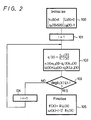
- the nonzero r j (X), by which the polynomials are exactly divided finally, is the greatest common divisor (GCD) of the polynomials r -1 (X), ro(X).
- U i (X), V i -(X) are calculated according to the following equations: In this case, (-1 ) j + 1 V j (X) becomes U(X) and (-1) j U j (X) becomes V(X).
- r -1 (X) and ro(X) are initialized into X 2t and S(X), respectively, and U -1 (X) and U o (X) are initialized into 0 and 1, respectively.
- the number i of steps is set to 1.
- the number i of steps is incremented by 1, and control returns to the step 102.
- a multiple of U i (X) by a becomes the error locator polynomial a(X), and a multiple of r i (X) by (-1) i ⁇ becomes the error evaluator polynomial ⁇ (X).
- a is a constant for equalizing ao (the Oth coefficient of the equation (8)) to 1.
- (-1) i can also be 1.
- FIG. 3 shows a hypothetical circuit (which is a specific circuit arrangement for the conventional error locator polynomial deriving circuit 2 shown in FIG. 1) for executing the algorithm shown in FIG. 2.
- the circuit shown in FIG. 3 comprises mutual division units 8A through 8Z which are identical in construction to each other, the mutual division units 8A through 8Z including respective main calculating units 9A through 9Z for calculating q i (X) and r i (X) in the step 102 shown in FIG. 2, and respective auxiliary calculating circuits 10A through 10Z for calculating U i (X).
- ro(X) S(X), U -1 (X), U 0 (X) of the functions r i (X), U i (X), these functions change successively into (ro(X), ri (X), Uo(X), U 1 (X)), (r 1 (X), r 2 (X), U 1 (X), U 2 (X)), ⁇ , each time they pass through one division circuit.
- the last mutual division unit 8Z produces ⁇ (X) and ⁇ (X).
- Ro(X), Qo(X), ⁇ 0 -(X), ⁇ 0 (X), ⁇ 0(X), and ⁇ 0(X) are initialized into X 2t , S(X), 0, 1, 1, and 0, respectively.
- the number i of steps is set to 1.
- the difference l i-1 between the degree of R i-1 (X) and the degree of Q i-1 (X) is determined, and the coefficients of the greatest-power terms of R i-1 (X) and Q i-1 (X) are set to a i-1 and b i-1 , respectively.
- This step is executed if l i-1 ⁇ 0, i.e., the degree of R i-1 (X) is greater than the degree of Q i-1 (X).
- R i (X), ⁇ i -(X), ⁇ i(X) are calculated according to the following equations:
- the division R i-1 (X)/Q i-1 (X) is replaced with the division a i-1 /b i-1 between the coefficients of the greatest-power terms.
- This step is executed if l i-1 ⁇ 0, i.e., the degree of R i-1 (X) is less than the degree of Q i-1 (X).
- R i (X), ⁇ i (X), ⁇ i (X) are calculated according to the following equations:
- R i-1 (X) and Q i-1 (X) are exchanged.
- the number i of steps is incremented by 1, and control returns to the step 108.
- ⁇ i (X) and R(X) are regarded respectively as the error locator polynomial o(X) and the error evaluator polynomial ⁇ (X). In this case, i is 2t.
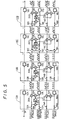
- FIG. 5 shows a specific circuit arrangement for the conventional improved error locator polynomial deriving circuit 2 for executing the algorithm shown in FIG. 4.
- the circuit shown in FIG. 5 comprises mutual division units 11 A through 11Z which are identical in construction to each other.
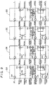
- the first mutual division unit 11 A for example, has a pair of switch circuits 12A, 13A and another pair of switch circuits 14A, 15A. Input ports of these switch circuits 12A through 15A are supplied with the coefficients of R o (X), Q o (X), ⁇ 0 (X), and ⁇ 0 (X).
- the switch circuits 12A through 15A deliver the supplied coefficients directly to their output ports as they are. If to is negative, the switch circuits 12A, 13A operate so as to be connected in crossed relation to each other, and the switch circuits 14A, 15A operate so as to be connected in crossed relation to each other.
- the coefficients appearing at the output port of the switch circuit 12A are supplied to a dividend input port of a divider 19A and one input port of an adder 20A, and the coefficients appearing at the output port of the switch circuit 13A are supplied to a divisor input port of the divider 19A and one input port of a multiplier 23A.
- the quotient produced at first by the divider 19A is supplied through a data holding register 22A to another input port of the multiplier 23A, whose output is supplied to another input port of the adder 20A.
- the coefficients appearing at the output ports of the switch circuits 14A, 15A are supplied respectively to one input port of an adder 21 A and one input port of a multiplier 24A.
- the coefficients held by the register 22A are supplied to another input port of the multiplier 24A, whose output is supplied to another input port of the adder 21 A.
- the adders, multipliers, and dividers shown in FIG. 5 effect arithmetic operations between the elements of the finite field GF(2 m ).
- the mutual division unit 11 A also includes delay registers 16A, 17A, 18A each comprising a D-type flip- flop.
- the coefficients appearing at the output ports of the switch circuits 13A, 15A are supplied as the coefficients of the polynomials Q 1 (X) and ⁇ 1 (X) through the respective registers 17A, 18A to the next mutual division unit 11 B.
- the coefficients appearing at the output ports of the adders 20A, 21 A are supplied as the coefficients of the polynomials R 1 (X) and ⁇ 1 (X) to the next mutual division unit 11 B.
- the other mutual division units 11 B, 11 C, 11 D also generate the coefficients of the polynomials R i (x), Q i (X), x(X), ⁇ 1 (X) from the coefficients of the supplied polynomials R i-1 (X), Q i-1 (X), ⁇ i-1 (X), ⁇ i-1 (X) in synchronism with the start flag signal SF.
- the coefficients of Ro(X) and ⁇ 0 (X) are supplied to the mutual division unit 11A successively from those of the greatest-power terms (X 4 ), the coefficients of Q o (X) and ⁇ 0 (X) are supplied to the division unit 11A successively from those of the greatest-power terms (X 3 ), and the start flag signal SF is set to a high-level "1" " in synchronism with the coefficients of the greatest-power terms.
- an error locator polynomial can accurately be derived in principle.
- control proceeds to the normal mode in the step 110 even when l i-1 ⁇ 0.
- the degree of R i (X) can be reduced only one at a time in principle according to the Euclidean division algorithm, the number of division units 11 A, 11B, ⁇ shown in FIG. 5 is required to be 2t for those codes whose t error symbols can be corrected.
- the Reed-Solomon code is employed, the correction of 3 symbols has already been achieved at present for those applications, such as digital VTRs, in which real-time processing is required (with the clock frequency being about 15 MHz), and the correction of 8 symbols has already been achieved at present for those applications, such as optical disc players, in which real-time processing is not required.
- a decoder for decoding multiple error-correcting codes where the number t of symbols whose errors can be corrected is about 16 with respect to the code length n of about 160.
- Another object of the present invention is to provide a finite field multiplication circuit of small size for multiplying the same number over a finite field GF(2 m ) by respective different numbers over the finite field GF(2 m ) simultaneously and in parallel relationship.
- Still another object of the present invention is to provide a finite field division circuit of small size for effecting divisions over a finite field GF(2 m ).
- a mutual division circuit comprising a single mutual division unit or a plurality of cascaded mutual division units for dividing a polynomial including a first input polynomial R i - 1 (X) as a factor by a second input polynomial Q i-1 (X), thereby to determine a quotient and a remainder R(X), determining an overall quotient ⁇ i (X) from the quotient and a third input polynomial ⁇ i-1 (X), and producing the remainder R i (X), the first input polynomial R i-1 (X) or the second input polynomial Q i-1 (X), and the overall quotient ⁇ i (X) as a first output polynomial R i (X), a second output polynomial O i (X), and a third output polynomial ⁇ i (X), respectively, data selecting means (42) for receiving, at an input port thereof, respective initial polynomials of the
- a multiplication circuit for a finite field comprising conversion means (101) for converting a number in an m-bit vector representation over a finite field GF(2 m ) into elements of a matrix representation, and multiplication means (102, 103, 104) for multiplying the elements of the matrix representation from the conversion means (101) by a plurality of numbers in respective m-bit vector representations over the finite field GF(2 m ) in parallel relationship, to produce a plurality of products in respective vector representations over the finite field GF(2 m ).
- a division circuit for a finite field comprising an inverse element generating circuit (203) for generating a vector representation of the inverse element of a first element in an m-bit vector representation over a finite field GF(2 1 ), and a multiplication circuit (202) for multiplying the inverse element by a second element in an m-bit vector representation over the finite field GF(2 m ), with one of the elements being converted into a matrix representation, and dividing the second element by the first element, thereby to produce a quotient in an m-bit vector representation over the finite field OF(2 m ).
- a mutual division unit which is free of the drawbacks of the mutual division units 11 A through 11 D shown in FIG. 5.
- the mutual division unit according to the first embodiment of the present invention will now be described below.
- FIG. 6 shows a mutual division unit 25 which includes delay registers 26, 27, 28.
- the delay registers 26, 27, 28 are supplied with a start flag signal SF, the coefficients of a polynomial Q i-1 (X), and the coefficients of a polynomial ⁇ i-1 (X), respectively.
- the register 26 produces an output signal which is supplied as a start flag signal SFO to a next mutual division unit.
- the mutual division unit 25 also includes switch circuits 29, 30, 31 for transmitting supplied coefficients parallel or in crossed relation to each other.
- the switch circuit 29 has two input ports supplied with variables dR i-1 , dQ i-1 which indicate the degrees of respective polynomials.
- the switch circuit 30 has two input ports supplied with the coefficients of the polynomial R i-1 (X) and the coefficients produced by the register 27.
- the coefficients which appear at one output port of the switch circuit 30 are supplied to a dividend input port of a divider 30 and one input port of an adder 34.
- the coefficients which appear at the other output port of the switch circuit 30 are supplied to a divisor input port of the divider 33 and one input port of a multiplier 37.
- the input ports of the switch circuit 31 are supplied with the coefficients of a polynomial ⁇ i-1 (X) and the coefficients produced by the register 28, respectively.
- the coefficients appearing at the output ports of the switch circuit 31 are supplied to one input port of an adder 35 and one input port of a multiplier 38, respectively.
- the quotient produced by the divider 33 is held by a register 36, and then supplied to other input terminals of the multipliers 37, 38, respectively.
- the output data from the multipliers 37, 38 are supplied respectively to other input ports of the adders 34, 35.
- the coefficients of polynomials R(X), Q i (X), ⁇ i (X), and ⁇ i (X) are supplied from the output port of the adder 34, the other output port of the switch circuit 30, the output port of the adder 35, and the other output port of the switch circuit 31, respectively, to the next mutual division unit.
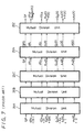
- FIG. 7 A circuit arrangement in which 2t mutual division units 25A through 25Z, each identical in construction to the mutual division unit 25 shown in in FIG. 6, are connected in cascade is illustrated in FIG. 7.
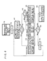
- Ro(X), Qo(X), xo(X), ⁇ 0 (X), dRo, and dQo are initialized into a syndrome polynomial S(X), X 2t , 1, 0, 2t-1, and 2t, respectively.
- the step 115 differs from the step 106 of the algorithm shown in FIG. 4 partly in that the initial values for Ro(X) and Qo(X) are exchanged with each other and the initial values for Xo(X) and ⁇ 0 -(X) are exchanged with each other.
- the number i of steps is set to 1.
- the difference l i-1 between dR i-1 and dQ i-1 is determined, and the coefficient of the dR i-1 th term of R i-1 -(X) and the coefficient of the dQ i-1 th term of Q i-1 (X) are set to a i . 1 and b i-1 , respectively. Since the coefficient of the greatest-power term of the syndrome polynomial S(X) which is Ro(X) can be 0 in this case, the coefficient a i-1 may be 0.
- This step is executed if l i-1 ⁇ 0, i.e., dR i-1 (X) is greater than dQ i-1 (X).
- R i (X), ⁇ i (X) are calculated according to the following equations:
- control goes through the step 121 to the step 123. If a i-1 is not 0, then control goes through the step 122 to the step 123.
- This step is executed if the degree of Q i-1 (X) is greater than the degree of R i-1 (X), and the coefficient a i-1 is not 0.
- R i-1 (X) and Q i-1 (X) in the Normal mode are exchanged, and R i (X) and ⁇ i (X) are calculated according to the following equations:
- control goes to the step 123.
- This step is executed if the coefficient a i-1 of the dR i-1 th term (greatest-power term) of R i (X) is 0 and the actual degree of R i-1 (X) is less than (dR i-1 - 1).
- R i-1 (X) is multiplied by X to shift R i-1 (X) to a higher degree, so that divisions by R i-1 (X) are made possible.
- This step determines whether the number i of steps has reached 2t or not. If not, then control goes to the step 124. If the number i of steps has reached 2t, then control goes to the final step 125.
- the operation sequence of the steps 117 through 123 is always repeated 2t times in the overall error locator polynomial deriving circuit.
- each mutual division unit executes the steps 117 through 123 only once.
- dR 2t represents a number produced by subtracting 1 from the degree ⁇ of the error locator polynomial ⁇ (X).
- both ⁇ 2t (X) and R 2t (X) need to be shifted to a lower degree using a shift polynomial P(X), described later, in order to obtain a(X) and ⁇ (X).
- the number i of steps is incremented by 1, and control returns to the step 117.
- the syndrome polynomial S(X) is expressed by the equation (22), and the variables and the initial values of the polynomials in the step 115 shown in FIG. 8 are as follows:
- the coefficients of Ro(X) ⁇ ⁇ 0 (X) are supplied to the mutual division unit 25A successively from those of the greatest-power terms, the values of dR o and dQ o are supplied to the mutual division unit 25A, and the start flag signal SF is set to a high-level "1" in synchronism with the coefficients of the greatest-power terms.
- the code length n is 150 and the number t of error-correctable symbols is 16.
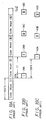
- the operation sequence of the steps 117 through 123 shown in FIG. 8 is required to be repeated 32 (2t) times. If the mutual division units are simply connected in cascade as is conventional, then 32 mutual division units 25 shown in FIG. 6 are necessary. If the transmitted code word is transmitted one symbol at a time in synchronism with clock pulses CK, and if one period of the clock pulses CT is 1Tc, then 150 received code words I, II, III, ⁇ are transmitted in a period 150Tc, as shown in FIG. 10 at A.
- the coefficients of the error locator polynomial a(X) corresponding to the received code words I, II, III, ⁇ are successively produced by the final mutual division unit in respective periods 40A, 40B, 40C, ⁇ , 128Tc after the respective code words I, II, III, ⁇ are received.
- the period IT may be regarded as an idle time. If the number t of error-correctable symbols and the code length N satisfy the relationship N » 2t in general, the simple cascaded connection of the mutual division units results in an increased circuit arrangement size and an extended idle time IT.
- the principles of the invention are applied to an error locator polynomial deriving circuit (corresponding to the circuit 2 in FIG. 1) in a decoder for decoding the Reed-Solomon code, with the code length n being 150 and the number t of error-correctable symbols being 16.
- the error locator polynomial deriving circuit shown in FIG. 11 comprises eight mutual division units each of the construction shown in FIG. 6, each mutual division unit having a data delay time corresponding to 4 clock pulses (4Tc).
- the algorithm used in each of the mutual division units shown in FIG. 11 is the same as the improved Euclidean division algorithm shown in FIG. 8.
- the error locator polynomial deriving circuit shown in FIG. 11 includes a data bus 41, a data selector 42, eight mutual division units 43A through 43H, a delay register 44, and a data bus 45.
- the coefficients of the syndrome polynomial S(X) and the polynomial X 2t are supplied through the data bus 41 to one input port of the data selector 42.
- Each of the mutual division units 43A through 43H is structurally identical to the mutual division unit shown in FIG. 6, as described above.
- the delay register 44 delays data by a delay time corresponding to one clock pulse (1Tc).
- the mutual division units 43A through 43H are connected in cascade between the output port of the data selector 42 and the input port of the delay register 44.
- the data bus 45 connects the output port of the delay register 44 to the other input port of the data selector 42.
- the data bus 45 has a branch output bus 45a for delivering the coefficients of an error locator polynomial ⁇ -(X) and an error evaluator polynomial ⁇ (X), which are finally produced, to a subsequent circuit (not shown).
- the period of 33Tc is required until all the coefficients of S(X), X 2t , as initial values, and the variables are supplied.
- the 33 sets of initial data which are composed of the coefficients of S(X), x 2t are supplied to the first mutual division unit 43A by the data selector 42. From the mutual division unit 43A, there are stored intermediate processed data of the 33 sets of data into the delay register 44.
- the data selector 42 is switched over to supply the data from the delay register 44 to the first mutual division unit 43A.
- the 33 sets of intermediate processed data held between the mutual division unit 43A and the delay register 44 are processed while being shifted once through a loop which comprises the mutual division units 43A through 43H, the delay register 44, the data bus 45, and the data selector 42. Thereafter, as shown in FIG.
- the initial 33 sets of data supplied through the data bus 41 circulate four times through the loop. Since the loop includes the eight mutual division units 43A through 43H, the initial 33 sets of data are passed through a total of 32 mutual division units, so that the coefficients of the error locator polynomial can be determined with accuracy. Although the 32 mutual division units were required in the conventional circuit, the mutual division circuit according to this embodiment only requires eight mutual division units 43A through 43H, the number of which is a quarter of the number of the mutual division units in the conventional circuit. The mutual division circuit according to this embodiment may therefore be much smaller in size.
- This delay time is substantially equal to the delay time 128Tc of the conventional arrangementshown in FIG. 10.
- the idle time IT in this embodiment is a time which is left by subtracting 132Tc from 150Tc, and is much shorter than the idle time shown in FIG. 10.
- the upper limit T u of the time T CK of a clock pulse unit required to process data once in the series of mutual division units (upon one circulation therethrough) is given by:
- the lower limit To for the time T CK is given by: Therefore, from the equation (29), if the number R of times by which the mutual division units are repeatedly used is increased, the number G of mutual division units connected in series may be reduced to 1 at minimum.
- a delay register should be employed in this case in order to keep the delay time T CK in the range of T D ⁇ T CK ⁇ T U .
- the error location polynomial and the error evaluation polynomial may finally be extracted from the mutual division circuit at a junction between adjacent mutual division units (e.g., between the mutual division units 43E, 43F in FIG. 11).
- each of the mutual division units 43A through 43H has a data delay time corresponding to 4 clock pulses (4Tc).
- FIG. 13 shows a specific synchronous arrangement of the mutual division unit whose data delay time is 4Tc. Those parts and signals in FIG. 13 which correspond to those shown in FIG. 6 are denoted by identical reference characters, and will not be described in detail.
- the mutual division unit includes delay registers 51 through 68 comprising D-type flip-flops, respectively, and data selectors 69 through 74 each having two input ports.
- the paired data selectors 69, 70, the paired data selectors 71, 72, and the paired data selectors 73, 74 correspond respectively to the switch circuits 29, 30, 31 shown in FIG. 6.
- the comparison signal REV from the comparator 75 is supplied to one input terminal of an AND gate 77.
- a zero detector 76 produces a zero-detected signal RZ which is of high level "1" only when the coefficients of the polynomial R i-1 (X) are 0.
- the zero-detected signal RZ is supplied to the other negative-logic input terminal of the AND gate 77.
- An output signal from the AND gate 77 is held by the register 58, whose output signal CRS is used to control switching of the data selectors 69 through 74.
- the register 54 is connected to one input terminal of the data selector 71, whose output terminal is connected to the registers 59, 63.
- the registers 55, 56, 57 are connected respectively to input terminals of the data selectors 72, 73, 74, whose output terminals are connected to the registers 60, 64, the registers 61, 65, and the registers 62, 66, respectively.
- a start flag signal SF is converted into flag signals SF1, SF2, SF3, SFO respectively by the registers 26, 51, 52, 53.
- the flag signal SF1 serves to control the register 58
- the flag signal SF3 serves to control the registers 36, 67, 68.
- the other registers are controlled by clock pulses CK.
- the coefficients of the polynomials R i (X) ⁇ ⁇ i (X) are generated 4Tc after the coefficients of the polynomials R i-1 (X) ⁇ ⁇ i-1 (X). Therefore, the delay time of the mutual division unit shown in FIG. 13 is 4Tc.
- the timing chart shown in FIG. 14 is based on the assumption that the division between the elements of a finite field by the divider 33 is finished within 1Tc, and the multiplication and addition between the elements of a finite field by the multiplier 37 and the adder 34 is finished within 1Tc.
- FIGS. 15 through 18 A mutual division unit according to another embodiment of the present invention will be described with reference to FIGS. 15 through 18.
- the mutual division unit shown in FIG. 15 is arranged to consume 2Tc in completing divisions between the elements of a finite field.
- Those parts and signals shown in FIG. 15 which correspond to those shown in FIG. 13 are denoted by identical reference characters, and will not be described in detail.
- a delay register 88 is connected to the output port of the register 53.
- the registers 36, 67, 68 are controlled by a flag signal SF4 produced from the register 53.
- the output port of the data selector 71 is connected through a register 78 to the divider 33, and also connected through registers 79, 80, 59 to the adder 34.
- the output port of the data selector 72 is connected through a register 81 to the divider 33, and also connected through registers 82, 83, 60 to the multiplier 37.
- the registers 78, 81 are controlled by the flag signal SF2.
- registers 84, 85, 61 are connected between the data selector 73 and the adder 35, and registers 86, 87, 62 are connected between the data selector 74 and the multiplier 38.
- FIG. 16 is a timing chart of an operation sequence of the mutual division unit shown in FIG. 15 under the same conditions as those of the mutual division unit shown in FIG. 13. According to the operation sequence shown in FIG. 16, the divisions require an additional 1Tc, and thus the overall delay time is 5Tc.
- FIG. 17 shows a portion of a modification of the mutual division unit shown in FIG. 15.
- pipeline registers 89, 90, 91 are connected between the register 59 and the adder 34, between the register 60 and the output port of the mutual division unit, and between the multiplier 37 and the adder 34, respectively.
- a multiplication and an addition are reliably be carried out in respective one clock cycles.
- FIG. 18 shows a portion of a modification of the mutual division unit shown in FIG. 17.
- a register 94 is connected between the register 89 and the adder 34, and a matrix conversion circuit 92 for converting the representation of the elements of a finite field from a vector representation into a matrix representation, and a register 93 are connected between the register 36 and the multiplier 37.
- a register 95 is connected between the registers 60, 90.
- the modified mutual division unit shown in FIG. 18 is designed to increase the speed of multiplication by incorporating the multiplication system using the matrix representation of a finite field and the pipeline system, as disclosed in Japanese Patent Laid-Open Gazette No. 60-144834.
- the divider 33 is employed in the above embodiment, the divider may be dispensed with, and the mutual division unit may be composed of an increased number of multipliers.
- the present invention since the mutual division units are repeatedly used, the number of mutual division units employed is reduced, and hence the size of the mutual division circuit is also reduced.
- the present invention is particularly useful when the code length n and the number t of error-correctable symbols meet the relationship n » t, the number t being of a relatively large value.
- FIGS. 19 and 20 A mutual division circuit according to another embodiment of the present invention will now be described with reference to FIGS. 19 and 20.
- the principles of the invention are applied to an error locator polynomial deriving circuit (corresponding to the circuit 2 in FIG. 1) in a decoder for decoding the Reed-Solomon code.
- the error locator polynomial deriving circuit shown in FIG. 19 comprises 2t mutual division units each of the construction shown in FIG. 6, each mutual division unit having a data delay time corresponding to 4 clock pulses (4Tc).
- the algorithm used in each of the mutual division units shown in FIG. 19 is the same as the improved Euclidean division algorithm shown in FIG. 8.
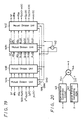
- the error locator polynomial deriving circuit shown in FIG. 19 includes 2t mutual division units 141A through 141 Z which are connected in cascade, each of the mutual division units 141 A through 141 Z being of a structure similar to the structure shown in FIG. 6, except that the divider 33 is dispensed with, and a divider 142 for carrying out divisions between the elements of a finite field GF(2 m ). From each of the mutual division units 141A through 141Z, there extend bus lines for outputting a dividend NML and a divisor DNM and a bus line for inputting a quotient SHO. The dividend NML and the divisor DNM are supplied respectively to dividend and divisor input ports of the divider 142, whose output port is connected to the bus lines which input the quotient to the mutual division units 141 A through 141 Z.
- FIG. 20 shows a specific circuit arrangement of the divider 142 shown in FIG. 19.
- the divider 142 includes an inverse element generating ROM 143, a multiplier 144 for multiplying a matrix by a vector, and an representation conversion circuit 145 for converting the representation of the elements of a finite field from a vector representation into a matrix representation.
- the elements of a dividend x in a vector expression are supplied to an input port of the representation conversion circuit 145, which outputs a matrix representation T(X) of the dividend x.
- the elements of the matrix representation are then supplied to a matrix element input port of the multiplier 144.
- the elements of a divisor y in a vector representation are supplied to an address bus of the inverse element generating ROM 143 which outputs the inverse element y -1 , in a vector representation, of the divisor y over its data bus.
- the elements of the inverse element y- 1 in the vector representation are supplied to a vector element input port of the multiplier 144.
- the matrix representation of the elements of a finite field is disclosed in Japanese Patent Laid-Open Gazette No. 60-144834.
- the inverse element y- 1 of the divisor y is first determined, and the dividend x is multiplied by the inverse element y- 1. Since the inverse element generating ROM 143 and the representation conversion circuit 145 operate parallel to each other, the time required by the division is greatly reduced.
- the divider 142 may comprise a ROM table for determining the exponents i and j of the powers of the dividend x and the divisor y, a subtractor for calculating the exponent i - j, and a ROM table for determining a vector representation ⁇ i-j from the exponent i - j.
- the mutual division circuit shown in FIG. 19 operates as follows:
- the first mutual division unit 141 A is supplied with the initial data indicated in the step 115 shown in FIG. 8.
- the start flag signal SF is set to a high-level "1 " in synchronism with the coefficients of the greatest-power terms of the polynomials in those initial data.
- the mutual division units 141A through 141Z recognize that they are supplied with the coefficients of the greatest-power terms of the polynomials when the start flag signal SF is set to a high-level "1".
- the data processed by the first mutual division unit 141A are supplied to the next mutual division unit 141 B.
- the mutual division unit 141 B When the start flag signal SF supplied to the mutual division unit 141 B is set to a high-level "1", then the mutual division unit 141 B starts to carry out the operation shown in FIG. 8. Similarly, as the start flag signal SF supplied successively to the following mutual division units is successively set to a high-level "1", these mutual division units successively start to effect the operation shown in FIG. 8. Finally, the last mutual division unit 141 Z produces an error locator polynomial a(X) and an error evaluator polynomial W (X).
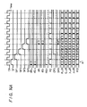
- the timing of divisions in the mutual division units 25A through 25D shown in FIG. 9 will be analyzed in detail below.
- the quotient produced by the division in the divider 33A is held in the register 36A until the coefficients of all the other terms of Ro(X), Qo-(X).
- the divider 33A idles after the division in the period ranging from 1Tc to 2Tc is finished.
- the dividers 33B through 33D in the other mutual division units 25B through 25D also idle while the divisions for the respective mutual division units are not being executed.
- the dividers 33A through 33D are put together into a single divider according to the arrangement shown in FIG. 19.
- the multiplier 23A in the mutual division unit 11A for example, shown in FIG. 5 is required to multiply the quotient U 7 by a new coefficient at all times, and its idling time is short. Therefore, it would be difficult to combine the multipliers 23A through 23D in the mutual division units 11A through 11 D into a single multiplier.
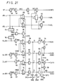
- FIG. 21 A specific circuit arrangement of a mutual division unit for use in the mutual division circuit shown in FIG. 19 is shown in FIG. 21.
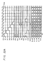
- An operation sequence of the mutual division unit shown in FIG. 21 is illustrated in FIG. 22.
- each of the mutual division units 141A through 141 Z has a data delay time corresponding to 4 clock pulses (4Tc).
- FIG. 21 shows a specific synchronous arrangement of such a mutual division unit whose delay time is 4Tc. Those parts and signals in FIG. 21 which correspond to those shown in FIG. 6 are denoted by identical reference characters, and will not be described in detail.
- the mutual division unit includes delay registers 51 through 68 comprising D-type flip-flops, respectively, and data selectors 69 through 74 each having two input ports.
- the paired data selectors 69, 70, the paired data selectors 71, 72, and the paired data selectors 73, 74 correspond respectively to the switch circuits 29, 30, 31 shown in FIG. 6.
- the comparison signal REV from the comparator 75 is supplied to one input terminal of an AND gate 77.
- a zero detector 76 produces a zero-detected signal RZ which is of high level "1" only when the coefficients of the polynomial R i-1 (X) are 0.
- the zero-detected signal RZ is supplied to the other negative-logic input terminal of the AND gate 77.
- An output signal from the AND gate 77 is held by the register 58, whose output signal CRS is used to control switching of the data selectors 69 through 74.
- the register 54 is connected to one input terminal of the data selector 71, whose output terminal is connected to the registers 59, 63.
- the registers 55, 56, 57 are connected respectively to input terminals of the data selectors 72, 73, 74, whose output terminals are connected to the registers 60, 64, the registers 61, 65, and the registers62, 66, respectively.
- Output data A from the register 59 are extracted as a dividend NML through a buffer 146
- output data from the register 60 connected to the output terminal of the data selector 72 are extracted as a divisor DNM through a buffer 147.
- the buffers 146, 147 provide a high impedance at their output terminals when they are not strobed.
- a start flag signal SF is converted into flag signals SF1, SF2, SF3, SFO respectively by the registers 26, 51, 52, 53.
- the flag signal SF1 serves to control the register 58
- the flag signal SF3 serves to control the registers 136, 67, 68.
- the other registers are controlled by clock pulses CK.
- Signals generated in the mutual division unit are denoted by reference characters in FIG. 21. If it is assumed that the variables dRo, dQo and the polynomials Ro(X) ⁇ ⁇ 0 (X) supplied to the mutual division unit 25A shown in FIG. 9 are used as the variables dR i - 1 , dQ;.
- the coefficients of the polynomials R i (X) ⁇ ⁇ i (X) are generated 4Tc after the coefficients of the polynomials R i-1 (X) ⁇ ⁇ i-1 (X). Therefore, the delay time of the mutual division unit shown in FIG. 21 is 4Tc.
- the timing chart shown in FIG. 22 is based on the assumption that the division between the elements of a finite field by the divider 142 is finished within 1Tc, and the multiplication and addition between the elements of a finite field by the multiplier 37 and the adder 34 is finished within 1Tc.
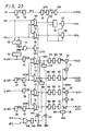
- a mutual division unit according to another embodiment of the present invention will be described with reference to FIGS. 23 and 24.
- the mutual division unit shown in FIG. 23 is arranged to consume 2Tc in completing divisions between the elements of a finite field.
- Those parts and signals shown in FIG. 23 which correspond to those shown in FIG. 21 are denoted by identical reference characters, and will not be described in detail.
- a delay register 188 is connected to the output port of the register 53.
- the registers 136, 67, 68 are controlled by a flag signal SF4 produced from the register 53.
- the output port of the data selector 71 is connected through a register 178 to the buffer 147, and also connected through registers 179, 180, 59 to the adder 34.
- the output port of the data selector 72 is connected through a register 181 to the buffer 146, and also connected through registers 182, 183, 60 to the multiplier 37.
- the registers 178, 181 are controlled by the flag signal SF2.
- the buffers 146, 147 are controlled by the flag signals SF2, SF3 through an OR gate 148 having two input terminals and a register 149.
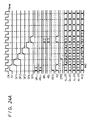
- FIG. 24 is a timing chart of an operation sequence of the mutual division unit shown in FIG. 23 under the same conditions as those of the mutual division unit shown in FIG. 21. According to the operation sequence shown in FIG. 24, the divisions require an additional 1Tc, and thus the overall delay time is 5Tc.
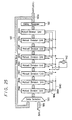
- FIGS. 25 and 26 A mutual division circuit according to still another embodiment of the present invention will now be described with reference to FIGS. 25 and 26.
- the principles of the invention are applied to an error locator polynomial deriving circuit (corresponding to the circuit 2 in FIG. 1) in a decoder for decoding the Reed-Solomon code, with the code length n being 150 and the number t of error-correctable symbols being 16.
- the error locator polynomial deriving circuit shown in FIG. 25 comprises eight mutual division units each of the construction shown in FIG. 21, each mutual division unit having a data delay time corresponding to 4 clock pulses (4Tc).
- the algorithm used in each of the mutual division units shown in FIG. 25 is the same as the improved Euclidean division algorithm shown in FIG. 8.
- the error locator polynomial deriving circuit shown in FIG. 25 includes a data bus 189, a data selector 190, eight mutual division units 191A through 191H, a delay register 192, and a data bus 193.
- the coefficients of the syndrome polynomial S(X) and the polynomial X 2t are supplied through the data bus 189 to one input port of the data selector 190.
- Each of the mutual division units 191A through 191H is structurally identical to the mutual division unit shown in FIG. 21, as described above.
- the delay register 192 delays data by a delay time corresponding to one clock pulse (1Tc).
- the mutual division units 191A through 191 H are connected in cascade between the output port of the data selector 190 and the input port of the delay register 192.
- the data bus 193 connects the output port of the delay register 192 to the other input port of the data selector 190.
- the data bus 193 has a branch output bus 193a for delivering the coefficients of an error locator polynomial a(X) and an error evaluator polynomial w(X), which are finally produced, to a subsequent circuit (not shown).
- the error locator polynomial deriving circuit shown in FIG. 25 also includes a single divider 142 which is shared by the mutual division units 191 A through 191 H, as with the arrangement shown in FIG. 19.
- the period of 33Tc is required until all the coefficients of S(X), X 2t , as initial values, and the variables are supplied.
- the data selector 190 is switched over to supply the data from the delay register 192 to the first mutual division unit 191A.
- the 33 sets of intermediate processed data held between the mutual division unit 191A and the delay register 192 are processed while being shifted once through a loop which comprises the mutual division units 191 A through 191H, the delay register 192, the data bus 193, and the data selector 190. Thereafter, as shown in FIG.
- the initial 33 sets of data supplied through the data bus 189 circulate four times through the loop. Since the loop includes the eight mutual division units 191A through 191 H, the initial 33 sets of data are passed through a total of 32 mutual division units, so that the coefficients of the error locator polynomial can be determined with accuracy. Although the 32 mutual division units were required in the conventional circuit, the mutual division circuit according to this embodiment only requires eight mutual division units 191 A through 191H, the number of which is a quarter of the number of the mutual division units in the conventional circuit. The mutual division circuit according to this embodiment may therefore be much smaller in size.
- This delay time is substantially equal to the delay time 128Tc of the conventional arrangement shown in FIG. 10.
- the idle time IT in this embodiment is a time which is left by subtracting 132Tc from 150Tc, and is much shorter than the idle time shown in FIG. 10.
- the upper limit T u of the time T CK of a clock pulse unit required to process data once in the series of mutual division units (upon one circulation therethrough) is given by:
- the lower limit To for the time T CK is given by: Therefore, from the equation (33), if the number R of times by which the mutual division units are repeated used is increased, the number G of mutual division units used in series may be reduced to 1 at minimum.
- a delay register should be employed in this case in order to keep the delay time T CK in the range of T D ⁇ T CK ⁇ T U .
- the divider 142 shown in FIG. 25 effects respective for the mutual division units 191 A through 191 H successively in the periods 94A through 94D shown in FIG. 26, and then effects respective divisions for the mutual division units 191 A through 191H successively in the following periods 95A through 95H. Therefore, even with the mutual division units 191A through 191H being repeatedly used as shown in FIG. 25, the timings at which the divider 142 is used by the mutual division units 191 A through 191 H for their divisions do not interfere with each other.
- the timings can easily be adjusted out of mutual interference by adjusting the delay time in the delay register 192.
- the timings at which the divider is used by the mutual division units may be brought into mutual interference when different syndrome polynomials S(X) are successively processed.
- a delay register for adjusting the delay time may be connected between the mutual division units.
- Error-correcting codes such as the Reed-Solomon code, the concatenated code, etc. are used in practice when digital audio and video signals are recorded and reproduced. Encoders for encoding these error-correcting codes generate parity data (redundant data). Decoders for decoding the error-correcting codes generate a syndrome from a received signal which contains parity data, and correct errors using the syndrome.
- Each of a parity generator, a syndrome generator, and an error-correcting circuit comprises an arithmetic circuit for a finite field (Galois field) GF(p m ) of order p m .
- Arithmetic circuits over the finite field GF(2m) include an addition circuit (which is of the same construction as a subtraction circuit over GF(2 m ), a multiplication circuit, and a division circuit.
- the addition circuit can simply be composed of exclusive-OR gates.
- the multiplication and division circuits are complex in construction.
- One known multiplication circuit employs a ROM as a conversion table. If it is assumed that a root of the irreducible polynomial of the finite field GF(2 m ) is represented by a when the irreducible polynomial is 0, the elements of this finite field, except for 0, are expressed by powers of a.
- a' is inputted to the ROM to obtain an exponent i
- a i is inputted to the ROM to obtain an exponent j
- the exponent (i + j) is produced by an addition circuit
- the exponent (i + j) is inputted to the ROM, which then outputs ⁇ i+j .
- Another multiplication circuit employs a matrix expression of each of the elements of a finite field, thus omitting any ROM.
- a multiplication circuit for effecting such multiplications includes a plurality of identical multipliers arranged parallel to each other.
- Each of the multipliers is relatively large in size. Therefore, the multiplication circuit with the parallel-connected multipliers is considerably large in size, and cannot be incorporated in various products which are required to be reduced in size. The large-size multiplication circuit is also expensive to manufacture.
- the present invention provides a multiplication circuit of small size for multiplying different numbers (multiplicands) over the finite field GF(2 m ) by the same number (multiplicator) over the finite field GF(2 m ) at the same time and in parallel relationship.
- One known division circuit employs a ROM as a conversion table. If it is assumed that a root of the irreduciblepolynomial of the finite field GF(2 m ) is represented by a when the irreducible polynomial is 0, the elements of this finite field, except for 0, are expressed by powers of a.
- a' is inputted to the ROM to obtain an exponent i
- ⁇ j is inputted to the ROM to obtain an exponent j
- the exponent (i - j) is produced by a subtraction circuit
- the exponent (i - j) is inputted to the ROM, which then outputs ⁇ i-j .
- Another multiplication circuit employs a matrix expression of each of the elements of a finite field, thus omitting any ROM.
- a division circuit for effecting such divisions includes a plurality of identical dividers arranged parallel to each other.
- the division circuit with the parallel-connected dividers is considerably large in size.
- the present invention also provides a division circuit of small size for simultaneously effecting a plurality of divisions over the finite field GF(2 m ) with the same multiplicator or multiplicand employed in each of the divisions.
- a representation composed of a vertical column of the coefficients ao through a3 in the equation (39) is referred to as a vector representation of the elements a.
- the vector representation a of the elements a is expressed, using a transposition symbol ( ⁇ ) t , as follows:
- the elements a except 0 over GF(2 4 ) can be represented by ⁇ i .
- the matrix representation T( ⁇ i ) of the elements ⁇ i is defined, using the vector representation ⁇ i a of ⁇ i , by the following equation: Specifically, the matrix representation T( ⁇ 1 ) of a 1 is as follows:
- vector representations are used in actual logic circuits.
- ⁇ j can be expressed by a linear combination of 1, ⁇ , ⁇ 2 , a3, as follows: ⁇ i , i.e., a, is expressed by the equation (39) above.
- the product a ⁇ b is converted into its vector representation as follows: Consequently, when a or ⁇ j is converted into its matrix representation T(a'), the vector representation of the product a'b can easily be determined simply by effecting ordinary multiplication between a matrix and a vector.
- a multiplication circuit for a finite field will now be described below.
- the present invention is applied to a multiplication circuit for multiplying the elements b, c, d over a finite field GF(2) by the common element a over the finite field GF-(2 4 ).
- the modulus polynomial P(X) of the finite field is defined according to the equation (36), using the coefficients g 1 , g, g 3 , and input and output data are given in vector representations using 4-bit binary notations.
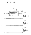
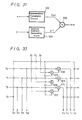
- FIG. 27 shows in block form a multiplication circuit according to the present invention.
- the multiplication circuit includes a representation conversion circuit 101 for converting a vector representation into a matrix representation.
- the representation conversion circuit 101 is supplied with a multiplicator in a 4-bit vector representation and coefficients gi through g 3 (collectively referred to as g) of the modulus polynomial P(X), and generates elements T ij (0 ⁇ i, j ⁇ 3) of the matrix representation T(a) of the multiplicator a.
- the multiplication circuit also has three multiplication units 102, 103, 104 each for multiplying a matrix by a vector.
- the multiplication units 102, 103, 104 are supplied with the elements of the matrix T(a) at one input ports thereof, and multiplicands b, c, d in 4-bit vector representations at the other input ports.
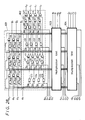
- FIG. 28 shows a specific circuit arrangement of the multiplication circuit shown in FIG. 27.
- the representation conversion circuit 101 shown in FIG. 28 comprises AND gates 105 through 107, 111 through 113, 117 through 119, and exclusive-OR (EXOR) gates 108 through 110, 114 through 116, 120 through 122.
- Each of the AND gates is used as a multiplier for two coefficients, and each of the EXOR gates is used as a mod 2 adder for two coefficients.
- the common coefficient a3 is supplied to one input terminal of each of the AND gates 105, 106, 107, the coefficients g 1 , g 2 , g 3 are supplied respectively to the other input terminals of the AND gates 105, 106, 107, the coefficients ao, a 1 , a 2 are supplied respectively to one input terminals of the EXOR gates 108, 109, 110, and the output data from the AND gates 105, 106, 107 are supplied respectively to the other input terminals of the EXOR gates 108, 109, 110.
- the matrix representation T(a) of the multiplicator a is expressed by the equation (41).
- the coefficients ao through a3 correspond respectively to the elements Too through T 03 of the matrix T(a)
- the coefficient a3 and the output data from the EXOR gates 108, 110 correspond respectively to the element T 1 and the elements T 11 through T 13 of the matrix T(a).
- the output data (the element T 13 ) from the EXOR gate 110 are supplied to one input terminal of each of the AND gates 111 through 113, the coefficients g 1 , g 2 , g 3 are supplied respectively to the other input terminals of the AND gates 111 through 113, the coefficients T 1 through T 1 are supplied respectively to one input terminals of the EXOR gates 114 through 116, and the output data from the AND gates 111 through 113 are supplied respectively to the other input terminals of the EXOR gates 114 through 116.
- the element T 13 and the output data from the EXOR gates 114 through 116 correspond respectively to the elements T 20 and T 21 through T 23 of the matrix T(a), and the element T 23 and the output data from the EXOR gates 120 through 122 correspond respectively to the element T 30 and the elements T 31 through T 33 of the matrix T(a).
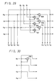
- FIG. 29 shows the AND gates 105 through 107 (FIG. 28) as multipliers and the EXOR gates 108 through 110 (FIG. 28) as adders.
- the vector representation of the element ⁇ i+1 is (as, ao + a 3 gi, a 1 + a 3 g 2 , a 2 +a 3 g 3 ) t , which corresponds to (T 10 T 11 T 12 T 13 ) t . Since the coefficients of the respective output data from the adders 108, 109, 110 are ao + a 3 g 1 , a 1 + asg 2 , a 2 + a 3 g 3 ,the elements T 10 through T 13 of the matrix T(a) are determined by the arrangement shown in FIG. 29.
- the vector representation (the matrix elements T 20 through T 23 ) of the element ⁇ i+2 is determined from the vector representation of the element ⁇ i+1
- the vector representation (the matrix elements T 30 through T 33 ) of the element a i+3 is determined from the vector representation of the element ⁇ i+2 .
- the multiplication unit 102 is supplied with the elements Too through T 33 of the matrix T(a) generated by the representation conversion circuit 101.
- the multiplication unit 102 includes AND gates 123 through 130, 135 through 142, and EXOR gates 131 through 134, 143 through 150.
- the elements Too through To 3 of the matrix T(a) are supplied respectively to one input terminals of the AND gates 123 through 126, the other input terminals of which are supplied with the coefficient bo in the vector representation of the common multiplicand b.
- the AND gates 123 through 126 produce b 0 T 00 through boTo 3 as their output data.
- the AND gates 127 through 130 when supplied with the remaining coefficients b 1 through b 3 in the vector representation of the multiplicand b, the AND gates 127 through 130 generate b 1 T 10 through b 1 T 13 , the AND gates 135 through 138 generate b 2 T 20 through b 2 T 23 , and the AND gates 139 through 142 generate b 3 T 30 through bsT 3 a.
- the output data from the AND gates 123, 127, 135, 139 are added by way of mod 2 addition by the EXOR gates 131, 143, 147, thus generating a coefficient xo.
- the output data from the AND gates 124, 128, 136, 140 are added by way of mod 2 addition by the EXOR gates 132, 144, 148, thus generating a coefficient x 1 .
- the output data from the AND gates 125, 129, 137, 141 are added by way of mod 2 addition by the EXOR gates 133, 145, 149, thus generating a coefficient x 2 .
- the output data from the AND gates 126, 130, 138, 142 are added by way of mod 2 addition by the EXOR gates 134, 146, 150, thus generating a coefficient x 3 .
- the vector representation of the product x of the multiplicator and the multiplicand a is (xo x 1 x 2 x 3 ) t .
- the coefficient xo for example, is given by:
- the xo calculated by the multiplication unit 102 shown in FIG. 28 satisfies the equation (52).
- the coefficients x 1 through x 3 also satisfy the equation (51).
- the multiplication units 103, 104 shown in FIG. 28 are identical in construction to the multiplication unit 102.
- the multiplication unit 103 is supplied with the elements of the matrix T(a) and the coefficients co through c 3 of the vector representation of the multiplicand c
- the multiplication unit 104 is supplied with the elements of the matrix T(a) and the coefficients do through d 3 of the vector representation of the multiplicand d.
- the multiplication unit 103 outputs the coefficients y o through y 3 of the vector representation of the product y, and the multiplication unit 104 outputs the coefficients z o through z 3 of the vector representation of the product z.
- the multiplication circuit can determine the vector representations of the products x, y, z of the common multiplicator a in the vector representation over the finite field GF(2 4 ) and the different multiplicands b, c, d in the vector representations over the finite field GF(24-).
- the representation conversion circuit 101 is shared by the multiplication units 102, 103, 104, and hence the overall multiplication circuit shown in FIGS. 27 and 28 is relatively small in size.
- any ROM as a conversion table for determining the power i from the element a i over GF(2 4 ), for example, is not required, and all the circuit components comprise AND gates and EXOR gates, the multiplication circuit is easy to control, can effect calculations at high speed, and is inexpensive to manufacture.
- the principles of the present invention are not limited to the illustrated multiplication circuit, but are also applicable to a multiplication circuit for a general finite field GF(2 m ).
- the representation conversion circuit for converting a vector representation into the elements of a matrix representation because the overall circuit size is reduced. As any ROM as a conversion table is not required, it is easy to control the multiplication circuit and the speed of calculations effected thereby is high.
- a division circuit for a finite field according to an embodiment of the present invention will now be described below.
- the modulus polynomial P(X) of the finite field is defined according to the equation (53), using the coefficients gi, g 2 , g 3 , and input and output data are given in vector representations using 4-bit binary notations.
- FIG. 31 shows in block form a division circuit according to the present invention.
- the division circuit includes a representation conversion circuit 201 for converting a vector representation into a matrix representation.
- the representation conversion circuit 201 is supplied with a dividend x in a 4-bit vector representation and coefficients gi through g 3 (collectively referred to as g) of the modulus polynomial P(X), and generates elements T ij (0 ⁇ i, j ⁇ 3) of the matrix representation T(x) of the dividend x.
- the division circuit also has a multiplication unit 202 for multiplying a matrix by a vector thereby to generate a vector, and an inverse element generating ROM as a conversion table for converting the divisor y in a vector representation into an inverse element y -1 in a vector representation.
- One input terminal of the multiplication unit 202 is supplied with the elements of the matrix T(x), and the other input terminal thereof is supplied with the 4-bit coefficients (y -1 ) 0 , (y -1 ) 2 , (y -1 ) 3 of the inverse element y- 1 in the vector representation.
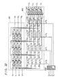
- FIG. 32 shows a specific circuit arrangement of the division circuit shown in FIG. 31.
- the representation conversion circuit 201 shown in FIG. 32 comprises AND gates 205 through 207, 211 through 213, 217 through 219, and exclusive-OR (EXOR) gates 208 through 210, 214 through 216, 220 through 222.
- Each of the AND gates is used as a multiplier for two coefficients, and each of the EXOR gates is used as a mod 2 adder for two coefficients.
- the common coefficient x 3 is supplied to one input terminal of each of the AND gates 205, 206, 207, the coefficients g 1 , g 2 , g 3 are supplied respectively to the other input terminalsof the AND gates 205, 206, 207, the coefficients x o , x 1 , x 2 are supplied respectively to one input terminals of the EXOR gates 208, 209, 210, and the output data from the AND gates 205, 206, 207 are supplied respectively to the other input terminals of the EXOR gates 208, 209, 210.
- the matrix representation T(x) of the multiplicator a is expressed by the equation (41).
- the coefficients xo through x 3 correspond respectively to the elements Too through To 3 of the matrix T(x)
- the coefficient x 3 and the output data from the EXOR gates 208, 210 correspond respectively to the element T 1 and the elements T 11 through T 1 of the matrix T(x).
- the output data (the element T 13 ) from the EXOR gate 210 are supplied to one input terminal of each of the AND gates 211 through 213, the coefficients g 1 , g 2 , g 3 are supplied respectively to the other input terminals of the AND gates 211 through 213, the coefficients T 10 through T 12 are supplied respectively to one input terminals of the EXOR gates 214 through 216, and the output data from the AND gates 211 through 213 are supplied respectively to the other input terminals of the EXOR gates 214 through 216.
- the element T 13 and the output data from the EXOR gates 214 through 216 correspond respectively to the elements T 20 and T 21 through T 23 of the matrix T(x), and the element T 23 and the output data from the EXOR gates 220 through 222 correspond respectively to the element T 3 o and the elements T 31 through T 33 of the matrix T(x).
- FIG. 33 shows the AND gates 205 through 207 (FIG. 32) as multipliers and the EXOR gates 208 through 210 (FIG. 32) as adders.
- the vector representation of the element ⁇ i+1 is ( X3 , xo + x 3 g 1 , x 1 + x 3 g 2 , x 2 + X3 g 3 ) t , which corresponds to (Ti 10 T 11 T 12 T 13 ) t . Since the coefficients of the respective output data from the adders 208, 209, 210 are xo + x 3 g 1 , x 1 + x 3 gz, X2 + X3 g 3 , the elements T 10 through T 13 of the matrix T(x) are determined by the arrangement shown in FIG. 33.
- the vector representation (the matrix elements T 20 through T 23 ) of the element ⁇ i+2 is determined from the vector representation of the element ⁇ i+1
- the vector representation (the matrix elements T 30 through T 33 ) of the element a i+3 is determined from the vector representation of the element ⁇ i+2 .
- the modulus polynomial P(x) may be x 4 + x + 1, for example.
- the multiplication unit 202 is supplied with the elements Too through T 33 of the matrix T(x) generated by the representation conversion circuit 201.
- the multiplication unit 202 includes AND gates 223 through 230, 235 through 242, and EXOR gates 231 through 234, 243 through 250.
- the elements Too through T 03 of the matrix T(x) are supplied respectively to one input terminals of the AND gates 223 through 226, the other input terminals of which are supplied with the coefficient (y -1 ) 0 in the vector representation of the inverse element y- 1 of the divisor y.
- the AND gates 223 through 226 produce (y -1 ) 0 T 00 through (y -1 ) 0 T 03 as their output data.
- the AND gates 227 through 230 generate (y -1 ) 1 T 10 through (y -1 ) 1 T 13
- the AND gates 235 through 238 generate (y -1 ) 2 T 20 through (y -1 )- 2 T 23
- the AND gates 239 through 242 generate (y -1 ) 3 T 30 through (y -1 ) 3 T 33 .
- the output data from the AND gates 223, 227, 235, 239 are added by way of mod 2 addition by the EXOR gates 231, 243, 247, thus generating a coefficient zo.
- the output data from the AND gates 224, 228, 236, 240 are added by way of mod 2 addition by the EXOR gates 232, 244, 248, thus generating a coefficient z 1 .
- the output data from the AND gates 225, 229, 237, 241 are added by way of mod 2 addition by the EXOR gates 233, 245, 249, thus generating a coefficient z 2 .
- the output data from the AND gates 226, 230, 238, 242 are added by way of mod 2 addition by the EXOR gates 234, 246, 250, thus generating a coefficient z 3 .
- the vector representation of the quotient z of the dividend x and the divisor y is (zo z 1 z 2 z 3 ) t .
- the coefficient zo for example, is given by:
- the zo calculated by the multiplication unit 202 shown in FIG. 38 satisfies the equation (58).
- the coefficients z 1 through z 3 also satisfy the equation (57).
- the division circuit determines the vector representation of the quotient z of the dividend x and the divisor y over the finite field GF(2 4 ) by the multiplication of the matrix representation T(x) of the dividend x by the vector representation of the inverse element y- 1 of the divisor y. Since only one ROM (the inverse element generating ROM 203) as a conversion table is needed, the division circuit is smaller in size and the speed of calculations effected thereby is higher than the conventional circuit arrangement which employs three ROMs as conversion tables.
- the representation of the dividend x is converted from the vector representation into the matrix representation.
- the representation conversion circuit 201 may be connected between the inverse element generating ROM 203 and the multiplication unit 202 for converting the representation of the inverse element y- 1 of the divisor y from the vector representation into the matrix representation, and this matrix representation may be multiplied by the vector representation of the dividend x.
- the present invention is also applicable to a division circuit for a general infinite field GF(2m) (m is an integer or 1 or more).
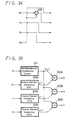
- a division circuit according to a further embodiment of the present invention will be described below with reference to FIG. 35.
- the division circuit includes a representation conversion circuit 201 which is identical in construction to the representation conversion circuit 201 shown in FIG. 31, multiplication units 202A through 202C each identical in construction to the multiplication unit 202 shown in FIG. 31, and inverse element generating ROMs 203A, 203B, 203C each identical in construction to the inverse element generating ROM 203 shown in FIG. 31.
- the representation of the dividend x is converted into a matrix representation T(x) by the representation conversion circuit 201, and the elements of the matrix representation T(x) are supplied to respective one input ports of the multiplication units 202A through 202C.
- the divisors a, c, e are converted into inverse elements a -1 , c- 1 , e- 1 each in a vector representation by the respective inverse element generating ROMs 203A, 203B, 203C, and the inverse elements a -1 , c-1, e- 1 are supplied to the other input ports of the multiplication units 202A, 202B, 202C, respectively. Since each of the multiplication units 202A, 202B, 202C operates in the same manner as the multiplication unit 202 shown in FIG. 31, the multiplication units 202A, 202.B, 202C output respective 4-bit vector representations of the quotients b, d, f.
- the single representation conversion circuit 201 is shared by the three multiplication units 202A through 202C. Therefore, the overall division circuit shown in FIG. 35 is smaller in size than would be if three dividers were simply arranged parallel to each other.
- representation conversion circuits for converting a vector representation into a matrix representation may be connected respectively between the inverse element generating ROMs 203A through 203C and the multiplication units 202A through 202C.
- common dividend x is supplied to the division circuit shown in FIG. 35
- the principles of the present invention are also applicable to a division circuit in which a plurality of dividends are divided by a common divisor. If a common divisor is employed, then it is supplied through an inverse element generating ROM and a representation conversion circuit to a plurality of multiplication units.
- the division circuit according to the present invention is relatively small in size and high in calculation speed.
- the multiplication circuit is arranged to convert the representation of a second element into a matrix representation, then the conversion of the representation of the second element and the generation of the inverse element of a first element are carried out at the same time. Accordingly, calculations can be effected at much higher speed.
Landscapes
- Engineering & Computer Science (AREA)
- Physics & Mathematics (AREA)
- Theoretical Computer Science (AREA)
- General Physics & Mathematics (AREA)
- Mathematical Optimization (AREA)
- Mathematical Analysis (AREA)
- Computational Mathematics (AREA)
- Pure & Applied Mathematics (AREA)
- Computing Systems (AREA)
- Mathematical Physics (AREA)
- General Engineering & Computer Science (AREA)
- Probability & Statistics with Applications (AREA)
- Error Detection And Correction (AREA)
- Complex Calculations (AREA)
Applications Claiming Priority (8)
| Application Number | Priority Date | Filing Date | Title |
|---|---|---|---|
| JP319404/89 | 1989-12-08 | ||
| JP31940489A JPH03179924A (ja) | 1989-12-08 | 1989-12-08 | 有限体の乗算回路 |
| JP321118/89 | 1989-12-11 | ||
| JP1321118A JPH03182122A (ja) | 1989-12-11 | 1989-12-11 | 有限体の除算回路 |
| JP33588489A JP2797570B2 (ja) | 1989-12-25 | 1989-12-25 | ユークリッドの互除回路 |
| JP33588389A JP2797569B2 (ja) | 1989-12-25 | 1989-12-25 | ユークリッドの互除回路 |
| JP335884/89 | 1989-12-25 | ||
| JP335883/89 | 1989-12-25 |
Publications (2)
| Publication Number | Publication Date |
|---|---|
| EP0431629A2 true EP0431629A2 (de) | 1991-06-12 |
| EP0431629A3 EP0431629A3 (en) | 1993-07-21 |
Family
ID=27480201
Family Applications (1)
| Application Number | Title | Priority Date | Filing Date |
|---|---|---|---|
| EP19900123470 Withdrawn EP0431629A3 (en) | 1989-12-08 | 1990-12-06 | Mutual division circuit |
Country Status (3)
| Country | Link |
|---|---|
| US (1) | US5185711A (de) |
| EP (1) | EP0431629A3 (de) |
| KR (1) | KR910013754A (de) |
Cited By (4)
| Publication number | Priority date | Publication date | Assignee | Title |
|---|---|---|---|---|
| EP0567269A3 (de) * | 1992-04-22 | 1995-03-22 | American Telephone & Telegraph | Taktgenerator mit fraktionell programmierbarer Frequenzteilung. |
| EP0786868A1 (de) * | 1996-01-29 | 1997-07-30 | Hewlett-Packard Company | Eingangsfrequenzteilung zur digitalen Ableitung von einer beliebigen Ausgangsfrequenz |
| NL1003335C2 (nl) * | 1996-05-30 | 1997-12-17 | Lg Semicon Co Ltd | Universele Galois-veldvermenigvuldigschakeling. |
| US5736893A (en) * | 1996-01-29 | 1998-04-07 | Hewlett-Packard Company | Digital method and apparatus for reducing EMI emissions in digitally-clocked systems |
Families Citing this family (28)
| Publication number | Priority date | Publication date | Assignee | Title |
|---|---|---|---|---|
| EP0582748B1 (de) * | 1992-07-14 | 1997-03-05 | ALCATEL BELL Naamloze Vennootschap | Teiler zur Division eines ersten Polynoms durch ein zweites |
| US5379243A (en) * | 1992-08-31 | 1995-01-03 | Comstream Corporation | Method and apparatus for performing finite field division |
| JP2694792B2 (ja) * | 1993-01-27 | 1997-12-24 | 日本電気株式会社 | 誤り位置多項式演算回路 |
| JP2605966B2 (ja) * | 1993-02-12 | 1997-04-30 | 日本電気株式会社 | 誤り訂正回路 |
| US5473620A (en) * | 1993-09-21 | 1995-12-05 | Cirrus Logic, Inc. | Programmable redundancy/syndrome generator |
| US5592404A (en) * | 1993-11-04 | 1997-01-07 | Cirrus Logic, Inc. | Versatile error correction system |
| FR2721775B1 (fr) * | 1994-06-27 | 1996-09-06 | Sgs Thomson Microelectronics | Circuit de localisation d'erreurs d'un décodeur Reed-Solomon. |
| US5615220A (en) * | 1995-01-31 | 1997-03-25 | Philips Electronics North America Corporation | Polynomial divider which can perform Euclid's Algorithm to produce an error locator polynomial from an error syndrome polynomial, and apparatus including the polynomial divider |
| US5815212A (en) * | 1995-06-21 | 1998-09-29 | Sony Corporation | Video overlay circuit for synchronizing and combining analog and digital signals |
| US7190681B1 (en) | 1996-07-10 | 2007-03-13 | Wu William W | Error coding in asynchronous transfer mode, internet and satellites |
| US5978955A (en) * | 1997-06-26 | 1999-11-02 | Integrated Device Technology Inc. | Methods and apparatus for error correction using an R-Q calculator |
| US5889793A (en) * | 1997-06-27 | 1999-03-30 | Integrated Device Technology, Inc. | Methods and apparatus for error correction |
| US6449746B1 (en) * | 1998-08-17 | 2002-09-10 | T. K. Truong | Decoding method for correcting both erasures and errors of reed-solomon codes |
| US6721771B1 (en) * | 2000-08-28 | 2004-04-13 | Sun Microsystems, Inc. | Method for efficient modular polynomial division in finite fields f(2{circumflex over ( )}m) |
| US6772184B2 (en) * | 2000-08-28 | 2004-08-03 | Sun Microsystems, Inc. | Method for efficient modular division over prime integer fields |
| US6978415B1 (en) * | 2001-11-27 | 2005-12-20 | Maxtor Corporation | Variable redundancy cyclic code encoders |
| FR2862454A1 (fr) * | 2003-11-18 | 2005-05-20 | Atmel Corp | Methode de reduction modulaire aleatoire et equipement associe |
| TWI273388B (en) * | 2004-06-08 | 2007-02-11 | Mediatek Inc | Method and apparatus for processing multiple decomposed data for calculating key equation polynomials in decoding error correction code |
| TWI253011B (en) * | 2004-10-13 | 2006-04-11 | Promise Technology Inc | Galois field multiplier and multiplication method thereof |
| US7298696B1 (en) | 2004-10-14 | 2007-11-20 | Wu William W | Blockage mitigation techniques for information transmission |
| FR2885711B1 (fr) * | 2005-05-12 | 2007-07-06 | Atmel Corp | Procede et materiel modulaire et aleatoire pour la reduction polynomiale |
| FR2897963A1 (fr) * | 2006-02-28 | 2007-08-31 | Atmel Corp | Procede pour les conjectures de quotient rapide et une manip ulation de congruences |
| FR2897964B1 (fr) * | 2006-02-28 | 2017-01-13 | Atmel Corp | Procede de calcul numerique incluant la division euclidienne |
| US9203436B2 (en) * | 2006-07-12 | 2015-12-01 | Ternarylogic Llc | Error correction in multi-valued (p,k) codes |
| KR100875928B1 (ko) * | 2007-05-09 | 2008-12-26 | 한국전자통신연구원 | 고속 리드-솔로몬 복호기의 수정 유클리드 알고리즘 연산회로 및 그 방법 |
| JP4906821B2 (ja) * | 2008-09-16 | 2012-03-28 | 株式会社日立製作所 | 連接符号の演算回路及びアドレス制御方法 |
| WO2011021105A2 (en) * | 2009-08-19 | 2011-02-24 | University Of Sao Paulo | Generation and reproduction of dna sequences and analysis of polymorphisms and mutations by using error-correcting codes |
| JP5686006B2 (ja) * | 2011-03-16 | 2015-03-18 | 富士通株式会社 | 接続情報生成装置、制御方法および制御プログラム |
Citations (1)
| Publication number | Priority date | Publication date | Assignee | Title |
|---|---|---|---|---|
| JPS60144834A (ja) | 1983-12-30 | 1985-07-31 | Sony Corp | 有限体の演算回路 |
Family Cites Families (7)
| Publication number | Priority date | Publication date | Assignee | Title |
|---|---|---|---|---|
| US4037093A (en) * | 1975-12-29 | 1977-07-19 | Honeywell Information Systems, Inc. | Matrix multiplier in GF(2m) |
| DE3376907D1 (en) * | 1982-06-15 | 1988-07-07 | Toshiba Kk | Apparatus for dividing the elements of a galois field |
| EP0096165B1 (de) * | 1982-06-15 | 1988-06-08 | Kabushiki Kaisha Toshiba | Einrichtung zum Dividieren der Elemente eines Galois-Feldes |
| US4875211A (en) * | 1986-12-10 | 1989-10-17 | Matsushita Electric Industrial Co., Ltd. | Galois field arithmetic logic unit |
| US4975867A (en) * | 1987-06-26 | 1990-12-04 | Digital Equipment Corporation | Apparatus for dividing elements of a Galois Field GF (2QM) |
| DE3855497T2 (de) * | 1988-10-18 | 1997-03-13 | Philips Electronics Nv | Datenverarbeitungsgerät zur Berechnung eines multiplikativ invertierten Elements eines endigen Körpers |
| US4994995A (en) * | 1990-03-14 | 1991-02-19 | International Business Machines Corporation | Bit-serial division method and apparatus |
-
1990
- 1990-12-06 US US07/623,235 patent/US5185711A/en not_active Expired - Fee Related
- 1990-12-06 EP EP19900123470 patent/EP0431629A3/en not_active Withdrawn
- 1990-12-07 KR KR1019900020087A patent/KR910013754A/ko not_active Ceased
Patent Citations (1)
| Publication number | Priority date | Publication date | Assignee | Title |
|---|---|---|---|---|
| JPS60144834A (ja) | 1983-12-30 | 1985-07-31 | Sony Corp | 有限体の演算回路 |
Non-Patent Citations (1)
| Title |
|---|
| IEEE TRANS. ON COMPUTERS, vol. C-34, no. 5, May 1985 (1985-05-01), pages 393 - 403 |
Cited By (5)
| Publication number | Priority date | Publication date | Assignee | Title |
|---|---|---|---|---|
| EP0567269A3 (de) * | 1992-04-22 | 1995-03-22 | American Telephone & Telegraph | Taktgenerator mit fraktionell programmierbarer Frequenzteilung. |
| EP0786868A1 (de) * | 1996-01-29 | 1997-07-30 | Hewlett-Packard Company | Eingangsfrequenzteilung zur digitalen Ableitung von einer beliebigen Ausgangsfrequenz |
| US5736893A (en) * | 1996-01-29 | 1998-04-07 | Hewlett-Packard Company | Digital method and apparatus for reducing EMI emissions in digitally-clocked systems |
| US5909144A (en) * | 1996-01-29 | 1999-06-01 | Hewlett-Packard Company | Digital method and apparatus for reducing EMI emissions in digitally-clocked systems |
| NL1003335C2 (nl) * | 1996-05-30 | 1997-12-17 | Lg Semicon Co Ltd | Universele Galois-veldvermenigvuldigschakeling. |
Also Published As
| Publication number | Publication date |
|---|---|
| US5185711A (en) | 1993-02-09 |
| KR910013754A (ko) | 1991-08-08 |
| EP0431629A3 (en) | 1993-07-21 |
Similar Documents
| Publication | Publication Date | Title |
|---|---|---|
| US5185711A (en) | Apparatus for dividing elements of a finite galois field and decoding error correction codes | |
| EP0158510B1 (de) | Fehlererkennung und -korrektur in digitalen Übertragungssystemen | |
| EP0620654B1 (de) | Schaltung zur Durchführung des Euclidschen Algorithmus bei der Dekodierung Arithmetischer Kodes | |
| US4649541A (en) | Reed-Solomon decoder | |
| EP0365555B1 (de) | Verfahren und gerät zur fehlerkorrektur | |
| EP2283417B1 (de) | Implementierung einer beliebigen galois-feldarithmetik auf einem programmierbaren prozessor | |
| US4873688A (en) | High-speed real-time Reed-Solomon decoder | |
| US4555784A (en) | Parity and syndrome generation for error detection and correction in digital communication systems | |
| US5343481A (en) | BCH error-location polynomial decoder | |
| US5442578A (en) | Calculating circuit for error correction | |
| US5694330A (en) | Error correction method including erasure correction, and apparatus therefor | |
| EP0152702B1 (de) | Arithmetische Schaltung eines endlichen Feldes | |
| JP2001502153A (ja) | 大規模データ・ブロックのためのハードウェア最適化リード・ソロモン・デコーダ | |
| US5535225A (en) | Time domain algebraic encoder/decoder | |
| KR100260415B1 (ko) | 고속시리얼에러위치다항식계산회로 | |
| US4527269A (en) | Encoder verifier | |
| GB1092916A (en) | Decoding apparatus | |
| KR100322739B1 (ko) | 유한체연산방법및그장치 | |
| US6912558B2 (en) | Multiplication module, multiplicative inverse arithmetic circuit, multiplicative inverse arithmetic control method, apparatus employing multiplicative inverse arithmetic circuit, and cryptographic apparatus and error correction decoder therefor | |
| JPH11136136A (ja) | リードソロモン符号化装置及び方法 | |
| JP3614978B2 (ja) | ガロア体の除算方法および除算装置 | |
| US6598201B1 (en) | Error coding structure and method | |
| EP0584864B1 (de) | Hardware-effizientes Verfahren und Anordnung zur Kodierung von BCH-Kodes und insbesondere Reed-Solomon-Kodes | |
| JP2797569B2 (ja) | ユークリッドの互除回路 | |
| JP2797570B2 (ja) | ユークリッドの互除回路 |
Legal Events
| Date | Code | Title | Description |
|---|---|---|---|
| PUAI | Public reference made under article 153(3) epc to a published international application that has entered the european phase |
Free format text: ORIGINAL CODE: 0009012 |
|
| AK | Designated contracting states |
Kind code of ref document: A2 Designated state(s): DE FR GB |
|
| PUAL | Search report despatched |
Free format text: ORIGINAL CODE: 0009013 |
|
| AK | Designated contracting states |
Kind code of ref document: A3 Designated state(s): DE FR GB |
|
| 17P | Request for examination filed |
Effective date: 19931223 |
|
| 17Q | First examination report despatched |
Effective date: 19960619 |
|
| STAA | Information on the status of an ep patent application or granted ep patent |
Free format text: STATUS: THE APPLICATION IS DEEMED TO BE WITHDRAWN |
|
| 18D | Application deemed to be withdrawn |
Effective date: 19970716 |