EP0431947A2 - Fassung für einen elektronischen Baustein - Google Patents
Fassung für einen elektronischen Baustein Download PDFInfo
- Publication number
- EP0431947A2 EP0431947A2 EP90313279A EP90313279A EP0431947A2 EP 0431947 A2 EP0431947 A2 EP 0431947A2 EP 90313279 A EP90313279 A EP 90313279A EP 90313279 A EP90313279 A EP 90313279A EP 0431947 A2 EP0431947 A2 EP 0431947A2
- Authority
- EP
- European Patent Office
- Prior art keywords
- electronic package
- housing member
- adapter
- cover
- contact
- Prior art date
- Legal status (The legal status is an assumption and is not a legal conclusion. Google has not performed a legal analysis and makes no representation as to the accuracy of the status listed.)
- Granted
Links
Images


Classifications
-
- H—ELECTRICITY
- H05—ELECTRIC TECHNIQUES NOT OTHERWISE PROVIDED FOR
- H05K—PRINTED CIRCUITS; CASINGS OR CONSTRUCTIONAL DETAILS OF ELECTRIC APPARATUS; MANUFACTURE OF ASSEMBLAGES OF ELECTRICAL COMPONENTS
- H05K7/00—Constructional details common to different types of electric apparatus
- H05K7/02—Arrangements of circuit components or wiring on supporting structure
- H05K7/10—Plug-in assemblages of components, e.g. IC sockets
- H05K7/1015—Plug-in assemblages of components, e.g. IC sockets having exterior leads
- H05K7/1023—Plug-in assemblages of components, e.g. IC sockets having exterior leads co-operating by abutting, e.g. flat pack
Definitions
- the present invention relates to a socket for an electronic package, having excellent heat sink characteristics.
- the present invention provides a socket comprising a housing member having a recess for receiving an electronic package, a plurality of contact members for making contact with leads of said electronic package, a cover for covering said electronic package received in said recess and holding said electronic package under pressure, and an adapter for covering portions of said electronic package, said adapter having means for aligning the leads of said electronic package in order, and an opening arranged to communicate with said electronic package, each said contact member being arranged to have one end portion thereof adjacent a bottom of said recess of said housing member and another end portion thereof extending out from said housing member, said cover being made of material having good thermal conductivity and including a portion protruding inwardly through said adapter opening for making contact with said electronic package.
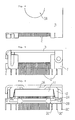
- Figure 1 is a side elevation view showing in exploded fashion a socket according to one embodiment of the present invention, before mounting an electronic package in the socket.
- Figure 2 is a bottom view showing an adapter of the socket of the embodiment of Figure 1.
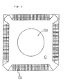
- Figure 3 is a plan view showing a housing member of the socket of Figure 1.
- Figure 4 is a partial view showing the cover of the socket with an electronic package mounted therein.
- Figures 5 and 6 are, respectively, a front view and a vertical sectional view, showing an electronic package mounted in the socket of the preferred embodiment.
- Figure 1 shows an overall view of a socket according to a preferred form of the present invention.
- the reference numeral 1 denotes a housing member having a recess 1A for receiving an electronic package 10.
- Numeral 2 denotes a contact member for making contact with terminals, leads, electrodes 10A or the like of the electronic package mounted in the housing member.
- Numeral 3 denotes a cover for covering the electronic package in the housing member while holding the package under pressure.
- the electronic package comprises an electronic element 11 such as an IC, and an adapter 12 for covering side edges of the electronic element.
- Figure 2 shows a bottom view of the adapter.
- the adapter 12 has slits 12A for aligning the leads of the IC in order, and an opening 12B which will be described later.
- Figure 3 shows the housing member of the socket according to the preferred embodiment.
- grooves 1B are provided to arrange therein the contact members 2 in order.
- One end portion of each of the contact members in the grooves is exposed at a bottom of the recess 1A of the housing member (see Figures 1, 5 and 6) and the other portion of the contact member extends out of the housing member.
- Figures 4 to 6 show the socket in which the electronic package is mounted.
- the cover 3 is made of material having good thermal conductivity, such as aluminum, and has a portion 3A recessed or protruding inwardly for making a face contact with the electronic package.
- the portion 3A is inserted through the opening 12B of the adapter 12, as described, to make contact with a surface of the electronic element mounted in the housing member.
- one side edge of the cover 3 is pivotally mounted on a sidewall of the housing member defining the recess.
- the other side edge of the cover and a sidewall of the housing member opposed to the side edge of the cover comprise latches (3B, 1C) for latching the cover with the housing member.
- the contact member 2 comprises a spring contact 2A for making contact with the terminal or lead of the electronic package, a locking portion 2B for locking to a part of a bottom portion of the housing, and a terminal 2C extending downward out of the housing member (see Figure 6).
- a spring contact 2A for making contact with the terminal or lead of the electronic package
- a locking portion 2B for locking to a part of a bottom portion of the housing
- a terminal 2C extending downward out of the housing member (see Figure 6).
- an end portion of the spring contact is bent obliquely upward.
- the terminals are of three different types. The three types of terminals are different from each other in position on the bottom of the housing member from which the terminals extend downwardly.
- the leads of the element are first received in the adapter in order, and then the adapter holding the element therein is mounted in the housing member. Finally, the housing member receiving the adapter therein is covered by the cover and at the same time the cover and the housing member are latched by the latching means. At such time, the portion of the cover recessed or protruding inwardly is inserted through the opening of the adapter to make contact with the surface of the electronic element mounted in the housing member. Since the portion of the cover is made of material having good thermal conductivity, such as aluminum, heat generated by the electronic element is released through the cover.
- the socket according to the present invention can not only effectively hold therein the leads of the electronic element in order, but can also effectively release the heat generated by the electronic element.
Landscapes
- Engineering & Computer Science (AREA)
- Microelectronics & Electronic Packaging (AREA)
- Connecting Device With Holders (AREA)
- Cooling Or The Like Of Electrical Apparatus (AREA)
Applications Claiming Priority (2)
| Application Number | Priority Date | Filing Date | Title |
|---|---|---|---|
| JP1989141661U JPH0380987U (de) | 1989-12-08 | 1989-12-08 | |
| JP141661/89 | 1989-12-08 |
Publications (3)
| Publication Number | Publication Date |
|---|---|
| EP0431947A2 true EP0431947A2 (de) | 1991-06-12 |
| EP0431947A3 EP0431947A3 (en) | 1991-10-23 |
| EP0431947B1 EP0431947B1 (de) | 1995-05-10 |
Family
ID=15297235
Family Applications (1)
| Application Number | Title | Priority Date | Filing Date |
|---|---|---|---|
| EP90313279A Expired - Lifetime EP0431947B1 (de) | 1989-12-08 | 1990-12-06 | Fassung für einen elektronischen Baustein |
Country Status (5)
| Country | Link |
|---|---|
| US (1) | US5100333A (de) |
| EP (1) | EP0431947B1 (de) |
| JP (1) | JPH0380987U (de) |
| CA (1) | CA2031456A1 (de) |
| DE (1) | DE69019316D1 (de) |
Cited By (2)
| Publication number | Priority date | Publication date | Assignee | Title |
|---|---|---|---|---|
| WO1999018444A1 (en) * | 1997-10-02 | 1999-04-15 | Wells Electronics, Inc. | Test socket for electronic module |
| CN1106690C (zh) * | 1996-10-04 | 2003-04-23 | Lg半导体株式会社 | 半导体封装及其插座 |
Families Citing this family (8)
| Publication number | Priority date | Publication date | Assignee | Title |
|---|---|---|---|---|
| US5216583A (en) * | 1990-07-18 | 1993-06-01 | Kel Corporation | Device for mounting a flat package on a circuit board |
| EP0567255B1 (de) * | 1992-04-24 | 1999-01-20 | Altera Corporation | Oberflächenmontierte Chipträger |
| WO1994028697A1 (en) * | 1993-05-20 | 1994-12-08 | Advanced Interconnections Corporation | Intercoupling component for installing integrated circuit packages on circuit boards |
| US5344334A (en) * | 1993-06-11 | 1994-09-06 | The Whitaker Corporation | Hinged cover for an electrical socket |
| US5801929A (en) * | 1996-11-05 | 1998-09-01 | Cheng; Kan | Clip-on IC retaining apparatus |
| JP2002093541A (ja) * | 2000-09-19 | 2002-03-29 | Miyazaki Oki Electric Co Ltd | Icソケット |
| TW537511U (en) * | 2002-07-26 | 2003-06-11 | Hon Hai Prec Ind Co Ltd | An electronic connector device |
| TWM429683U (en) * | 2012-01-06 | 2012-05-21 | Bothhand Entpr Inc | Packaging case of electronic device |
Family Cites Families (13)
| Publication number | Priority date | Publication date | Assignee | Title |
|---|---|---|---|---|
| US3656183A (en) * | 1970-02-03 | 1972-04-11 | Acs Ind Inc | Connector assembly |
| US4026412A (en) * | 1974-09-26 | 1977-05-31 | Henson Richard D | Electronic circuit carrier and test fixture |
| US3904262A (en) * | 1974-09-27 | 1975-09-09 | John M Cutchaw | Connector for leadless integrated circuit packages |
| US4433886A (en) * | 1981-12-17 | 1984-02-28 | Elco Corporation | Connector mounting for integrated circuit chip packages |
| US4460223A (en) * | 1981-12-30 | 1984-07-17 | Methode Electronics, Inc. | Cover for chip carrier socket |
| JPS59135699U (ja) * | 1983-02-28 | 1984-09-10 | 山一電機工業株式会社 | Icソケツトにおけるic押え装置 |
| US4560217A (en) * | 1983-08-17 | 1985-12-24 | Thomas & Betts Corporation | Chip carrier connector |
| JPS6317550A (ja) * | 1986-07-10 | 1988-01-25 | Yamaichi Electric Mfg Co Ltd | Ic載接形ソケツト |
| US4713022A (en) * | 1986-08-05 | 1987-12-15 | Pfaff Wayne | Socket for flat pack electronic device packages |
| US4824392A (en) * | 1987-11-10 | 1989-04-25 | Amp Incorporated | Burn-in socket for gull wing integrated circuit package |
| GB2214491A (en) * | 1988-01-21 | 1989-09-06 | Dowty Electronic Components | Semiconductor product carriers |
| JP2581817B2 (ja) * | 1988-05-06 | 1997-02-12 | アンプ インコーポレーテッド | チップキャリア用ソケット |
| US5007825A (en) * | 1990-05-21 | 1991-04-16 | Williams Robert M | Heat reclamation apparatus |
-
1989
- 1989-12-08 JP JP1989141661U patent/JPH0380987U/ja active Pending
-
1990
- 1990-11-30 US US07/621,187 patent/US5100333A/en not_active Expired - Lifetime
- 1990-12-04 CA CA002031456A patent/CA2031456A1/en not_active Abandoned
- 1990-12-06 EP EP90313279A patent/EP0431947B1/de not_active Expired - Lifetime
- 1990-12-06 DE DE69019316T patent/DE69019316D1/de not_active Expired - Lifetime
Cited By (2)
| Publication number | Priority date | Publication date | Assignee | Title |
|---|---|---|---|---|
| CN1106690C (zh) * | 1996-10-04 | 2003-04-23 | Lg半导体株式会社 | 半导体封装及其插座 |
| WO1999018444A1 (en) * | 1997-10-02 | 1999-04-15 | Wells Electronics, Inc. | Test socket for electronic module |
Also Published As
| Publication number | Publication date |
|---|---|
| EP0431947B1 (de) | 1995-05-10 |
| CA2031456A1 (en) | 1991-06-09 |
| DE69019316D1 (de) | 1995-06-14 |
| US5100333A (en) | 1992-03-31 |
| EP0431947A3 (en) | 1991-10-23 |
| JPH0380987U (de) | 1991-08-19 |
Similar Documents
| Publication | Publication Date | Title |
|---|---|---|
| US4716494A (en) | Retention system for removable heat sink | |
| US5533908A (en) | Latch and mounting member for a surface mounted electrical connector | |
| US4264114A (en) | Electrical connector assembly | |
| US8215995B1 (en) | Connector attached to a bracket and mounted in a cutout in a substrate | |
| US6181564B1 (en) | IC card | |
| US20080291622A1 (en) | Electrical connector assembly having heat sink | |
| US5100333A (en) | Electronic package socket | |
| US6164998A (en) | Electrical connector having a latching device | |
| US20080064230A1 (en) | Land grid array connector with latch portion | |
| JP2550437B2 (ja) | チップキャリア用ソケット | |
| US20020111052A1 (en) | Low-profile receptacle connector | |
| EP0458525A2 (de) | Elektrischer Steckverbinder hoher Dichte für gedruckte Schaltungen | |
| US6247967B1 (en) | Shielded electrical connector for IC card | |
| US3902777A (en) | Electrical connector assembly | |
| EP1453143B1 (de) | Elektrischer Verbinder mit Erdung | |
| US5022869A (en) | Adapter for use with a bumperless chip carrier | |
| US6293825B1 (en) | Electrical connector | |
| US7207822B2 (en) | Land grid array socket and method for assembling the same | |
| JP3324995B2 (ja) | 電気コネクタ | |
| EP0528228A1 (de) | Chipträgersockelanordnung | |
| US7351087B2 (en) | Land grid array package socket | |
| US7247041B2 (en) | Land grid array connector | |
| US7811095B2 (en) | Socket having aligning keys for accommodating different sizes of integrated chips | |
| KR100280991B1 (ko) | 전기 커넥터의 제조 방법 | |
| EP0856921A2 (de) | Elektrischer Leiterplatten - Steckverbinder mit Halteteilen |
Legal Events
| Date | Code | Title | Description |
|---|---|---|---|
| PUAI | Public reference made under article 153(3) epc to a published international application that has entered the european phase |
Free format text: ORIGINAL CODE: 0009012 |
|
| AK | Designated contracting states |
Kind code of ref document: A2 Designated state(s): BE CH DE ES FR GB IT LI LU NL SE |
|
| PUAL | Search report despatched |
Free format text: ORIGINAL CODE: 0009013 |
|
| AK | Designated contracting states |
Kind code of ref document: A3 Designated state(s): BE CH DE ES FR GB IT LI LU NL SE |
|
| 17P | Request for examination filed |
Effective date: 19920422 |
|
| 17Q | First examination report despatched |
Effective date: 19930608 |
|
| RAP3 | Party data changed (applicant data changed or rights of an application transferred) |
Owner name: THOMAS & BETTS CORPORATION |
|
| GRAA | (expected) grant |
Free format text: ORIGINAL CODE: 0009210 |
|
| AK | Designated contracting states |
Kind code of ref document: B1 Designated state(s): BE CH DE ES FR GB IT LI LU NL SE |
|
| PG25 | Lapsed in a contracting state [announced via postgrant information from national office to epo] |
Ref country code: CH Effective date: 19950510 Ref country code: BE Effective date: 19950510 Ref country code: LI Effective date: 19950510 Ref country code: FR Effective date: 19950510 Ref country code: NL Free format text: LAPSE BECAUSE OF NON-PAYMENT OF DUE FEES Effective date: 19950510 Ref country code: IT Free format text: LAPSE BECAUSE OF FAILURE TO SUBMIT A TRANSLATION OF THE DESCRIPTION OR TO PAY THE FEE WITHIN THE PRESCRIBED TIME-LIMIT;WARNING: LAPSES OF ITALIAN PATENTS WITH EFFECTIVE DATE BEFORE 2007 MAY HAVE OCCURRED AT ANY TIME BEFORE 2007. THE CORRECT EFFECTIVE DATE MAY BE DIFFERENT FROM THE ONE RECORDED. Effective date: 19950510 |
|
| REF | Corresponds to: |
Ref document number: 69019316 Country of ref document: DE Date of ref document: 19950614 |
|
| PG25 | Lapsed in a contracting state [announced via postgrant information from national office to epo] |
Ref country code: SE Effective date: 19950810 |
|
| PG25 | Lapsed in a contracting state [announced via postgrant information from national office to epo] |
Ref country code: DE Effective date: 19950811 |
|
| REG | Reference to a national code |
Ref country code: CH Ref legal event code: PL |
|
| PG25 | Lapsed in a contracting state [announced via postgrant information from national office to epo] |
Ref country code: ES Free format text: LAPSE BECAUSE OF FAILURE TO SUBMIT A TRANSLATION OF THE DESCRIPTION OR TO PAY THE FEE WITHIN THE PRESCRIBED TIME-LIMIT Effective date: 19950821 |
|
| EN | Fr: translation not filed | ||
| NLV1 | Nl: lapsed or annulled due to failure to fulfill the requirements of art. 29p and 29m of the patents act | ||
| PLBE | No opposition filed within time limit |
Free format text: ORIGINAL CODE: 0009261 |
|
| STAA | Information on the status of an ep patent application or granted ep patent |
Free format text: STATUS: NO OPPOSITION FILED WITHIN TIME LIMIT |
|
| 26N | No opposition filed | ||
| PGFP | Annual fee paid to national office [announced via postgrant information from national office to epo] |
Ref country code: ES Payment date: 19961216 Year of fee payment: 7 |
|
| REG | Reference to a national code |
Ref country code: GB Ref legal event code: IF02 |
|
| PGFP | Annual fee paid to national office [announced via postgrant information from national office to epo] |
Ref country code: LU Payment date: 20041001 Year of fee payment: 15 |
|
| PG25 | Lapsed in a contracting state [announced via postgrant information from national office to epo] |
Ref country code: LU Free format text: LAPSE BECAUSE OF NON-PAYMENT OF DUE FEES Effective date: 20051231 |
|
| PGFP | Annual fee paid to national office [announced via postgrant information from national office to epo] |
Ref country code: GB Payment date: 20081229 Year of fee payment: 19 |
|
| GBPC | Gb: european patent ceased through non-payment of renewal fee |
Effective date: 20091206 |
|
| PG25 | Lapsed in a contracting state [announced via postgrant information from national office to epo] |
Ref country code: GB Free format text: LAPSE BECAUSE OF NON-PAYMENT OF DUE FEES Effective date: 20091206 |