EP0433721A2 - Procédé de dépôt d'un revêtement antisoudure sur des plaques de circuit - Google Patents
Procédé de dépôt d'un revêtement antisoudure sur des plaques de circuit Download PDFInfo
- Publication number
- EP0433721A2 EP0433721A2 EP90122756A EP90122756A EP0433721A2 EP 0433721 A2 EP0433721 A2 EP 0433721A2 EP 90122756 A EP90122756 A EP 90122756A EP 90122756 A EP90122756 A EP 90122756A EP 0433721 A2 EP0433721 A2 EP 0433721A2
- Authority
- EP
- European Patent Office
- Prior art keywords
- solder
- mask
- holes
- light
- printed circuit
- Prior art date
- Legal status (The legal status is an assumption and is not a legal conclusion. Google has not performed a legal analysis and makes no representation as to the accuracy of the status listed.)
- Withdrawn
Links
- 229910000679 solder Inorganic materials 0.000 title claims abstract description 95
- 238000000034 method Methods 0.000 title claims abstract description 46
- 239000011248 coating agent Substances 0.000 title 1
- 238000000576 coating method Methods 0.000 title 1
- 229920002120 photoresistant polymer Polymers 0.000 claims abstract description 20
- 229910052709 silver Inorganic materials 0.000 claims abstract description 17
- 239000004332 silver Substances 0.000 claims abstract description 17
- -1 silver halide Chemical class 0.000 claims abstract description 12
- 239000000463 material Substances 0.000 claims abstract description 10
- 230000035945 sensitivity Effects 0.000 claims description 10
- 238000001228 spectrum Methods 0.000 claims description 8
- 238000004519 manufacturing process Methods 0.000 claims description 7
- 108010010803 Gelatin Proteins 0.000 claims description 6
- 229920000159 gelatin Polymers 0.000 claims description 6
- 239000008273 gelatin Substances 0.000 claims description 6
- 235000019322 gelatine Nutrition 0.000 claims description 6
- 235000011852 gelatine desserts Nutrition 0.000 claims description 6
- 230000005855 radiation Effects 0.000 claims description 6
- 239000000758 substrate Substances 0.000 claims description 5
- 239000011230 binding agent Substances 0.000 claims description 3
- 238000005406 washing Methods 0.000 claims description 2
- 150000004820 halides Chemical class 0.000 claims 1
- 230000000873 masking effect Effects 0.000 abstract description 3
- BQCADISMDOOEFD-UHFFFAOYSA-N Silver Chemical compound [Ag] BQCADISMDOOEFD-UHFFFAOYSA-N 0.000 description 6
- 239000004020 conductor Substances 0.000 description 6
- 239000000243 solution Substances 0.000 description 5
- 238000007598 dipping method Methods 0.000 description 4
- 239000003638 chemical reducing agent Substances 0.000 description 3
- 238000005476 soldering Methods 0.000 description 3
- QIGBRXMKCJKVMJ-UHFFFAOYSA-N Hydroquinone Chemical compound OC1=CC=C(O)C=C1 QIGBRXMKCJKVMJ-UHFFFAOYSA-N 0.000 description 2
- YCIMNLLNPGFGHC-UHFFFAOYSA-N catechol Chemical compound OC1=CC=CC=C1O YCIMNLLNPGFGHC-UHFFFAOYSA-N 0.000 description 2
- 238000007590 electrostatic spraying Methods 0.000 description 2
- 150000002500 ions Chemical class 0.000 description 2
- 230000003647 oxidation Effects 0.000 description 2
- 238000007254 oxidation reaction Methods 0.000 description 2
- 238000005507 spraying Methods 0.000 description 2
- 229910001174 tin-lead alloy Inorganic materials 0.000 description 2
- JKFYKCYQEWQPTM-UHFFFAOYSA-N 2-azaniumyl-2-(4-fluorophenyl)acetate Chemical compound OC(=O)C(N)C1=CC=C(F)C=C1 JKFYKCYQEWQPTM-UHFFFAOYSA-N 0.000 description 1
- GRYLNZFGIOXLOG-UHFFFAOYSA-N Nitric acid Chemical compound O[N+]([O-])=O GRYLNZFGIOXLOG-UHFFFAOYSA-N 0.000 description 1
- 239000004697 Polyetherimide Substances 0.000 description 1
- 229910021607 Silver chloride Inorganic materials 0.000 description 1
- 229910021612 Silver iodide Inorganic materials 0.000 description 1
- ATJFFYVFTNAWJD-UHFFFAOYSA-N Tin Chemical group [Sn] ATJFFYVFTNAWJD-UHFFFAOYSA-N 0.000 description 1
- 239000007864 aqueous solution Substances 0.000 description 1
- 238000003287 bathing Methods 0.000 description 1
- 238000004132 cross linking Methods 0.000 description 1
- 230000008021 deposition Effects 0.000 description 1
- 238000010586 diagram Methods 0.000 description 1
- 150000004985 diamines Chemical class 0.000 description 1
- 239000000839 emulsion Substances 0.000 description 1
- 238000005530 etching Methods 0.000 description 1
- 239000011521 glass Substances 0.000 description 1
- 239000004922 lacquer Substances 0.000 description 1
- 229910017604 nitric acid Inorganic materials 0.000 description 1
- 239000003973 paint Substances 0.000 description 1
- 238000000059 patterning Methods 0.000 description 1
- 229920001601 polyetherimide Polymers 0.000 description 1
- ADZWSOLPGZMUMY-UHFFFAOYSA-M silver bromide Chemical compound [Ag]Br ADZWSOLPGZMUMY-UHFFFAOYSA-M 0.000 description 1
- 229940045105 silver iodide Drugs 0.000 description 1
- HKZLPVFGJNLROG-UHFFFAOYSA-M silver monochloride Chemical compound [Cl-].[Ag+] HKZLPVFGJNLROG-UHFFFAOYSA-M 0.000 description 1
- 229910052979 sodium sulfide Inorganic materials 0.000 description 1
- GRVFOGOEDUUMBP-UHFFFAOYSA-N sodium sulfide (anhydrous) Chemical compound [Na+].[Na+].[S-2] GRVFOGOEDUUMBP-UHFFFAOYSA-N 0.000 description 1
- AKHNMLFCWUSKQB-UHFFFAOYSA-L sodium thiosulfate Chemical compound [Na+].[Na+].[O-]S([O-])(=O)=S AKHNMLFCWUSKQB-UHFFFAOYSA-L 0.000 description 1
- 235000019345 sodium thiosulphate Nutrition 0.000 description 1
- 230000003595 spectral effect Effects 0.000 description 1
- 238000002211 ultraviolet spectrum Methods 0.000 description 1
Images

Classifications
-
- H—ELECTRICITY
- H05—ELECTRIC TECHNIQUES NOT OTHERWISE PROVIDED FOR
- H05K—PRINTED CIRCUITS; CASINGS OR CONSTRUCTIONAL DETAILS OF ELECTRIC APPARATUS; MANUFACTURE OF ASSEMBLAGES OF ELECTRICAL COMPONENTS
- H05K3/00—Apparatus or processes for manufacturing printed circuits
- H05K3/22—Secondary treatment of printed circuits
- H05K3/28—Applying non-metallic protective coatings
-
- H—ELECTRICITY
- H05—ELECTRIC TECHNIQUES NOT OTHERWISE PROVIDED FOR
- H05K—PRINTED CIRCUITS; CASINGS OR CONSTRUCTIONAL DETAILS OF ELECTRIC APPARATUS; MANUFACTURE OF ASSEMBLAGES OF ELECTRICAL COMPONENTS
- H05K3/00—Apparatus or processes for manufacturing printed circuits
- H05K3/0073—Masks not provided for in groups H05K3/02 - H05K3/46, e.g. for photomechanical production of patterned surfaces
- H05K3/0082—Masks not provided for in groups H05K3/02 - H05K3/46, e.g. for photomechanical production of patterned surfaces characterised by the exposure method of radiation-sensitive masks
-
- H—ELECTRICITY
- H05—ELECTRIC TECHNIQUES NOT OTHERWISE PROVIDED FOR
- H05K—PRINTED CIRCUITS; CASINGS OR CONSTRUCTIONAL DETAILS OF ELECTRIC APPARATUS; MANUFACTURE OF ASSEMBLAGES OF ELECTRICAL COMPONENTS
- H05K2201/00—Indexing scheme relating to printed circuits covered by H05K1/00
- H05K2201/09—Shape and layout
- H05K2201/09009—Substrate related
- H05K2201/09118—Moulded substrate
-
- H—ELECTRICITY
- H05—ELECTRIC TECHNIQUES NOT OTHERWISE PROVIDED FOR
- H05K—PRINTED CIRCUITS; CASINGS OR CONSTRUCTIONAL DETAILS OF ELECTRIC APPARATUS; MANUFACTURE OF ASSEMBLAGES OF ELECTRICAL COMPONENTS
- H05K2203/00—Indexing scheme relating to apparatus or processes for manufacturing printed circuits covered by H05K3/00
- H05K2203/05—Patterning and lithography; Masks; Details of resist
- H05K2203/0502—Patterning and lithography
- H05K2203/0505—Double exposure of the same photosensitive layer
-
- H—ELECTRICITY
- H05—ELECTRIC TECHNIQUES NOT OTHERWISE PROVIDED FOR
- H05K—PRINTED CIRCUITS; CASINGS OR CONSTRUCTIONAL DETAILS OF ELECTRIC APPARATUS; MANUFACTURE OF ASSEMBLAGES OF ELECTRICAL COMPONENTS
- H05K2203/00—Indexing scheme relating to apparatus or processes for manufacturing printed circuits covered by H05K3/00
- H05K2203/05—Patterning and lithography; Masks; Details of resist
- H05K2203/0548—Masks
- H05K2203/0551—Exposure mask directly printed on the PCB
-
- H—ELECTRICITY
- H05—ELECTRIC TECHNIQUES NOT OTHERWISE PROVIDED FOR
- H05K—PRINTED CIRCUITS; CASINGS OR CONSTRUCTIONAL DETAILS OF ELECTRIC APPARATUS; MANUFACTURE OF ASSEMBLAGES OF ELECTRICAL COMPONENTS
- H05K2203/00—Indexing scheme relating to apparatus or processes for manufacturing printed circuits covered by H05K3/00
- H05K2203/10—Using electric, magnetic and electromagnetic fields; Using laser light
- H05K2203/107—Using laser light
Definitions
- the invention relates to a method for applying a solder stop cover to the circuit pattern of printed circuit boards, in particular of three-dimensional printed circuit boards, with the release of plated-through holes and / or solder pads.
- solder stop cover In the production of printed circuit boards, a solder stop cover should be applied to the areas of the printed circuit board that are not to be soldered after the patterning of the printed circuit board. This solder stop cover only leaves vias and / or solder pads free, so that a solderable end surface can then be produced there by hot tinning or by a remelting process.
- the solder stop cover can be applied by selectively applying a solder mask to the areas to be protected or by applying a light-sensitive solder mask over the entire area, followed by photo structuring. The selective application is associated with too much effort, while the photo structuring, particularly in the case of three-dimensional circuit boards, cannot be carried out using conventional masking techniques.
- the invention has for its object to provide an economical method for applying a solder stop cover on circuit boards, which is also applicable to three-dimensional circuit boards.
- a mask is thus applied to the solder resist, with the aid of which the photo-structuring of the solder resist can be carried out in a simple manner even with three-dimensional circuit boards.
- Proven techniques can be used in the production of this mask, which can also be carried out without problems with three-dimensional circuit boards.
- a light-sensitive layer of a photographic material based on silver halide is applied to the entire surface of the solder mask to produce the mask and selectively exposed and developed in the area of the plated-through holes and / or solder pads, whereupon the unexposed areas of the light-sensitive layer are removed or can be fixed by washing out the unexposed silver halide.
- the silver ions are reduced to silver by the selective exposure and development of the photographic material in the area of the plated-through holes and / or soldering pads, so that after removal of the non-reduced silver halide when fixing, an exact mask of silver remains, with the aid of which Photo structuring of the solder mask is carried out. It should be emphasized in particular that the critical blackening of the photographic material by exposure and development or reduction is possible even in the critical inner region of the plated-through holes due to the extremely high sensitivity to light of the silver halides.
- a negative-working photoresist is applied to the entire surface of the solder resist and in the area of vias and / or to produce the mask Solder pads are selectively exposed and developed.
- the disadvantages of photo-structuring photosensitive solder resists are thus avoided by using a conventional negative-working photo resist.
- a light-sensitive layer is used, the sensitivity spectrum of which lies at longer wavelengths than the sensitivity spectrum of the solder resist underneath.
- the selective exposure of the light-sensitive layer in the area of the plated-through holes and / or solder pads is preferably carried out with the aid of a laser, in particular an Ar laser.
- the laser beams can in particular be directed specifically into the via holes and there ensure perfect exposure of the photographic material.
- the exposed areas of the light-sensitive layer are removed by dissolving the gelatin used as a binder.
- Such solution processes for removing the mask consisting of silver can be carried out particularly economically.
- a negative-working photoresist is used, the sensitivity spectrum of which lies at longer wavelengths than the sensitivity spectrum of the solder resist underneath.
- an undesired exposure of the solder resist during the production of the mask can be excluded with certainty.
- the selective exposure of the negatively working photoresist in the area of the plated-through holes and / or solder pads is then preferably also carried out in this case with the aid of a Lasers, especially with the help of an Ar laser.
- the laser beams can again be directed specifically into the via holes and there ensure perfect exposure of the negatively working photoresist.
- the movement of the laser beam relative to the circuit board should preferably be freely programmable, i.e. the description and exposure of vias and / or solder pads can then be carried out in a particularly simple manner.
- the exposure of the solder resist in step c) is carried out by floodlights.
- Such exposure using escape light requires particularly little effort.
- UV radiation has proven itself as an escape light, which enables the conventional photostructurable solder resist to be properly exposed.
- FIG. 1 shows a section through a part of a printed circuit board, on the electrically insulating substrate 1 of which conductor tracks 2, through contacts 3 and solder pads 4 have been applied as a conductor pattern.
- the substrate 1 shown is an injection-molded base material with injected holes for the plated-through holes 3.
- Glass fiber-reinforced polyetherimide, for example, is suitable as the material for such a substrate 1.
- solder stop cover To apply a solder stop cover to the conductor pattern of the conductive plate shown in detail in FIG. 1, leaving through contacts 3 and solder pads 4, a light-sensitive solder resist 5 is now applied over the whole area according to FIG. 2 by dipping or by electrostatic spraying.
- a suitable solder mask 5 is sold, for example, by Peters D-4152 Kempen under the trade name ELPEMER ES 2469 SM.
- the spectral sensitivity of this solder resist is in the wavelength range from 350 to 400 nm.
- a light-sensitive layer 6 of a photographic material based on silver halide is applied over the whole area according to FIG. 3 by dipping or spraying.
- This photographic material is a photographic silver halide emulsion with silver chloride and / or silver bromide and / or silver iodide grains in gelatin.
- the light-sensitive layer 6 is then exposed in the area of the plated-through holes 3 and the soldering pads 4 with the aid of a laser in a scanning process, the laser radiation being merely indicated by arrows Ls.
- the arrows in the inner region of the plated-through hole are intended to show that the exposure of the layer 6 in the region of the hole wall can be improved by an oblique incidence of the laser beams Ls.
- frequency-doubled Nd: YAG lasers or preferably Ar ion lasers can be used to generate the laser beams Ls. With such lasers it is reliably excluded that the UV-sensitive solder resist 5 underneath is also exposed.
- the latent image generated in the exposure according to FIG. 4 in the light-sensitive layer 6 in the area of the through-contacts 3 and solder pads 4 is made visible by developers in the form of a blackening.
- the exposed and developed areas 600 of the photosensitive layer 6 are also highlighted in FIG. 4 by a blackening.
- Suitable developers consist essentially of alkaline aqueous solutions of a reducing agent, suitable as reducing agents being, for example, hydroquinone, catechol and generally aromatic amino alcohols or diamines. Addition of sodium sulfide reduces the air oxidation of the dissolved reducing agents and intercepts oxidation products formed during development.
- the unexposed areas of the photosensitive layer 6 are made light-resistant.
- fixing the non-reduced silver halide is washed out, for example, by bathing in a sodium thiosulfate solution, so that a gelatin layer 60 which is transparent to light remains here.
- the exposed areas 600 which are opaque to light are then a metallic mask consisting essentially of silver.
- this mask shields the areas below. UV radiation is preferably used as the floodlight F.
- the exposed areas 600 of the photosensitive layer 6 are removed.
- the silver is dissolved in a suitable etching solution, for example in nitric acid.
- a suitable etching solution for example in nitric acid.
- the gelatin layer 60 is then simultaneously dissolved. While the exposed areas of the solder mask 5 are identified in FIG. 6 by the reference number 50, the unexposed areas of the solder mask 5 exposed by the removal of the mask 600 are provided with the reference number 500.
- the unexposed areas 500 of the solder mask 5 are developed by immersing the entire printed circuit board in a commercially available developer solution and thereby completely removed. According to FIG. 7, only the exposed areas 50 of the solder mask remain 5, which, with the exception of the plated-through holes 3 and the solder pads 4, completely cover all areas of the printed circuit board and in particular the conductor tracks 2. Subsequent hot tinning enables the plated-through holes 3 and the solder pads to be selectively coated with a tin-lead alloy without any problems.
- solder stop cover To apply a solder stop cover to the circuit diagram of the circuit board shown in detail in FIG. 8, leaving through-holes 3 and solder pads 4 exposed, a light-sensitive solder resist 5 is first applied over the whole area according to FIG. 9 by dipping or by electrostatic spraying. This solder resist 5 is again the negative paint used in the first embodiment.
- a negative-working photoresist 6a is applied over the whole area according to FIG. 10 by dipping, spraying or the like.
- This photoresist 6a is a commercially available product which becomes poorly soluble or insoluble through crosslinking or photopolymerization.
- Such negative working photoresists are used, for example, in the manufacture of printed circuit boards.
- a negative-working photoresist is suitable, which can be exposed outside the UV spectrum with an Ar laser at wavelengths of 488 nm.
- the negatively working photoresist 6a is then exposed in the area of the plated-through holes 3 and the soldering pads 4 with the aid of a laser in a scanning process, the laser radiation being merely indicated by arrows Ls.
- the arrows in the interior of the via are intended to show that the exposure of the photoresist 6a in the region of the hole wall can be improved by an oblique incidence of the laser beams Ls.
- Ar ion lasers for example, can be used to generate the laser beams Ls. With such lasers it is excluded with certainty that the UV-sensitive solder resist 5 underneath is also exposed.
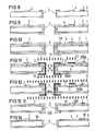
- the exposed areas of the photoresist 6a form a mask which is highlighted by a blackening in FIG. 11 and is identified by the reference number 600a.
- Fig. 12 also shows that the mask 600 a shields the areas below when the solder resist 5 is exposed to floodlight F. Again, UV radiation is preferably used as the floodlight F here.
- the mask 600 a After the selective exposure of the solder resist 5 described above, according to FiG. 13 the mask 600 a removed.
- the mask 600a corresponding to the exposed areas of the photoresist 6a is removed in a commercially available stripper.
- the unexposed areas 500 of the solder mask 5 are developed by immersion in a developer solution and thereby completely removed.
- solderable end surface in the area of the plated-through holes 3 and solder pads 4 can then also be produced in this case by hot tinning or by a remelting process.
Landscapes
- Engineering & Computer Science (AREA)
- Manufacturing & Machinery (AREA)
- Microelectronics & Electronic Packaging (AREA)
- Non-Metallic Protective Coatings For Printed Circuits (AREA)
- Photosensitive Polymer And Photoresist Processing (AREA)
- Exposure And Positioning Against Photoresist Photosensitive Materials (AREA)
Applications Claiming Priority (2)
| Application Number | Priority Date | Filing Date | Title |
|---|---|---|---|
| DE3942741 | 1989-12-22 | ||
| DE3942741 | 1989-12-22 |
Publications (2)
| Publication Number | Publication Date |
|---|---|
| EP0433721A2 true EP0433721A2 (fr) | 1991-06-26 |
| EP0433721A3 EP0433721A3 (en) | 1992-07-08 |
Family
ID=6396286
Family Applications (1)
| Application Number | Title | Priority Date | Filing Date |
|---|---|---|---|
| EP19900122756 Withdrawn EP0433721A3 (en) | 1989-12-22 | 1990-11-28 | Method of applying a solder stop coating on printed circuit boards |
Country Status (2)
| Country | Link |
|---|---|
| EP (1) | EP0433721A3 (fr) |
| JP (1) | JPH04122091A (fr) |
Cited By (1)
| Publication number | Priority date | Publication date | Assignee | Title |
|---|---|---|---|---|
| CN114340196A (zh) * | 2022-01-11 | 2022-04-12 | 珠海中京电子电路有限公司 | 一种防止阻焊相交孔溢油的方法、pcb板及应用 |
Family Cites Families (8)
| Publication number | Priority date | Publication date | Assignee | Title |
|---|---|---|---|---|
| JPS5497782A (en) * | 1978-01-19 | 1979-08-02 | Nippon Electric Co | Method of forming photoresist film |
| GB2117670B (en) * | 1982-04-06 | 1985-06-26 | Dainippon Ink & Chemicals | Method for forming a cured resin coating having a desired pattern on the surface of a substrate |
| EP0197519A3 (fr) * | 1985-04-10 | 1989-01-11 | International Business Machines Corporation | Procédé pour réaliser des patrons de masquage et de réserve |
| US4666818A (en) * | 1985-06-10 | 1987-05-19 | The Foxboro Company | Method of patterning resist for printed wiring board |
| JPS6381893A (ja) * | 1986-09-25 | 1988-04-12 | キヤノン株式会社 | スルホ−ル導通回路基体の製造方法 |
| GB2202093A (en) * | 1987-03-11 | 1988-09-14 | Marconi Instruments Ltd | Making printed circuit boards |
| JPH01129490A (ja) * | 1987-11-14 | 1989-05-22 | Tanazawa Hatsukoushiya:Kk | プリント基板用レジスト層成形方法 |
| JPH01191494A (ja) * | 1988-01-27 | 1989-08-01 | Toshiba Corp | プリント基板の製造方法 |
-
1990
- 1990-11-28 EP EP19900122756 patent/EP0433721A3/de not_active Withdrawn
- 1990-12-21 JP JP2413536A patent/JPH04122091A/ja active Pending
Cited By (1)
| Publication number | Priority date | Publication date | Assignee | Title |
|---|---|---|---|---|
| CN114340196A (zh) * | 2022-01-11 | 2022-04-12 | 珠海中京电子电路有限公司 | 一种防止阻焊相交孔溢油的方法、pcb板及应用 |
Also Published As
| Publication number | Publication date |
|---|---|
| JPH04122091A (ja) | 1992-04-22 |
| EP0433721A3 (en) | 1992-07-08 |
Similar Documents
| Publication | Publication Date | Title |
|---|---|---|
| DE2420589C3 (de) | Verfahren zum Herstellen von Photolackmustern | |
| DE2460988C2 (de) | Verfahren zum Niederschlagen eines Musters aus einem dünnen Film auf einem anorganischen Substrat | |
| EP0002795B1 (fr) | Procédé pour la fabrication de masques pour les procédés lithographiques utilisant un photorésist | |
| DE3689659T2 (de) | Bildaufzeichnungsverfahren für gedruckte schaltungen. | |
| DE1771076C3 (de) | Verfahren zur Herstellung eines Mosaikschirmes für eine Farbfernsehröhre | |
| DE69306178T2 (de) | Ablatives Verfahren für die Leiterplattentechnologie | |
| DE4417245A1 (de) | Verfahren zur strukturierten Metallisierung der Oberfläche von Substraten | |
| DE2628099A1 (de) | Verfahren zum herstellen einer maske | |
| DE1917474B2 (de) | Verfahren zum Herstellen metallischer Muster auf einer Unterlage | |
| DE3108080A1 (de) | Verfahren zur herstellung einer gedruckten schaltung | |
| DE3729733C2 (fr) | ||
| DE68917918T2 (de) | Kryogenes verfahren für metallabzug. | |
| EP0433720A2 (fr) | ProcédÀ© de dépôt d'un revêtement antisoudure sur des plaques de circuit imprimé | |
| DE2539690A1 (de) | Verfahren zum entwickeln von resistfilmen | |
| EP0433721A2 (fr) | Procédé de dépôt d'un revêtement antisoudure sur des plaques de circuit | |
| DE69010353T2 (de) | Aperturmusterdruckplatte für eine Schattenmaske und Herstellungsverfahren dafür. | |
| EP0127794A2 (fr) | Méthode pour la fabrication de plaquettes à circuit imprimé | |
| DE19857094B4 (de) | Verfahren zum Verringern/zum lokalen Verringern eines Resistmusters in einer Hableitervorrichtung | |
| EP0355194B1 (fr) | Procédé de fabrication de plaques de circuit à trous traversants comportant de très petits oeillets de soudage ou n'en comportant pas autour des trous traversants | |
| JP2794865B2 (ja) | プリント基板の製造方法 | |
| DE2400665B2 (de) | Verfahren zur herstellung eines lotabweisenden schutzes auf leiterplatten mit durchgehenden loechern | |
| DE3324117A1 (de) | Verfahren und herstellung gedruckter schaltungen und photolack zur durchfuehrung dieses verfahrens | |
| DE1109226B (de) | Verfahren zur Herstellung gedruckter Schaltungen und/oder gedruckter Schaltungselemente | |
| DE2003983B2 (de) | Photographisches verfahren zur herstellung elektrischer schaltungen | |
| DE2452326A1 (de) | Verfahren zur herstellung einer aetzmaske mittels energiereicher strahlung |
Legal Events
| Date | Code | Title | Description |
|---|---|---|---|
| PUAI | Public reference made under article 153(3) epc to a published international application that has entered the european phase |
Free format text: ORIGINAL CODE: 0009012 |
|
| 17P | Request for examination filed |
Effective date: 19901220 |
|
| AK | Designated contracting states |
Kind code of ref document: A2 Designated state(s): AT BE CH DE FR GB IT LI NL SE |
|
| PUAL | Search report despatched |
Free format text: ORIGINAL CODE: 0009013 |
|
| AK | Designated contracting states |
Kind code of ref document: A3 Designated state(s): AT BE CH DE FR GB IT LI NL SE |
|
| STAA | Information on the status of an ep patent application or granted ep patent |
Free format text: STATUS: THE APPLICATION IS DEEMED TO BE WITHDRAWN |
|
| 18D | Application deemed to be withdrawn |
Effective date: 19930109 |