EP0434081A2 - Überwachungsgerät zur selektiven Feststellung von einem Signalzustand in einem Betriebssystem - Google Patents
Überwachungsgerät zur selektiven Feststellung von einem Signalzustand in einem Betriebssystem Download PDFInfo
- Publication number
- EP0434081A2 EP0434081A2 EP90125077A EP90125077A EP0434081A2 EP 0434081 A2 EP0434081 A2 EP 0434081A2 EP 90125077 A EP90125077 A EP 90125077A EP 90125077 A EP90125077 A EP 90125077A EP 0434081 A2 EP0434081 A2 EP 0434081A2
- Authority
- EP
- European Patent Office
- Prior art keywords
- trigger
- points
- conditions
- signals
- bus
- Prior art date
- Legal status (The legal status is an assumption and is not a legal conclusion. Google has not performed a legal analysis and makes no representation as to the accuracy of the status listed.)
- Granted
Links
Images


Classifications
-
- G—PHYSICS
- G06—COMPUTING OR CALCULATING; COUNTING
- G06F—ELECTRIC DIGITAL DATA PROCESSING
- G06F11/00—Error detection; Error correction; Monitoring
- G06F11/30—Monitoring
- G06F11/34—Recording or statistical evaluation of computer activity, e.g. of down time, of input/output operation ; Recording or statistical evaluation of user activity, e.g. usability assessment
- G06F11/3466—Performance evaluation by tracing or monitoring
- G06F11/348—Circuit details, i.e. tracer hardware
-
- G—PHYSICS
- G06—COMPUTING OR CALCULATING; COUNTING
- G06F—ELECTRIC DIGITAL DATA PROCESSING
- G06F11/00—Error detection; Error correction; Monitoring
- G06F11/30—Monitoring
- G06F11/34—Recording or statistical evaluation of computer activity, e.g. of down time, of input/output operation ; Recording or statistical evaluation of user activity, e.g. usability assessment
- G06F11/3466—Performance evaluation by tracing or monitoring
- G06F11/349—Performance evaluation by tracing or monitoring for interfaces, buses
-
- G—PHYSICS
- G06—COMPUTING OR CALCULATING; COUNTING
- G06F—ELECTRIC DIGITAL DATA PROCESSING
- G06F11/00—Error detection; Error correction; Monitoring
- G06F11/30—Monitoring
- G06F11/34—Recording or statistical evaluation of computer activity, e.g. of down time, of input/output operation ; Recording or statistical evaluation of user activity, e.g. usability assessment
- G06F11/3466—Performance evaluation by tracing or monitoring
- G06F11/3495—Performance evaluation by tracing or monitoring for systems
Definitions
- the present invention relates to monitoring the operation of computer systems and, more particularly, to apparatus for selectively detecting signal conditions at points in an operating system and for recording said conditions.
- the user of a monitoring apparatus of the prior art generally has the ability to capture all of the events occurring from a single source within a given time after initiation of the monitoring process, but not the ability to selectively capture information related to specific, selected events that might occur independently from several sources and at any time after start of the monitoring. That is, the monitoring apparatus of the prior art operates in much the same manner as a tape recorder, turn it on and it records everything that happen until it runs out of tape.
- the user has difficulty in capturing events that may occur only at infrequent intervals or only long after the monitoring process has started and may not, in fact, capture the events of interest because the monitoring device's data recording apparatus becomes saturated, or filled with data. This is particularly true in the case of events which are either intermittent, such as certain types of failures, or which happen only infrequently in the normal operation of a system.
- the monitoring devices of the prior art are generally not capable of selectively defining and capturing events of interest, but must capture much data which is not of interest in order to capture the data that is of interest, and cannot monitor events from a variety of sources, making repetitive monitoring operations necessary to establish correlations between events at various sources.
- a monitor apparatus comprising a condition sensing circuit coupled to a first set of points in said system for sensing predetermined signal conditions at said first set of points and for generating first-type output signals upon the occurrence of said predetermined conditions, an enabling circuit for storing a plurality of codes corresponding to different ones of said first-type output signals and for delivering second-type output signals representing said codes, and a detecting circuit coupled to said condition sensing circuit and to said enabling circuit and responsive to said first-type and second-type signals for generating third-type output signals upon the occurrence of first-type output signals corresponding to said second-type output signals.
- storage means are coupled to a second set of points in said system and to said detecting circuit, which are responsive to said third-type output signals for recording representations of the signal conditions present at said second set of points.
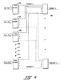
- System 10 includes at least one Central System 14, which performs information processing operations, and a Memory 16 for storing programs and data.
- CSS 14 Central System 14
- Memory 16 and other elements of the system, such as other Central Systems and memories, and input and output controllers, through a System Bus (SYSBUS).
- System buses such as SYSBUS 18 are well known in the art and an example of such could be the MEGABUS* (*MEGABUS is a trademark of Bull HN Information Systems Inc.) used in Bull HN Information System's DPS6 and MRX computer systems.
- System 10 includes a Private Bus (PBUS) which is connected between Memory 16 and CSS 14 and which is used solely to communicate information, that is, program instructions and data, from Memory 16 to CSS 14.
- PBUS 20 is representative of the special purpose buses often found in computer systems and, in System 10, is provided to enhance the speed with which information may be read from Memory 14 to CSS 12.
- memory write operations are executed completely on SYSBUS 18 in the usual manner and certain memory read operations may be executed entirely through SYSBUS 18 in the usual manner.
- Many memory read operations are of blocks of words, for example, of blocks of eight double words.
- the read command and starting address of the block to be read are provided to Memory 16 through SYSBUS 18, in the usual manner for a read operation, and the block of words is then read from Memory 16 to CSS 14 through PBUS 20 as a burst of eight double words.
- the speed of the block read operation is thereby enhanced by avoiding the more complex and slower protocols used in communicating through general purpose SYSBUS 18.
- CSS 14 has associated with it a Central Processing Unit Bus (CPUBUS) 22 for communication among the elements of CSS 14 and SYSBUS 18 and PBUS 20 communicate with CPUBUS 22 through, respectively, a bidirectional SYSBUS Interface (SBI) 24 and a unidirectional PBUS Interface (PBI) 26.
- CPUBUS Central Processing Unit Bus
- SBI SYSBUS Interface
- PBI unidirectional PBUS Interface
- CSS 14 is in turn comprised of a number of elements, including a Central Process Unit (CPU) 28 which, in the present embodiment of System 10, may be an Intel 80386 microprocessor, which is well known to those of ordinary skill in the art.
- CPUBUS 22 accordingly is a standard 32 bit 80386 bus using the 80 386 data, instruction and command formats and executing the 80386 bus protocols and procedures.
- CPU 28 Associated with CPU 28 are a local Random Access Memory (RAM) 30 for use by CPU 28, such as storing data and instructions, a Read Only Memory (ROM) 32 used, for example, to store system boot programs, and an Erasable Programmable Read Only Memory (EPROM) 34 which is related to Bus Monitor 12 and will be discussed further below.
- RAM Random Access Memory
- ROM Read Only Memory
- EPROM Erasable Programmable Read Only Memory
- CSS 14 includes a number of other CPU 28 related elements, generally referred to as Process and Communication Elements (PCE) 36, which may include such well known functions as interrupt handling logic and communications controllers, such as disk drive controllers and serial and parallel port controllers.
- PCE Process and Communication Elements
- Bus Monitor 12 the function of Bus Monitor 12 is to continuously monitor the conditions present at a first set of selectable monitored points while System 10 is in operation. As will be described, those points include System 10's buses, most particularly SYSBUS 18, and may include Memory 16 and certain other selected points inside or outside System 10.
- Bus Monitor 12 Should Bus Monitor 12 detect any of a number of preselected trigger conditions occurring at one or more of this first set of points, Bus Monitor 12 will generate a trigger output indicating the occurrence of that condition. Such a condition, or a selectable time sequence of such triggers, will cause the sampling and storing of the states then present at a second set of selectable sampled points for subsequent examination.
- the second set of points may include some or all of the first set of points, such as the signals present on SYSBUS 18, and may include further points in System 10, such as PBUS 20.
- Trigger Control 38 has inputs comprising the first set of monitored conditions. As indicated, these Trigger Control 38 inputs are connected from SYSBUS 18, from selectable External Triggers (EXTTRG) 42, and from Illegal/Error Condition Triggers (ILGL/ERR) 44. As will be described, Trigger Control 38 is programmable to detect certain conditions, that is, combinations, patterns or sequences of states or signals occurring in the monitored inputs, and to generate corresponding trigger outputs indicating the detection of one or more of the programmably selected conditions. These triggers may be used directly to initiate the sampling of the conditions then present on the monitored points of System 10, or Trigger Control 38 may also be programmed to generate an output upon a selected time sequential occurrence of triggers.
- EXTTRG selectable External Triggers
- ILGL/ERR Illegal/Error Condition Triggers
- Bus Monitor 12 is programmed through CSS 14 and, as shown, Trigger Control 38 is bidirectional connected to CPUBUS 22 through Bus Monitor Interfaces (BMI) 46. This connection allows CSS 14 to write selected trigger conditions into Trigger Control 38 and to read the state of Trigger Control 38.
- BMI Bus Monitor Interfaces
- Silo Bank 40 comprises the memory for storing, or recording, the sampled conditions present in System 10 when a trigger condition is detected by Trigger Control 38 and accordingly has a sample control input connected from Trigger Control 38.
- the data inputs of Silo Bank 40 are connected from the second set of selected sample points and include, as shown in Fig. 1, the data, command and address lines of SYSBUS 18, the lines of PBUS 20, the set of selectable external points from EXTTRG 42.
- the sample inputs of Silo Bank 40 further include a time stamp generated by Trigger Control 38.
- Silo Bank 40 in turn has data outputs connected to CPUBUS 22, so that the contents of Silo Bank 40 may be read to CSS 14 for examination or transfer to other destinations, such as a remote monitoring facility.
- Bus Monitor 12 has a set of Interrupt/ Pattern Programmable Registers (IPPR) 48 connected from CPUBUS 22 and to SYSBUS 18.
- IPPR 48 is used by CSS 14 to test SYSBUS 18 and system elements connected from SYSBUS 18 by allowing CSS 14 to write test patterns onto SYSBUS 18 through IPPR 48 under the control of CSS 14.
- CSS 14 may write selected commands into IPPR 48, such as a system or CPU interrupt command, and store the command in IPPR 48 until the command is written onto SYSBUS 18 by the occurrence of a trigger output from Trigger Control 38.
- Bus Monitor 12 Having described the overall structure and operation of a System 10 incorporating a Bus Monitor 12 of the present invention, and the general structure and operation of Bus Monitor 12, the following will describe Bus Monitor 12 in further detail.
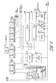
- FIG. 2 therein is shown a more detailed block diagram of Bus Monitor 12, with the exception of IPPR 48.
- Silo Bank 40 Located across the top of Fig. 2 is Silo Bank 40 which, as shown, is comprised of three sub-silos, each corresponding to a point in System 10 whose condition, or state, is to be recorded upon the occurrence of a corresponding trigger output from Trigger Control 38. As shown, these sub-silos comprise a SYSBUS Silo (SSL) 50, a PBUS Silo (PSL) 52, and an External Trigger Silo (XSL) 54. Each of these sub-silos is in turn comprised of three silo segments, each segment being assigned to the recording of a particular set of conditions from the corresponding point in System 10.
- SSL SYSBUS Silo
- PSL PBUS Silo
- XSL External Trigger Silo
- SSL 50 is comprised of a SYSBUS Data Silo (SDSL) 56, a SYSBUS Address Silo (SASL) 58, a SYSBUS Command Silo (SCSL) 60, and a SYSBUS Time Stamp Silo (STSL) 62.
- SDSL SYSBUS Data Silo
- SASL SYSBUS Address Silo
- SCSL SYSBUS Command Silo
- STSL SYSBUS Time Stamp Silo
- PSL 52 is comprised of a PBUS Data Silo (PDSL) 64 and a PBUS Time Stamp Silo (PTSL) 66
- XTSL 54 is comprised of an External Data Silo (XDSL) 68 and an External Time Stamp Silo (XTSL) 70.
- XDSL External Data Silo
- XTSL External Time Stamp Silo
- SDSL 56, SASL 58, SCSL 60 and STSL 62 have data inputs connected from, respectively, the data, address and command lines of SYSBUS 18 and the output of a time stamp generator.
- PDSL 64 and PTSL 66 have data inputs connected from, respectively, the lines of PBUS 20 and the time stamp generator, while XDSL 68 and XTSL 70 have data inputs connected, respectively, from the external sample points, for example, EXTTRG 42, and, again, the time stamp generator.
- the data outputs (DOs) of SSL 50, PSL 52 and XSL 54 are, as shown, connected in parallel to the data inputs of Silo Output Register (SOR) 72 and the data outputs of SOR 72 are connected in turn to CPUBUS 22.
- SOR Silo Output Register
- CSS 14 may address and read the contents of any of SSL 5O, PSL 52 or XSL 54 to CPUBUS 22 through SOR 72.
- SSL 50, PSL 52 and XSL 54 are comprised of video RAMs (Random Access Memories), such as are used in personal computers to store and provide the video display outputs.
- video RAMs Random Access Memories
- video RAMs are comprised of two memory components, the first being a large, relatively slow dynamic memory used to store large volumes of information, such as graphics to be displayed on a display screen, and a smaller and much faster static memory.
- data is written into the dynamic memory portion of a video RAM at a relatively low speed, is subsequently and selectively transferred into static memory portion of the RAM, and read from the static memory portion at a much higher speed, for example, to a graphics display unit.
- Bus Monitor 12 data is read at high speed into the dynamic memory portion of the video RAM, thereby allowing high speed capture of information present on the monitored points of System 10, such as SYSBUS 18 and transferred into the much larger though slower memory comprised of the dynamic memory portion of the video RAM, from which it may be subsequently read at much lower speeds.
- the use of video RAMs for Silo Bank 40 thereby provides a memory unit having high speed write and data capture capabilities, in the static memory portion of the video RAM, combined with the high storage volume and low costs of the dynamic memory portion of the video RAM.
- BMIs 46 Located in the lower left corner of Fig. 2 are BMIs 46 which, as shown, are comprise a SYSBUS BMI (SBMI) 74, a PBUS BMI (PBMI) 76, and an External BMI (XBMI) 78 which provide interfaces between CPUBUS 22 and, respectively, SSL 50, PSL 52 and XSL 54.
- SBMI 74, PBMI 76 and XBMI 78 are essentially identical and each includes an Address and Register Counter (ADRRC) 80 which has data inputs connected from CPUBUS 22 and a clock input connected from the read/write control and timing circuitry for Silo Bank 40.
- ADRRC Address and Register Counter
- the ADRRC 80's generate and provide read and write addresses to Silo Bank 40 and may be loaded with addresses from CSS 14, for example, to select information to be read from Silo Bank 40 and to initialize the starting addresses at which sampled information is written into Silo Bank 40.
- the ADRRC 80 clock inputs from the read/ write timing and control circuitry are primarily used to generate successive addresses for writing sampled information into Silo Bank 40 and reading the recorded information from Silo Bank 40.
- Each of SBMI 74, PBMI 76 and XBMI 78 also includes a Decode Register (DCDR) 82 connected from the outputs of the ADRRC 80 and which decodes the contents of the ADRRC 80s to generate, in the present implementation of Bus Monitor 12, the address and column select inputs to the memory elements of SSL 50, PSL 52 and XSL 54.
- DCDR Decode Register
- each of SBMI 74, PBMI 76 and XBMI 78 also includes a Register Store (RS) 84 having data inputs connected from the outputs of the respective ADRRC 80s and data outputs connected to CPUBUS 22, so that the contents of the ADRRC 80s may be read to CSS 14 through CPUBUS 22.
- RS Register Store
- RSCD Register/Silo Control/Decode
- CNTLTMG Control and Timing
- RSCD 86 is connected from CPUBUS 22 to receive and decode addresses and operations commands from CSS 14, such as the addresses and commands to write an address into a BMI 46 or to read information from an address in one or more of the elements of Silo Bank 40, and to provide the corresponding control outputs to the elements of Bus Monitor 12, including CNTLTMG 88.
- CNTLTMG 88 provides the detailed control and timing signals to the register and memory elements of Bus Monitor 12, in particular the memory elements of SSL 50, PSL 52 and XSL 54.
- CNTLTMG 88 has an input from a Trigger output of the trigger detection logic, described in detail in the following, for the purpose of controlling the writing of data from the selected sample points into SSL 50, PSL 52 and XSL 54, and a time stamp, when, as previously described, Bus Monitor 12 detects a selected trigger condition.
- the design and operation of RSCD 86 and CNTLTMG 88 are conventional and determined at the detailed level by the operations of Bus Monitor 12, which will be described in detail in the following, and the particular circuits chosen for the individual register and memory elements of Bus Monitor 12. As such, and because the design of such as RSCD 86 and CNTLTMG 88 are well known to those of ordinary skill in the art, RSCD 86 and CNTLTMG 88 will not be described in further detail.
- Trigger Control 38 The primary elements comprising Trigger Control 38 are shown in the lower right portion of Fig. 2 and include Trigger Enable Register (TRIGENR) 90, Trigger Memory (TRIGMEM) 92, Illegal/Error Condition Detector (ELGL/ER) 94, Trigger Detector Logic (TRIGDET) 96, Trigger Registers (TRIGREG) 98 and Time Stamp Generator (TSG) 100.
- Trigger Enable Register (TRIGENR) 90
- Trigger Memory TRIGMEM
- ELGL/ER Illegal/Error Condition Detector
- TRIGDET Trigger Detector Logic
- TSG Time Stamp Generator
- the outputs from TRIGMEM 92, ELGL/ER 94 and the inputs from EXTTRG 42 are trigger signals representing the occurrence of conditions being monitored while TRIGENR 90 stores information, in the form of trigger enabling codes, determining what particular monitored conditions will result in a sampling trigger while.
- TRIGDET 96 and TRIGREG 98 compare the triggers representing the occurrence of conditions being monitored with the present and previous trigger condition inputs from TRIGENR 90 and generate a trigger output, TRIGS, when a set of monitored conditions match the criteria stored in TRIGENR 90.
- TRIGENR 90 has data inputs connected from CPUBUS 22 and receives and stores a set of programmably selectable trigger enable control codes, each of which represents a particular monitored condition or combination of monitored conditions which will result in a trigger output from TRIGDET 96 and TRIGREG 98, or a time sequential combination of triggers which will result in such a trigger output.
- a trigger output of TRIGDET 96 and TRIGREG 98 results in the sampling, and storage in the appropriate portion of Silo Bank 40, of the conditions then present on the selected sampling points in System 10.
- the trigger output may also cause an interrupt to be provided to CPU 28, and will determine which of the silo units comprising Silo Bank 40, SSL 50, PSL 52, or XSL 54, is to receive and store information.
- the trigger enable control codes implemented in the present embodiment of TRIGENR 90 include 16 enabling codes that relate directly to 16 corresponding trigger inputs provided to TRIGDET 96 from the monitored points in System 10, and other codes which define, as trigger conditions, certain combinations or sequences of those 16 trigger conditions.
- TRIGENR 90 may also store other enabling codes to cause TRIGDET 96 and TRIGREG 98 to generate other control signals to Bus Monitor 12, such as an output to transfer a command stored in ITPR 48, such as a CSS 14 interrupt command, onto SYSBUS 18.
- TRIGENR 90 may contain up to 32 enabling codes, most of which are concerned with enabling certain triggers and sequence or combinations of triggers.
- the first block of codes are a set of 12 trigger enable codes (ENable TRigger ?), ENTRGA through ENTRGM, for enabling Bus Monitor 12 to respond to, respectively, each of Triggers A through M.
- the first 8 Trigger Enable Codes, ENTRGA through ENTRGH relate to conditions on SYSBUS 10.
- Each of trigger enable codes ENTRGA through ENTRGH correspond, respectively, to one of 8 Triggers, A through H, inclusive, generated, as will be described, by TRIGMEM 92.
- Each of Triggers A through H in turn corresponds to a programmably selectable combination of states on the 80 lines comprising the command, address and data bits of 80 bit SYSBUS 18.
- ENTRGA through ENTRGH are each one bit codes that determine whether the corresponding trigger will cause recording of the occurrence of a given corresponding trigger condition detected through TRIGMEM 92.
- enabling codes of this block are single bit enabling codes which correspond respectively to Triggers J, K and L, which are generated from ILGL/ER 94 and which are devoted to error conditions and illegal conditions occurring on the buses of System 10 and to such conditions as a timeout condition of SYSBUS 18.
- Trigger J is generated whenever any error is detected on SYSBUS 18 or PBUS 20, the existence of such an error usually being signaled by separate error detection circuitry associated with or in the System 10 elements controlling bus operations.
- Trigger K is devoted to error conditions appearing on SYSBUS 18 or in the operations of SYSBUS 18, for example, the appearance of multiple, incompatible responses, such as the concurrent appearance of Acknowledge and Not Acknowledge signals on the SYSBUS 18 command lines.
- Trigger L is similarly devoted to the operation of SYSBUS 18 and, in particular, to indicating timing problems on SYSBUS 18, such as a timeout condition arising from a bus operation which does not complete within the allowed time.
- the enabling code ENTRGM is not associated with a particular condition of System 10 or any of the triggers described just above, but enables Bus Monitor 12 to record every SYSBUS 18 cycle of operation into Silo Bank 40, rather than only recording cycles accompanied by one or more of the trigger conditions described herein.
- TRigger ? IF 6 one bit per trigger enabling codes
- TRBIFA 6 one bit per trigger enabling codes
- TRICIFB 6 one bit per trigger enabling codes
- TRIGDIFC TRIGDIFC
- TRIGEIFD TRIGFIFE
- TRIGIFF 6 one bit per trigger enabling codes
- these multi-level, or multiply enabled, triggers always "begin” with Trigger G and progress upwards towards Trigger A.
- the enabling codes ENTRGA through ENTRGG of the triggers included in the sequence must be set as true to enable the precedent and final trigger conditions of the desired sequence to be detected.
- a two condition trigger would require that (TRGIFF)(ENTRGF)(ENTRGG) be all set as true: TRIGIFF is true so that final trigger condition Trigger G will occur only if precedent Trigger F has occurred, ENTRGF is true to enable precedent Trigger F, and ENTRGG is true to enable the final Trigger G.
- Trigger G dependent upon preceding Triggers E and F and to enable the occurrence of Triggers G, F and E.
- TRFIFE TRFIFE
- TRGIFF Temporal Component Interrupt code
- ENTRGE ENTRGF
- ENTRGE Trigger G dependent upon preceding Triggers E and F
- Trigger G Trigger G dependent upon preceding Triggers E and F
- the sequential alphabetical designation of Triggers A through G is purely a nomenclature convention and implies no limitations on the assignment of the triggers to trigger conditions or the sequence of trigger conditions.
- TRIGIFF operates as an enabling code for the sequential operation in general and that, if TRIGIFF is not set true, any of Triggers A through H may be generated when the corresponding conditions occur.
- each of the four enabling codes (ENable eXternal TRigger ?) ENXTRD, ENXTRE, ENXTRF and ENXTRG are associated with a corresponding one of External Triggers XD, XE, XF, and XG from EXTTRG 42.
- These four external triggers operate together with their respective four corresponding internal triggers provided from TRIGMEM 92, Triggers D, E, F and G, in a number of different ways.
- any of Triggers XD, XE, XF or XG may be used in place of, that is, in substitution for, the corresponding one of Triggers D, E, F or G by disabling the Trigger D, E, F or G by programming "don't care" codes in TRIGMEM 92, as described in a following description of TRIGMEM 92, and setting the enabling code of the Trigger XD, XE, XF or XG.
- the Trigger XD, XE, XF or XG will then operate in place of the Trigger D, E, F or G.
- any of Triggers XD, XE, XF or XG may be used with the corresponding Trigger D, E, F or G in an AND type operation by appropriately programming the Trigger D, E, F or G in TRIGMEM 92, as described, and setting the enabling codes for both the Trigger XD, XE, XF or XG and the corresponding Trigger D, E, F or G.
- Triggers D, E, F and G are each generated as a result of 80 bit conditions appearing on the lines of SYSBUS 18; the use of Triggers XD, XE, XF and XG allows those 80 bit conditions to be extended to 81 bit conditions, wherein the 81 st bit represents a non-SYSBUS 18 condition, that is, an external trigger condition.
- any of Triggers XD, XE, XF or XG may be used separately from the corresponding ones of Triggers D, E, F or G by setting the enabling codes for the selected ones of Triggers XD, XE, XF or XG and Triggers D, E, F or G and, contrary to the first case described just above, programming the Triggers D,E, F or G in TRIGMEM 92 with active codes rather than with "don't care" codes.
- This application of the external triggers will generate an OR type function, that is, and for example, a trigger on either Trigger XF OF Trigger F.
- Triggers XD, XE, XF and XG may be employed in any of the above described manners in the generation of sequential trigger conditions as described with reference to enabling codes TRBIFA, TRICIFB, TRIGDIFC, TRIGEIFD, TRIGFIFE and TRIGIFF.
- This use of the external triggers would allow a sequential trigger condition to be constructed which would require, for example, the appearance of Trigger XF rather than Trigger F in the sequence, or the reverse, or the occurrence of both Triggers XF and F in the sequence.
- TRIGENR 90 The remaining codes of TRIGENR 90 are not directly concerned with the generation of triggers, but are used to control and enable other operations and functions of Bus Monitor 12 and System 10.
- ENXTCK (ENable eXternal ClocK) is a code which enables a clock associated with the triggers from EXTTRG 42 to copy conditions from EXTTRG 42, such as cycles on a bus to which the inputs from EXTTRG 42 are connected, into XSL 54.
- TRGINT (TRiGger INTernal) is an enabling code which, if set as true, will cause CPU 28 to interrupt the operations of CSS 14 when Bus Monitor 12 detects Trigger G or when TRGIFF is not true and any trigger of Triggers A through L are detected.
- This interrupt is usually implemented through an interrupt command stored in ITPR 48 and transferred onto SYSBUS 18 upon the enabled trigger condition.
- TRGRST (TRigger ReSeT) enables Trigger Control 38 to reset the TRIGREG 98 registers storing Triggers A through F at the end of each SYSBUS 18 cycle so that, so long as TRGRST is set, Triggers A through F may be detected and recorded each SYSBUS 18 cycle.
- SERENM SERENM (SERial ENable Memory) controls the clock that writes information from SYSBUS 18 into SSL 50. When this enabling code is not set, nothing may be written into SSL 50; this code will typically be set when System 10's buses, in particular SYSBUS 18, are being monitored, and not set when CSS 14 is reading the contents of Silo Bank 40. Enabling codes SERENP and SERENX similarly control the writing of information into, respectively, PSL 52 and XSL 54.
- INCRAS IncCRement Address Store
- ADRRC 80s SBMI 74, PBMI 76 and XBMI 78 when Bus Monitor 12 is recording data into SSL 50, PSL 52 and XSL 54.
- INCRAS is reset when the recording of data has stopped and the information stored in Silo Bank 40 is being examined or processed.
- enabling codes QLTWRP and PRTEVN are codes used in the testing of System and and Bus Monitor 12.
- QLTWRP Quality Test Wraparound Mode
- PRTEVN Physical Even
- SYSBUS 18 By causing all parity bits on SYSBUS 18 to be set for even parity.
- the trigger enable outputs of TRIGENR 90 are connected to a first set of inputs of TRIGDET 96.
- a second set of TRIGDET 96 inputs are connected from the outputs of TRIGMEM 92 and from ELGL/ER 94 and EXTTRG 42.
- This second set of inputs to TRIGDET 92 comprise the set of System 10 conditions which are monitored by Trigger Control 38.
- some of this set of monitored condition inputs such as those from EXTTRG 42, are connected directly from the trigger condition sources while others, such as the inputs from TRIGMEM 92 and ELGL/ER 94, are generated indirectly from the monitored conditions.
- these inputs are referred to as "external” in that they are from points outside of SYSBUS 18 and PBUS 20 and are connected directly from those points to TRIGDET 96 without further processing or logic operations being performed on these inputs.
- these inputs to TRIGDET 96 comprise Triggers XD, XE, XF and XG and may be from, for example, points in Memory 16, CPU 28 or CSS 14 in general, various other system elements connected from SYSBUS 18, or even from points or devices external to System 10, such as peripheral devices or other systems, or any other points selected by the user of Bus Monitor 12.
- ILGL/ER 94 The inputs of ILGL/ER 94 are connected from both SYSBUS 18 and PBUS 20 and from other devices and elements of System 10 which would be monitored in the normal course of such monitoring operations. These inputs are devoted, in particular, to error conditions occurring at these points in the system, and to detecting defined error conditions on SYSBUS 18 and PBUS 20.
- ILGL/ER 94 is comprised of combinatorial logic embodied, for example, as a programmable logic array, which accepts these inputs and generates a set of triggers representing error conditions.
- Two outputs of ILGL/ER 94, Triggers J and K are generated from inputs connected from, respectively, the command and control lines of SYSBUS 18 and PBUS 20 and represents specific error conditions on SYSBUS 18 or PBUS 20, providing Trigger J or K when such a condition occurs.
- bus error conditions may include command signals indicating the occurrence of multiple, incompatible responses on a bus, such as simultaneous acknowledge and not acknowledge signals, simultaneous not acknowledge and wait signals, simultaneous acknowledge and wait signals; the occurrence of improper timing conditions on a bus, such as a short response or disconnect condition.
- ILGL/ER 94 generates Trigger L to indicate timing errors in System 10, specifically in system bus operations.
- the inputs generating Trigger L are connected from the various devices of System 10 which control system bus operations, for example, any of the devices having bus control capabilities for SYSBUS 18 or PBUS 20.
- Trigger L is generated as an output whenever a such device detects a timeout condition, that is, that a current bus operation has not completed within the normally allowed time.
- Trigger Condition Inputs TRIGMEM 92 (Figs. 2, 4, and 5)
- the trigger enable codes provided from TRIGENR 90 include 8 codes, ENTRGA through ENTRGH, relating to conditions on SYSBUS 10. Each of these trigger enable codes corresponds respectively to one of 8 Triggers, A through H, inclusive, each of which in turn corresponds to a programmably selectable combination of states on the 80 lines comprising the command, address and data bits of 80 bit SYSBUS 18. These 8 Triggers A through H are provided from TRIGMEM 92 and are individually and programmably selectable.
- TRIGMEM 92 is a dual port memory.
- the first port of TRIGMEM 92 is comprised of a first address input, Condition Address Input (CA), and a memory data input, Condition Data Input (CDI), which are both connected from CPUBUS 22.
- the second port of TRIGMEM 92 is comprised of a second address input, Trigger Address (TA), which is connected from the lines of SYSBUS 18, and the TRIGMEM 92 data output, Trigger Data Output (TDO), which is connected to trigger inputs of TRIGDET 96.
- TA Trigger Address
- TDO Trigger Data Output
- TRIGMEM 92 is functionally eight bits wide, with each bit corresponding to one of Triggers A through H, and stores patterns of Trigger bits A through H corresponding to the SYSBUS 18 conditions to be detected. Each such pattern of Trigger bits A through H occupies a TRIGMEM 18 location whose address corresponds to the particular combination of SYSBUS 18 bits representing the corresponding SYSBUS 18 condition to be detected.
- Trigger bit patterns are generated or provided from CSS 14 and are written into the appropriate TRIGMEM 92 address locations by CSS 14 acting through the first port of TRIGMEM 92, that is, through TRIGMEM 92's CA and CDI. These trigger patterns may, for example, be generated under control of software executing in CSS 14, or may be loaded from an outside source under control of CSS 14, or may be stored in CSS 14's EPROM 34 and selected from EPROM 34 and written into TRIGMEM 92 under control of CSS 14.
- the bits present on the command, address and data lines of SYSBUS 18 are provided as read addresses to the address input of TRIGMEM 92's second port, that is, to TA.
- the pattern of Trigger bits A through H selected for that particular SYSBUS 18 condition, and stored in the TRIGMEM 92 address location corresponding to that combination of address input bits from SYSBUS 18, will be read from TRIGMEM 92 and to TRIGDET 96, thereby generating the selected ones of Triggers A through H.
- SYSBUS 18 of the System 10 incorporating the present invention contains up to 80 lines. These 80 lines comprise 32 address bits, 7 miscellaneous bits used for various functions, 32 data bits, and 8 command bits.
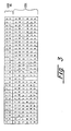
- TRIGMEM 92 of the present implementation is comprised of 8 8x1024 dual port Sub-Memories 102 through 116 and an 8 part AND Function 118 connected as shown in Fig. 4. As illustrated, the 80 address input lines from SYSBUS 18 are divided into 8 10-bit fields and the Trigger patterns are correspondingly divided into 8 8-bit sub-trigger fields wherein each sub-trigger field occupies one of Sub-Memories 102 through 116 and contains positions corresponding to each of Triggers A through H.
- TRIGMEM 92 detects the equivalence of a combination of bits on SYSBUS 18 with a trigger pattern stored in the 8 Sub-Memories 102-116 by associating each 10-bit address sub-field from SYSBUS 18 with a location in each of the 1024x8 submemories of TRIGMEM 92.
- the content of each such trigger sub-field location in Sub-Memories 102-116 will contain logic ones in the appropriate Trigger positions if the SYSBUS 18 address sub-field corresponds to a SYSBUS 18 condition to be detected, or if the particular trigger subfield is determined to be a "don't care" condition.
- TRIGMEM 92 is to provide Trigger A as an output when the condition (a)00010000 (b)00000000 (c)10000000 (d)00000000 (e)11000000 (f)00000000 (g)11111111 (h)00110000 (i)00000000 (j)11100011 occurs on SYSBUS 118 occurs. Ignoring the possibility of "don't care" states, the trigger pattern for this condition will then comprise:
- a trigger pattern for one or more of Triggers A through H is generated and loaded into TRIGMEM 92 is illustrated in Fig. 5. As indicated, this process is comprised of two stages.
- the first stage is the generation of a User Map 120 in which the conditions, or signals, present on each of SYSBUS 118's 80 lines are specified for each of Triggers A through H which are to be generated.
- This portion of the process is illustrated by the upper portion of Fig. 4, which represents a User Map 120.
- a User Map 120 contains 8 rows, one for each of Triggers A through H, and 80 columns, one for each of the lines of SYSBUS 18.
- Triggers A through H For each of Triggers A through H which are to be generated, the user first selects which trigger of Triggers A through H is being specified and then specifies the trigger condition for that trigger by defining a Boolean product function (an AND function) containing 1 to 80 terms wherein each term represents one of the 80 SYSBUS 18 signals that is to actively participate in generating the trigger. The user then assigns a state, logic 1 or logic 0, to each of the SYSBUS 18 signals, or lines, that is to define the trigger condition, depending upon whether the monitored condition requires that the signal on the corresponding line is to be a logic 1 or a logic 0. Signals not used in defining the trigger are assigned a "don't care" status. The addition of a "don't care" state to the trigger condition definitions, as well as logic 1 and logic 0 states, requires that the condition of each line, or signal, taking part in the definition of the trigger be defined by at least two bits.
- a Boolean product function an AND function
- Hardware Map 122 represents the actual trigger patterns to be stored in TRIGMEM 92.
- Hardware Map 122 is structured into 8 blocks, corresponding respectively to the 8 Sub-Memories 102-116 comprising TRIGMEM 92 and the corresponding 8 groups of ten SYSBUS 18 lines, each of which are connected to the second port address inputs of Sub-Memories 102-116, that is, to TA of TRIGMEM 92.
- Each block of Hardware Map 122 is comprised of 8 columns, each column corresponding, as indicated, to one of Triggers A through H, and into 1024 rows wherein each row corresponds to one of the Sub-Memory 102-116 address locations separately addressable by the 10 bit address inputs from the blocks of SYSBUS 18 lines.
- the trigger patterns stored in Sub-Memories 102-116 that is, in the blocks of Hardware Map 122, are then generated by dividing each row of User Map 120 into eight 10 bit "fields", wherein each such "field” represents, for a given trigger, the Boolean combination of signals on a 10 line block of SYSBUS 18 that defines a part of the trigger condition for that trigger.
- Each such 10 bit “field” may assume 1024 different values, defining a corresponding 1024 different binary numbers, and each of these values is assigned, on a 1-to-1 basis, to a corresponding single bit location in the column of Hardware Map 122, the address of the single bit location corresponding to the "value" of the field.
- the location of any given "bit” in a column of Hardware Map 122 is thereby set to "1” if the binary address of its location in the column corresponds to value of a "field” from User Map 120.
- This mapping of triggers and trigger conditions from User Map 120 to trigger patterns in Hardware Map 122 is illustrated in Fig. 4 for a single 10 bit "field” from the specification of a trigger in User Map 120, showing how that field maps into a single address location in a single column one sub-memory block of Hardware Map 122.
- the resultant trigger pattern may then be written directly into TRIGMEM 92 or, more likely, will be stored in Memory 16 or RAM 30 of CSS 14 and written into TRIGMEM 92 before the monitoring operation begins. Also, as as described elsewhere herein, certain preselected and often used trigger patterns may be "permanently" stored in EPROM 34 of CSS 14 for use when selected by a user of Bus Monitor 12.
- TRIGDET 96 is an AND/OR function which compares the triggers provided from EXTTRG 42, ILGL/ER 94 and TRIGMEM 92 with the trigger enable codes provided by TRIGENR 90 and provides a trigger output, TRIGS, whenever there is a concurrence of a SYSTEM 10 condition, as evidenced by a corresponding Trigger, and a trigger enable code.
- TRIGREG 98 is provided to latch and store the Triggers causing the TRIGS output so that, as previously described, the Trigger or Triggers causing TRIGS may be stored in Silo Bank 40, together with the sample data from the various sampling points in System 10.
- Triggers may result from the time sequential occurrence of others of Triggers A through H and XD through XH. For this reason, TRIGREG 98 stores not only the Trigger or Triggers directly causing TRIGS, but the sequential occurrence of Triggers and provides this information back to TRIGDET 96. TRIGDET 96 will, in turn, generate a TRIGS upon the occurrence of a specified sequence of Triggers when such has been specified and enabled by the trigger enable codes.
- TRIGDET 96 and TRIGREG 98 In as much as the detailed design of and implementations of the logic necessary to perform the functions of TRIGDET 96 and TRIGREG 98, and the necessary operations performed by TRIGDET 96 and TRIGREG 98 are fully described and defined by the other portions of this description of Bus Monitor 12, such as the descriptions of TRIGENR 90 and the enabling codes stored therein and TRIGMEM 92 and the trigger patterns stored therein, TRIGDET 96 and TRIGREG 98 will not be described further herein.
- Bus Monitor 12 includes a set of Interrupt/ Pattern Programmable Registers (IPPR) 48 connected from CPUBUS 22 and to SYSBUS 18.
- IPPR 48 may be used by CSS 14 in a first mode to test SYSBUS 18 and system elements connected from SYSBUS 18 by allowing CSS 14 to write test patterns onto SYSBUS 18 through IPPR 48 under the control of CSS 14.
- CSS 14 may write selected commands into IPPR 40, such as a system or CPU interrupt command. These commands will reside in IPPR 40 until the occurrence of a TRIGS output from TRIGDET 96 and TRIGREG 98 and will be transferred onto SYSBUS 18 at that time. In the present implementation of Bus Monitor 12, this command is most usually a CPU 28 interrupt command that will suspend the operation then being executed by CPU 28, so that Monitor 12 may interrupt the operation of System 10.
- This interrupt command appears on SYSBUS 18, and at the end of the SYSBUS 18 cycle, which is terminated by the command.
- the block of information stored in SSL 50 in association with the events related to the monitored condition causing the trigger will, in this case, begin with the trigger itself and the then present conditions on SYSBUS 18 that were sampled as a result of that trigger condition, such as the states present on the lines of SYSBUS 18 during that SYSBUS 18 cycle, and will conclude with the interrupt command as the final entry, the interrupt command having been the final set of conditions, or state, appearing on SYSBUS 18.
- the interrupt command is also copied into the time stamp silo of PSL 52 and XSL 54, that is, into PTSL 66 and XTSL 70, if these silos are recording the event in which the interrupt command occurs.
- Trigger Control 38 includes a Time Stamp Generator (TSG) 100 which is essentially a counter which is initiated upon and by the occurrence of a TRIGS from TRIGDET 96 and TRIGREG 98.
- TSG 100 The count output of TSG 100 is written into SSL 50 at the start of each sampling operation after the occurrence of a trigger, at the same address location as the data from SYSBUS 18 being recorded in SSL 50, and is provided so that a user of Bus Monitor 12 may determine the relative times of occurrence of each trigger condition.
- the count from TSG 100 is also written into PSL 52 and XSL 54, depending upon which of the portions of Silo Bank 40 are recording data in a given sampling operation of Bus Monitor 12, to aid in correlating the data stored in SSL 50, PSL 52 and XSL 54.
- the time stamp counts are again written into PSL 52 and XSL 54 at the same addresses as the data being concurrently recorded thereion.
- Time Stamp Generator is a 32 bit synchronous, wrap around counter clocked at 16 MHz and the low order 17 bits of Time Stamp Generator 100's count are written into STSL 62 while the low order 22 bits are written into PTSL 66 and XTSL 70.
- the recording of the time stamp count in SSL 50 and portions of the time stamp count in PSL 52 and XSL 54 is desirable because the writing of sampled data into the three subbanks of Silo Bank 40 are not correlated in themselves. That is, and for example, the various monitoring and sampling operations do not all result in data being written into all three portions of Silo Bank 40 in each operation, so that the blocks of information occupying similar address locations in the three subbanks of Silo Bank 40 are not necessarily from the same sampling operation. For example, if SYSBUS 18 is monitored for a condition which is of interest only with respect to SYSBUS 18, the occurrence of that condition would result in data being written only into SSL 50.
- a command for a data read from Memory 16 may occupy only a single SYSBUS 18 cycle, but the actual read of the data from Memory 16 through PBUS 20 will occupy 8 consecutive PBUS 20 cycles. Therefore, if that particular operation results in a trigger condition and the recording of data into Silo Bank 40, Silo Bank 40 must record the data from one SYSBUS 18 cycle in SSL 50 and the data from 8 consecutive PBUS 20 cycles in PSL 52 and CNTLTMG 88 must correspondingly generate 8 read cycles to PSL 52 for each single read cycle to SSL 50.
- the relationship between the data recorded in XSL 54 and that recorded in SSL 50 and PSL 52 will depend upon source of the data entered into XSL 54, but will be similar in nature to that between SSL 50 and PSL 52; accordingly, the following will describe the method for correlating the data stored in SSL 50, PSL 52 and XSL 54 using SSL 50 and PSL 52 as the example.
- the data recorded in SSL 50 or PSL 52 may assume either of the configurations illustrated in Fig. 6, which shows possible configurations of the data residing in the silo banks after two trigger events. It is assumed in Fig. 6 that the older data is toward the top of the Figure while newer data is entered at the bottom.
- System 10 that is, CSS 14 must locate and save two addresses for each of the silos, the first being the address of the silo entry containing the "final trigger', that is, the point of the interrupt command.
- the second address to locate in each silo is the address of the "final valid entry", that is, the values in the SYSBUS 18 and PBUS 20 silo address registers, that is, the ADRRC 80's of their respective SBMI 74 and PBMI 76, at the point recording stopped.
- Bus Monitor 12 is operating with the three silos independently capturing and recording data
- the data being recorded in the silos will be uncorrelated with respect to the respective silo addresses.
- a trigger will occur and will be recorded in the three silos, as described.
- the trigger will be recorded continuously in each successive address location of the silos until either the trigger is reset, to prepare the monitor for a next monitoring operation, or the silos are frozen for examination.
- the user will then search the silos, for example, SSL 50, to locate the recorded trigger of interest and will trace that trigger recording back through the silo to the first appearance of the trigger in the silo data, that is, the start of the recording due to that trigger.
- the silos for example, SSL 50
- the user may attempt to locate and trace the recorded trigger indication each of the other silos, or may trace back through the recorded time stamps in the other silos to a time stamp which is closest to that found with the start of the trigger as originally searched.
- the choice must be made as to which view of the recorded data is to be examined, the events preceding the triggers or the events following the triggers. If the pre-trigger events are to be examined, the recorded data is scanned in the direction of decreasing addresses and, if the post-trigger data is to be examined, in the direction of increasing addresses. The scanning and examination of recorded data continues until the "final entry" is found in each silo.
- the provision of time stamps with the recorded data allows the relative times of events to be determined from silo to silo, that is, allows the sequence of events are recorded in the silos to be placed in time relationship with one another so that, for example, the user may determine the relationship between an event recorded from PBUS 20 and the related events on SYSBUS 18.
Landscapes
- Engineering & Computer Science (AREA)
- General Engineering & Computer Science (AREA)
- Theoretical Computer Science (AREA)
- Computer Hardware Design (AREA)
- Quality & Reliability (AREA)
- Physics & Mathematics (AREA)
- General Physics & Mathematics (AREA)
- Debugging And Monitoring (AREA)
- Alarm Systems (AREA)
Applications Claiming Priority (8)
| Application Number | Priority Date | Filing Date | Title |
|---|---|---|---|
| US45566889A | 1989-12-22 | 1989-12-22 | |
| US455664 | 1989-12-22 | ||
| US455668 | 1989-12-22 | ||
| US07/455,664 US5142673A (en) | 1989-12-22 | 1989-12-22 | Bus monitor with dual port memory for storing selectable trigger patterns |
| US455666 | 1989-12-22 | ||
| US07/455,667 US5210862A (en) | 1989-12-22 | 1989-12-22 | Bus monitor with selective capture of independently occuring events from multiple sources |
| US455667 | 1989-12-22 | ||
| US07/455,666 US5206948A (en) | 1989-12-22 | 1989-12-22 | Bus monitor with means for selectively capturing trigger conditions |
Publications (3)
| Publication Number | Publication Date |
|---|---|
| EP0434081A2 true EP0434081A2 (de) | 1991-06-26 |
| EP0434081A3 EP0434081A3 (en) | 1992-04-15 |
| EP0434081B1 EP0434081B1 (de) | 1996-03-20 |
Family
ID=27504018
Family Applications (1)
| Application Number | Title | Priority Date | Filing Date |
|---|---|---|---|
| EP19900125077 Expired - Lifetime EP0434081B1 (de) | 1989-12-22 | 1990-12-21 | Überwachungsgerät zur selektiven Feststellung von einem Signalzustand in einem Betriebssystem |
Country Status (4)
| Country | Link |
|---|---|
| EP (1) | EP0434081B1 (de) |
| AU (1) | AU628244B2 (de) |
| DE (1) | DE69026048T2 (de) |
| ES (1) | ES2084644T3 (de) |
Cited By (2)
| Publication number | Priority date | Publication date | Assignee | Title |
|---|---|---|---|---|
| FR2721725A1 (fr) * | 1994-06-23 | 1995-12-29 | Matra Marconi Space France | Module de test pour analyser l'exécution d'un programme par une carte à microprocesseur. |
| GB2400469A (en) * | 2003-04-07 | 2004-10-13 | Sun Microsystems Inc | Generating and managing a knowledge base in a computer |
Family Cites Families (2)
| Publication number | Priority date | Publication date | Assignee | Title |
|---|---|---|---|---|
| US4731768A (en) * | 1986-09-15 | 1988-03-15 | Tektronix | Autoranging time stamp circuit |
| US4872121A (en) * | 1987-08-07 | 1989-10-03 | Harris Corporation | Method and apparatus for monitoring electronic apparatus activity |
-
1990
- 1990-12-11 AU AU67952/90A patent/AU628244B2/en not_active Ceased
- 1990-12-21 DE DE1990626048 patent/DE69026048T2/de not_active Expired - Fee Related
- 1990-12-21 ES ES90125077T patent/ES2084644T3/es not_active Expired - Lifetime
- 1990-12-21 EP EP19900125077 patent/EP0434081B1/de not_active Expired - Lifetime
Cited By (2)
| Publication number | Priority date | Publication date | Assignee | Title |
|---|---|---|---|---|
| FR2721725A1 (fr) * | 1994-06-23 | 1995-12-29 | Matra Marconi Space France | Module de test pour analyser l'exécution d'un programme par une carte à microprocesseur. |
| GB2400469A (en) * | 2003-04-07 | 2004-10-13 | Sun Microsystems Inc | Generating and managing a knowledge base in a computer |
Also Published As
| Publication number | Publication date |
|---|---|
| DE69026048T2 (de) | 1997-01-02 |
| EP0434081A3 (en) | 1992-04-15 |
| AU6795290A (en) | 1991-06-27 |
| EP0434081B1 (de) | 1996-03-20 |
| ES2084644T3 (es) | 1996-05-16 |
| DE69026048D1 (de) | 1996-04-25 |
| AU628244B2 (en) | 1992-09-10 |
Similar Documents
| Publication | Publication Date | Title |
|---|---|---|
| US5210862A (en) | Bus monitor with selective capture of independently occuring events from multiple sources | |
| US5226153A (en) | Bus monitor with time stamp means for independently capturing and correlating events | |
| US5206948A (en) | Bus monitor with means for selectively capturing trigger conditions | |
| US4327408A (en) | Controller device with diagnostic capability for use in interfacing a central processing unit with a peripheral storage device | |
| US4835675A (en) | Memory unit for data tracing | |
| US4654787A (en) | Apparatus for locating memory modules having different sizes within a memory space | |
| RU2137182C1 (ru) | Выполнение инструкции обработки данных | |
| EP0595036A1 (de) | DNA-Steuerung mit Speichertest-Möglichkeit | |
| KR100495755B1 (ko) | 미리 정의된 정지점 조건의 발생시에 신호를 감시하는메모리를 이용하는 디지털 회로 | |
| US5142673A (en) | Bus monitor with dual port memory for storing selectable trigger patterns | |
| EP0434081B1 (de) | Überwachungsgerät zur selektiven Feststellung von einem Signalzustand in einem Betriebssystem | |
| JPS5840772B2 (ja) | デ−タ比較一致表示方式 | |
| JPS5939783B2 (ja) | 論理状態追跡装置 | |
| SU1525678A1 (ru) | Микропроцессорна система дл программного управлени технологическим оборудованием | |
| JP2534314B2 (ja) | 半導体集積回路 | |
| JPS6153579A (ja) | 論理回路機能試験機 | |
| JPH04336630A (ja) | アドレストレース方法およびアドレストレース装置 | |
| JPH05324396A (ja) | プログラム走行履歴記録方式 | |
| JPS6237748A (ja) | フア−ムウエアによるトリガ信号発生方式 | |
| JPS61815A (ja) | シ−ケンス回路の異常個所発見装置 | |
| JPS6398751A (ja) | メモリ診断方式 | |
| JPH06119258A (ja) | 共通バスのトレースマーキング回路 | |
| JPH02500143A (ja) | コンピユータ・システム | |
| JPS63158637A (ja) | メモリトレ−ス方式 | |
| JPS61193190A (ja) | 表示制御装置 |
Legal Events
| Date | Code | Title | Description |
|---|---|---|---|
| PUAI | Public reference made under article 153(3) epc to a published international application that has entered the european phase |
Free format text: ORIGINAL CODE: 0009012 |
|
| AK | Designated contracting states |
Kind code of ref document: A2 Designated state(s): DE ES FR GB IT |
|
| PUAL | Search report despatched |
Free format text: ORIGINAL CODE: 0009013 |
|
| AK | Designated contracting states |
Kind code of ref document: A3 Designated state(s): DE ES FR GB IT |
|
| 17P | Request for examination filed |
Effective date: 19921013 |
|
| RAP1 | Party data changed (applicant data changed or rights of an application transferred) |
Owner name: BULL HN INFORMATION SYSTEMS INC. |
|
| 17Q | First examination report despatched |
Effective date: 19950424 |
|
| RAP1 | Party data changed (applicant data changed or rights of an application transferred) |
Owner name: BULL HN INFORMATION SYSTEMS INC. |
|
| GRAH | Despatch of communication of intention to grant a patent |
Free format text: ORIGINAL CODE: EPIDOS IGRA |
|
| GRAA | (expected) grant |
Free format text: ORIGINAL CODE: 0009210 |
|
| AK | Designated contracting states |
Kind code of ref document: B1 Designated state(s): DE ES FR GB IT |
|
| ITF | It: translation for a ep patent filed | ||
| REF | Corresponds to: |
Ref document number: 69026048 Country of ref document: DE Date of ref document: 19960425 |
|
| REG | Reference to a national code |
Ref country code: ES Ref legal event code: FG2A Ref document number: 2084644 Country of ref document: ES Kind code of ref document: T3 |
|
| ET | Fr: translation filed | ||
| PLBE | No opposition filed within time limit |
Free format text: ORIGINAL CODE: 0009261 |
|
| STAA | Information on the status of an ep patent application or granted ep patent |
Free format text: STATUS: NO OPPOSITION FILED WITHIN TIME LIMIT |
|
| 26N | No opposition filed | ||
| PGFP | Annual fee paid to national office [announced via postgrant information from national office to epo] |
Ref country code: ES Payment date: 19981223 Year of fee payment: 9 |
|
| PG25 | Lapsed in a contracting state [announced via postgrant information from national office to epo] |
Ref country code: ES Free format text: LAPSE BECAUSE OF NON-PAYMENT OF DUE FEES Effective date: 20001222 |
|
| REG | Reference to a national code |
Ref country code: GB Ref legal event code: IF02 |
|
| REG | Reference to a national code |
Ref country code: ES Ref legal event code: FD2A Effective date: 20010113 |
|
| PGFP | Annual fee paid to national office [announced via postgrant information from national office to epo] |
Ref country code: GB Payment date: 20051125 Year of fee payment: 16 |
|
| PGFP | Annual fee paid to national office [announced via postgrant information from national office to epo] |
Ref country code: DE Payment date: 20051130 Year of fee payment: 16 |
|
| PGFP | Annual fee paid to national office [announced via postgrant information from national office to epo] |
Ref country code: IT Payment date: 20061231 Year of fee payment: 17 |
|
| PG25 | Lapsed in a contracting state [announced via postgrant information from national office to epo] |
Ref country code: DE Free format text: LAPSE BECAUSE OF NON-PAYMENT OF DUE FEES Effective date: 20070703 |
|
| GBPC | Gb: european patent ceased through non-payment of renewal fee |
Effective date: 20061221 |
|
| PG25 | Lapsed in a contracting state [announced via postgrant information from national office to epo] |
Ref country code: GB Free format text: LAPSE BECAUSE OF NON-PAYMENT OF DUE FEES Effective date: 20061221 |
|
| PGFP | Annual fee paid to national office [announced via postgrant information from national office to epo] |
Ref country code: FR Payment date: 20061228 Year of fee payment: 17 |
|
| REG | Reference to a national code |
Ref country code: FR Ref legal event code: ST Effective date: 20081020 |
|
| PG25 | Lapsed in a contracting state [announced via postgrant information from national office to epo] |
Ref country code: FR Free format text: LAPSE BECAUSE OF NON-PAYMENT OF DUE FEES Effective date: 20071231 |
|
| PG25 | Lapsed in a contracting state [announced via postgrant information from national office to epo] |
Ref country code: IT Free format text: LAPSE BECAUSE OF NON-PAYMENT OF DUE FEES Effective date: 20071221 |