EP0436024B1 - Imprimante matricielle a diodes electroluminescentes - Google Patents
Imprimante matricielle a diodes electroluminescentes Download PDFInfo
- Publication number
- EP0436024B1 EP0436024B1 EP89910185A EP89910185A EP0436024B1 EP 0436024 B1 EP0436024 B1 EP 0436024B1 EP 89910185 A EP89910185 A EP 89910185A EP 89910185 A EP89910185 A EP 89910185A EP 0436024 B1 EP0436024 B1 EP 0436024B1
- Authority
- EP
- European Patent Office
- Prior art keywords
- data
- led
- print head
- led array
- serial
- Prior art date
- Legal status (The legal status is an assumption and is not a legal conclusion. Google has not performed a legal analysis and makes no representation as to the accuracy of the status listed.)
- Expired - Lifetime
Links
Images




Classifications
-
- B—PERFORMING OPERATIONS; TRANSPORTING
- B41—PRINTING; LINING MACHINES; TYPEWRITERS; STAMPS
- B41J—TYPEWRITERS; SELECTIVE PRINTING MECHANISMS, i.e. MECHANISMS PRINTING OTHERWISE THAN FROM A FORME; CORRECTION OF TYPOGRAPHICAL ERRORS
- B41J2/00—Typewriters or selective printing mechanisms characterised by the printing or marking process for which they are designed
- B41J2/435—Typewriters or selective printing mechanisms characterised by the printing or marking process for which they are designed characterised by selective application of radiation to a printing material or impression-transfer material
- B41J2/447—Typewriters or selective printing mechanisms characterised by the printing or marking process for which they are designed characterised by selective application of radiation to a printing material or impression-transfer material using arrays of radiation sources
- B41J2/45—Typewriters or selective printing mechanisms characterised by the printing or marking process for which they are designed characterised by selective application of radiation to a printing material or impression-transfer material using arrays of radiation sources using light-emitting diode [LED] or laser arrays
-
- G—PHYSICS
- G06—COMPUTING OR CALCULATING; COUNTING
- G06K—GRAPHICAL DATA READING; PRESENTATION OF DATA; RECORD CARRIERS; HANDLING RECORD CARRIERS
- G06K15/00—Arrangements for producing a permanent visual presentation of the output data, e.g. computer output printers
- G06K15/02—Arrangements for producing a permanent visual presentation of the output data, e.g. computer output printers using printers
- G06K15/12—Arrangements for producing a permanent visual presentation of the output data, e.g. computer output printers using printers by photographic printing, e.g. by laser printers
- G06K15/1238—Arrangements for producing a permanent visual presentation of the output data, e.g. computer output printers using printers by photographic printing, e.g. by laser printers simultaneously exposing more than one point
- G06K15/1242—Arrangements for producing a permanent visual presentation of the output data, e.g. computer output printers using printers by photographic printing, e.g. by laser printers simultaneously exposing more than one point on one main scanning line
- G06K15/1247—Arrangements for producing a permanent visual presentation of the output data, e.g. computer output printers using printers by photographic printing, e.g. by laser printers simultaneously exposing more than one point on one main scanning line using an array of light sources, e.g. a linear array
Definitions
- the present invention relates to an LED array printer which prints given characters and graphics on paper or the like with the use of, for example, electrophotographic technology.
- An LED array printer employs such an arrangement that light emitted from an LED array print head is transmitted through an rod lens array and irradiated onto a photosensitive drum so as to obtain an electrostatic latent image which is then developed into a toner image by a developing unit and is then transferred onto paper by a transfer unit.
- the photosensitive drum is charged to a predetermined potential by a charger, and is irradiated with light corresponding to predetermined data.
- An LED array print head includes a plurality of array chips and an LED driver for driving the array chips, mounted on a substrate, and is driven by signals transmitted between itself and a control circuit.
- the control circuit for controlling the LED array print head is connected to the LED array print head through connectors and a connecting cord, and includes a logic circuit for controlling the timing of data provided to the LED print head, a CPU, memory storing therein a control program for printing, data and the like, and a switch array for setting several kinds of modes.
- the switch array is used to set parameter information relating to the specification of the LED array print head, dispersion of characteristics and the like.
- the CPU detects the turn-on and -off of the switch array and produces the parameter information corresponding to the result of the turn-on and -off so as to control the logic circuit.
- the LED array chips having a large division number are used in order to increase the dot resolution so as to enhance the quality of printing, and further, the number of the array chips has to be increased in order to enable printing on a large size of paper.
- this causes higher cost, and further, the power consumption increases. Accordingly, such an LED printer is in general designed in order to have a specification which copes with specific needs or demands.
- Document EP-A-0 042 206 discloses an electronic printer having a print wheel which is replaceable. Since various types of print wheels can be used, each print wheel is provided with a memory unit where its print characteristics are stored. Thus, each print wheel carries information unique to that particular print wheel. A controller in the printer reads the contents of the memory unit and uses this information to generate print information during operation of the printer.
- the present invention provides an LED array printer comprising an LED array print head in which a plurality of LED array chips are arranged, and a control circuit for controlling the LED array print head, wherein a setting means for setting data in accordance with the type of the LED print head is provided in the LED array print head, and a data reading means for reading data from the setting means to control the LED array print head is provided in the control circuit.
- the above-mentioned setting means comprises a switch array, bonding wires, short wires and the like, and is disposed in the LED print head itself. Accordingly, it is possible to set printing control data corresponding to the characteristics and the specification of the LED array print head in the combination between the control circuit and the LED array print head without fail, thereby it is possible to eliminate inaccurate printing, inferior quality of printing, a failure of the print head and the like.
- Fig. 1 which is a block diagram showing an arrangement attaining a control principle of an LED array print head 1 according to the present invention
- a control circuit board 31 having a logic circuit 32 for controlling the timing of data fed to an LED array print head 1, a CPU 33 for controlling the transmission of data and commands between itself and a host printer controller 38 and the transmission of data and signals between itself and the LED array print head 1, and for controlling the operation of printing, and memory 34 used for storing therein a control program for the CPU 33, data and the like.
- Reference numeral 36 denotes a line through which signals are provided to the LED array print head, including signal lines SD, SCLK, LT, STB, a power line from a power source Vcc, a ground wire and the like.
- Reference numeral 37 is a video signal line for printing data, which feeds data that is processed and edited by the printer controller 38 to the logic circuit 32.
- a setting means 41 for setting the characteristics and the specification of the LED array print head 1 is disposed in the LED array print head 1. Further, the setting means 41 is connected to the CPU 33 through a line 42.
- the CPU 33 Upon energization of the power source, the CPU 33 at first reads the content of setting in the setting means 41 under a program which has been previously stored in the memory 34. Then, the CPU 33 reads corresponding parameters from the memory 34 in accordance with the read data or computes them, and sets them as print control information. Further, it drives and controls the LED array print head 1 through the intermediary of the logic circuit 32.
- the setting in the setting means 41 is made concerning characteristics, a specification and the like of an LED print head 1 to be mounted, at the time of manufacturing of the LED print head 1. Accordingly, there is no risk of erroneously setting the printing control information.
- Fig. 2 shows a first embodiment of the present invention.
- a switch array 51 having two switches 52, 53 is used as the setting means 41.
- One of the switches 52, 53 is grounded, and the other one of them is connected to the CPU 33 through the line 42 and is connected to the power source having a predetermined voltage Vcc through pull-up resistors 54, 55.
- the memory 34 on the control board 31 has been previously stored therein with a table such as, for example, Table 1. TABLE 1 SWITCH NO.
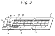
- Fig. 3 shows an arrangement of the above-mentioned LED array print head 1.
- Reference numeral 11 denotes a circuit board on which a plurality of LED array chips 12 are linearly arrayed. The above-mentioned chips 12 emit light in the direction of the arrow a in the figure.
- Reference numeral 13 denotes an LED driver 13 composed of a serial/parallel converting circuit for data, a register for holding data which has been subjected to parallel conversion, a print timing data circuit and a drive transistor which delivers a light emission drive current to the LED in accordance with an output of this gate circuit.
- the LED array chips 12 and the LED driver are connected together by bonding wires 14.
- Reference numeral 15 denotes a printed circuit pattern for feeding a power source and signals
- reference numeral 16 denotes a connector which is connected to the printer controller 38.
- a switch array 51 of the LED array print head 1 is disposed in the vicinity of the connector 16, and is set as to their turn-on and turn-off upon manufacture thereof. Accordingly, in the case of connecting this LED print head 1 to the control circuit board 31, data indicating the specification and the characteristics of this print head has been already set, and parameter information can be set by simply connecting the control circuit board 31 to the LED print head 1.
- Fig. 4 shows a second embodiment of the present invention.
- the setting means 41 is composed of short wires 61, 62. Since the setting in the setting means 41 is made for the LED array print head 1 on which the short wires are mounted, it is not always necessary to be variable. Accordingly, it is possible to fix the setting by means of the short wires 61, 62. Accordingly, upon manufacture of the LED array print head 1, the short wires 61, 62 can be soldered together with a connector 16 and the like as shown in Fig. 5. It is possible to use bonding wires, instead of the short wires.
- Fig. 6 shows a third embodiment of the present invention.
- the LED array print head 1 is mounted thereon with a parallel/serial converter IC 71 which incorporates a pull-up resistor 72 and the like, in addition to a switch array 73 used as the setting means 41.
- control board 31 is provided thereon with OR gates 75, 76 so that a serial clock signal and a latch signal can be delivered from not only the logic circuit 32 but also a microcontroller 74 corresponding to the CPU 33, Further, the wires SCLK, LT, GND are connected to the parallel/serial converting IC 71 by means of the LED driver 13, and an output from the parallel/serial converting IC 71 is delivered to the microcontroller 74 through the wire RD.
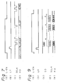
- the microcontroller 74 for controlling the logic circuit 32 sets a control (L-EN) signal (Fig. 7(a)) to a logic 1 so as to inhibit its operation, and thereafter, delivers a latch (LT) signal (Fig. 7(b)).
- This latch signal is delivered to the parallel/serial converting IC 71 through the OR gate 76, the wire LT and the LED driver 13.
- the parallel/serial converting IC 71 latches a parallel signal from the switch array 73 on its incorporated shift register when the latch signal is delivered.
- the microcontroller 74 delivers a certain number of serial clock (SCLK) signals (Fig.
- serial clock signals are delivered to the parallel/serial converting IC 71 through the OR gate 75, the wire SCLK, the LED driver 13.
- the parallel/serial converting IC 71 turns the set data from the switch array 73, which has been latched on its incorporated shift register, into a serial signal (Fig. 7(d)) when it receives the serial clock signal, and delivers the same to the microcontroller 74 through the wire RD.
- the microcontroller inverts the control (L-EN) signal into a logic 0.
- the logic circuit 32 falls in an operative condition, and accordingly, the serial data (SD) signal, the serial clock (SCLK) signal, the latch (LT) signal and the strobe (STB) signal are fed to the wires SD, SCLK, LT, STB, respectively, so as to carry out normal printing.
- the signal delivered to the microcontroller 74 through the wire RD is set as invalid data.
- the number of wires in the pattern on the board 11 of the LED array printer head 1 can be smaller than that in the first and second embodiment in which the data are red as parallel signals, and further, the number of pins for reading the set data, of the connector 16 which is connected to the control circuit board 31 can be decreased (to only one, that is, the wire RD alone). Accordingly, the package space can be reduced further, and the cost can be reduced.
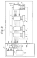
- Fig. 8 shows a fourth embodiment of the present invention.
- the wire SD is connected to the parallel/serial converting IC 71 by means of the LED driver 13, and simultaneously, an OR gate 81 is provided on the control board 31 so that the serial data (SD) signal is delivered from not only the logic signal 32 but also the microcontroller 74.
- the other arrangements are similar to those in the third embodiment.
- the microcontroller 74 sets at first a control (L-EN) signal (Fig. 9(a)) as a logic 1 so as to set the logic circuit 32 in a nonenergized condition, and thereafter, delivers a latch (LT) signal (Fig. 9(b)). At this time, the latching of the setting of the switch array on the shift register in the serial/parallel converting IC 71 is the same as that in the third embodiment.
- L-EN control
- LT latch
- the microcontroller 74 delivers a two bit checking serial data (SD) signal (Fig. 9 (c)), and simultaneously, delivers a number (m+n+2) of serial clock (SCLK) signals (Fig. 9 (d)).
- SD serial data
- SCLK serial clock
- the parallel/serial converting IC 71 delivers a predetermined data (RD) signal (Fig. 9 (e) to the microcontroller 74 through the wire RD in synchronisation with the delivered serial clock signal, Since the number of the serial clocks are regulated as mentioned above, the set data on the switch array 73 is read in synchronization with the number n of the serial clocks next to the number m if the LED driver is properly connected, and further, data which is read in synchronization with the last two serial clocks becomes the checking data. If the checking data is not read in synchronization with the last two serial clocks, it can be said that the LED driver is not properly connected.
- RD predetermined data
- the set data can be read by way of a less number of the wires, and simultaneously, the connecting condition of the LED driver 13 can be tested.
- Fig. 10 shows a fifth embodiment of the present invention.
- the microcontroller 74 delivers a latch (LT) signal and a serial clock (SCLK) signal to the LED array print head 1 so as to read the setting by the switch array 73.
- the thus read data concerning resolution, a dot number, a data wire number and the like are also delivered to the printer controller 38 through a bidirectional command interface 91.
- the printer controller 38 processes printing data corresponding to these data.
- a frequency (rate) of a serial clock (SCLK) signal, time intervals per wire (line cycle period) and the like corresponding to the read resolution, dot number, data line numbers and the like have been previously stored.
- the microcontroller 74 sets the frequency of the serial clock (SCLK) signal and the number thereof per wire as those read from the table of the switch array 73.
- This serial clock (SCLK) signal is fed to the printer controller 38 and the LED array print head 1.
- the printer controller 38 feeds printing data to the logic circuit 32 on the control circuit board 31 by way of a data line 92 in synchronization with the serial clock (SCLK) signal delivered to the printer controller 38.
- the logic circuit 32 further delivers the thus received signal to the LED array print head 1 by way of a data line 93.
- the wire number of the data lines 92, 93 is set to one or two corresponding to data on the switch array 73. If erroneous operation is likely to occur since the frequency of the serial clock signal is high, data is fed alternately to these lines so that the apparent clock frequency can be lowered. If the frequency is low, only one of the data lines is used.
- the microcontroller 74 produces a pulse for every line cycle period, and delivers the same to the printer controller 38 by way of a line 94,
- the printer controller 38 delivers data per line to the logic circuit 32 in synchronization with the received pulse.
- the logic circuit 32 delivers the data to the LED array print head 1 in synchronization with the line cycle period.
- the microcontroller 74 controls a sheet feed system (which is not shown) in synchronization with this line cycle period.
- Table 2 exhibits examples of the specification of the LED array print head 1.
- heads are roughly classified into A4 (letter) size heads and B4 size heads in view of the sizes of sheets to be printed.
- A4 size heads There are shown five kinds of A4 size heads, and three kinds of B4 size heads. Since the size is determined directly from the combination between the resolution and the number of dots per line, it is not necessary to particularly provide set data indicating sizes. Since there are four kinds of resolution, such as 240, 300, 400 and 600 (dot/inch), the resolution is indicated by two bits.
- the numbers of dots which is obtained by multiplying a minimum unit of the LED array with an integer number, there are four kinds in the case of the A4 size, and three kinds in the case of the B5 size.
- the number of dots is indicated by six bits. Since the number of the data lines is one (row) or two (row), it is indicated by one bit. Accordingly, in this embodiment, nine switches are required in the switch array 73 in order to set these data.
- data concerning, for example, wavelengths of light emitted from the LEDs 21 and light emission efficiencies of the LEDs 212 may be set on the switch array 73.
- LED printers having different specifications can be readily arranged only by replacing LED print heads in accordance with the different specifications, it is possible to reduce the cost. Further, since, for the user, the several kinds of the printers can be used only by replacing the heads from one to another, it is possible to reduce the expense in comparison with such a case that several kinds of printers are purchased. Further, in the case of constituting a print head having a new specification, it can be attained only by changing software (firmware) on the memory 34, and accordingly, it is possible to shorten the time of research and development.
- switch array 73 in the third, fourth and fifth embodiments can be replaced with short wires, bonding wires or the like.
- SHEET SIZE RESOLUTION (dpi) DOT NUMBER/LINE WAY OF ARRANGEMENT 1 LETTER (A4) 240 2,048 ONE ROW 2 300 2,560 ONE ROW 3 400 3,450 ONE ROW 4 400 3,456 TWO ROWS 5 600 5,240 TWO ROWS 6 B4 240 2,432 ONE ROW 7 300 3,072 ONE ROW 8 400 4,096 TWO ROWS TABLE 3 NO.
- the LED array printer according to the present invention has, in its LED array print head, a means for setting data indicating a specification and characteristics of the head. Accordingly, it is possible to surely set parameter information for print control, corresponding to the specification and characteristics of the head, and therefore, it is useful for the guarantee of operation and the guarantee of printing quality for LED array printers in which several kinds of LED array print heads are combined with a common printer control circuit.
- printers having different specifications can be readily obtained by only replacement of print heads, it is useful for the provision of printers having various different specifications and for change in the specification of the printer.
Landscapes
- Physics & Mathematics (AREA)
- Optics & Photonics (AREA)
- Engineering & Computer Science (AREA)
- Health & Medical Sciences (AREA)
- General Health & Medical Sciences (AREA)
- Toxicology (AREA)
- General Engineering & Computer Science (AREA)
- General Physics & Mathematics (AREA)
- Theoretical Computer Science (AREA)
- Printers Or Recording Devices Using Electromagnetic And Radiation Means (AREA)
Abstract
Claims (5)
- Imprimante à diodes électroluminescentes comprenant
une tête d'impression (1) à diodes électroluminescentes comportant une pluralité de puces (12) à réseau de diodes électroluminescentes, cette tête d'impression à diodes électroluminescentes étant connectée à un panneau de commande (31) comportant un circuit de commande (32, 33), au moyen de lignes de signaux (36, 42) et d'une ligne de source d'alimentation,
caractérisée en ce que
ladite tête d'impression à diodes électroluminescentes comporte en outre un moyen (41) d'établissement de données pour établir des données en fonction du type de ladite tête d'impression à diodes électroluminescentes, dans laquelle un moyen de lecture utilisé dans ledit circuit de commande lit tout d'abord lesdites données établies en utilisant un programme de commande stocké dans une mémoire (34) disposée sur ledit panneau de commande, puis lit des paramètres en fonction desdites données établies à partir de ladite mémoire, ces paramètres étant associés aux spécifications et caractéristiques de ladite tête d'impression à diodes électroluminescentes et sont établis sous la forme d'information de commande d'impression dans ledit circuit de commande. - Imprimante à diodes électroluminescentes selon la revendication 1, dans laquelle ledit moyen (41) d'établissement de données comprend un réseau de commutateurs (51).
- Imprimante à diodes électroluminescentes selon la revendication 1 ou 2, dans laquelle ledit moyen (41) d'établissement de données comprend des fils courts ou des fils de liaison (61, 62).
- Imprimante à diodes électroluminescentes selon l'une quelconque des revendications précédentes, dans laquelle ledit moyen (41) d'établissement de données est réglé au cours de la fabrication.
- Imprimante à diodes électroluminescentes selon l'une quelconque des revendications précédentes, dans laquelle ladite tête d'impression (1) à diodes électroluminescentes comprend en outre un moyen de conversion (71) parallèle/série pour convertir des données en parallèle établies dans ledit moyen d'établissement (73) en données en série et pour délivrer lesdites données en série audit moyen de lecture de données.
Applications Claiming Priority (3)
| Application Number | Priority Date | Filing Date | Title |
|---|---|---|---|
| JP23679988 | 1988-09-21 | ||
| JP236799/88 | 1988-09-21 | ||
| PCT/JP1989/000940 WO1990003273A1 (fr) | 1988-09-21 | 1989-09-14 | Imprimante matricielle a diodes electroluminescentes |
Publications (3)
| Publication Number | Publication Date |
|---|---|
| EP0436024A1 EP0436024A1 (fr) | 1991-07-10 |
| EP0436024A4 EP0436024A4 (en) | 1992-04-08 |
| EP0436024B1 true EP0436024B1 (fr) | 1995-07-19 |
Family
ID=17005963
Family Applications (1)
| Application Number | Title | Priority Date | Filing Date |
|---|---|---|---|
| EP89910185A Expired - Lifetime EP0436024B1 (fr) | 1988-09-21 | 1989-09-14 | Imprimante matricielle a diodes electroluminescentes |
Country Status (4)
| Country | Link |
|---|---|
| US (1) | US5200763A (fr) |
| EP (1) | EP0436024B1 (fr) |
| DE (1) | DE68923559T2 (fr) |
| WO (1) | WO1990003273A1 (fr) |
Cited By (1)
| Publication number | Priority date | Publication date | Assignee | Title |
|---|---|---|---|---|
| US11652196B2 (en) | 2019-10-15 | 2023-05-16 | Samsung Electronics Co., Ltd. | Display module and manufacturing method thereof |
Families Citing this family (11)
| Publication number | Priority date | Publication date | Assignee | Title |
|---|---|---|---|---|
| JPH0511578A (ja) * | 1991-07-03 | 1993-01-22 | Toshiba Corp | 記録装置 |
| US5691750A (en) * | 1992-11-24 | 1997-11-25 | Lexmark International, Inc. | Ink level sensing for disposable ink jet print head cartridges |
| JPH10235935A (ja) * | 1997-02-27 | 1998-09-08 | Oki Data:Kk | ドライバicとledプリントヘッド |
| JP2001343803A (ja) * | 2000-06-01 | 2001-12-14 | Canon Inc | 画像形成装置 |
| JP4536523B2 (ja) * | 2005-01-11 | 2010-09-01 | 株式会社沖データ | 画像形成装置 |
| KR100782819B1 (ko) * | 2005-09-27 | 2007-12-06 | 삼성전자주식회사 | 어레이 헤드형 프린터 및 어레이 헤드형 프린터에 의한인쇄방법 |
| JP5200360B2 (ja) * | 2006-09-29 | 2013-06-05 | 富士ゼロックス株式会社 | 露光装置および画像形成装置 |
| US7737926B2 (en) * | 2006-11-24 | 2010-06-15 | Ascend Visual System, Inc. | Dynamic LED matrix lighting control using scanning architecture |
| TWI642979B (zh) | 2018-05-03 | 2018-12-01 | 達方電子股份有限公司 | 背光裝置 |
| US11710464B2 (en) | 2018-05-03 | 2023-07-25 | Darfon Electronics Corp. | Display device and backlight apparatus thereof |
| JP7589074B2 (ja) | 2021-03-12 | 2024-11-25 | キヤノン株式会社 | 素子基板、記録ヘッド、記録装置及びその制御方法 |
Family Cites Families (10)
| Publication number | Priority date | Publication date | Assignee | Title |
|---|---|---|---|---|
| JPS6310293Y2 (fr) * | 1979-08-21 | 1988-03-28 | ||
| CA1162317A (fr) * | 1980-04-28 | 1984-02-14 | Gordon Sohl | Cartouche a roue d'impression codee dotee d'une memoire morte |
| JPS58209578A (ja) * | 1982-05-31 | 1983-12-06 | Nec Corp | 感熱記録装置 |
| US4588883A (en) * | 1983-11-18 | 1986-05-13 | Eastman Kodak Company | Monolithic devices formed with an array of light emitting diodes and a detector |
| JPH07108573B2 (ja) * | 1986-05-21 | 1995-11-22 | 沖電気工業株式会社 | Ledアレイ駆動回路 |
| JPS6337970A (ja) * | 1986-08-01 | 1988-02-18 | Alps Electric Co Ltd | ドツトプリンタ |
| JPH0785937B2 (ja) * | 1986-09-12 | 1995-09-20 | 三菱電機株式会社 | ドライバic及び記録ヘッド |
| JP2832710B2 (ja) * | 1987-01-07 | 1998-12-09 | 沖電気工業 株式会社 | プリンタ |
| US4831395A (en) * | 1987-04-01 | 1989-05-16 | Eastman Kodak Company | Printer apparatus |
| US4746941A (en) * | 1987-10-13 | 1988-05-24 | Eastman Kodak Company | Dot printer with token bit selection of data latching |
-
1989
- 1989-09-14 US US07/668,492 patent/US5200763A/en not_active Expired - Lifetime
- 1989-09-14 EP EP89910185A patent/EP0436024B1/fr not_active Expired - Lifetime
- 1989-09-14 WO PCT/JP1989/000940 patent/WO1990003273A1/fr not_active Ceased
- 1989-09-14 DE DE68923559T patent/DE68923559T2/de not_active Expired - Lifetime
Cited By (1)
| Publication number | Priority date | Publication date | Assignee | Title |
|---|---|---|---|---|
| US11652196B2 (en) | 2019-10-15 | 2023-05-16 | Samsung Electronics Co., Ltd. | Display module and manufacturing method thereof |
Also Published As
| Publication number | Publication date |
|---|---|
| DE68923559T2 (de) | 1996-05-02 |
| EP0436024A1 (fr) | 1991-07-10 |
| DE68923559D1 (de) | 1995-08-24 |
| WO1990003273A1 (fr) | 1990-04-05 |
| EP0436024A4 (en) | 1992-04-08 |
| US5200763A (en) | 1993-04-06 |
Similar Documents
| Publication | Publication Date | Title |
|---|---|---|
| JP2755406B2 (ja) | データ・ラッチの選択用トークン・ビットを有するドットプリンタおよびそのプリンタに使用するドライバ回路 | |
| US7901022B2 (en) | Printing apparatus, printing method and data processing method for compensating for abnormal nozzles in accordance with priorities | |
| EP0436024A1 (fr) | Imprimante matricielle a diodes electroluminescentes | |
| US7075674B2 (en) | Image recording apparatus | |
| US7084996B2 (en) | Recording device | |
| EP1195256B1 (fr) | Tete d'impression thermique | |
| JP2023174522A (ja) | 光プリントヘッド及び光プリントヘッドを備える画像形成装置 | |
| US20240393712A1 (en) | Light-emitting device and image forming apparatus | |
| JP2024030133A (ja) | 露光装置及び画像形成装置 | |
| CN117434806A (zh) | 包括多个发光部分的发光芯片和图像形成装置 | |
| US7990409B2 (en) | Image forming apparatus | |
| EP0751003B1 (fr) | Imprimante avec tête d'impression amovible | |
| JP2710432B2 (ja) | プリンタ及びプリントヘッド | |
| US6022155A (en) | Driver IC and print head | |
| EP0537680B1 (fr) | Circuit de commande d'une tête d'impression thermique | |
| JP2634821B2 (ja) | 印字ヘッド | |
| JPS61234163A (ja) | Ledプリンタの印字制御方式 | |
| EP0185910A1 (fr) | Dispositif de commande pour imprimante thermique | |
| JPWO1990003273A1 (ja) | プリンタ及びプリントヘッド | |
| JP2911727B2 (ja) | プリンタの書込駆動回路 | |
| JP2783949B2 (ja) | Ledプリンタ | |
| JP2907143B2 (ja) | Ledプリンタ装置 | |
| JP2849244B2 (ja) | Ledヘッド及びledヘッド光量パラメータ読出し装置 | |
| JP2008209776A (ja) | 画像形成装置および画像形成方法 | |
| JPS62216748A (ja) | 記録装置 |
Legal Events
| Date | Code | Title | Description |
|---|---|---|---|
| PUAI | Public reference made under article 153(3) epc to a published international application that has entered the european phase |
Free format text: ORIGINAL CODE: 0009012 |
|
| 17P | Request for examination filed |
Effective date: 19910320 |
|
| AK | Designated contracting states |
Kind code of ref document: A1 Designated state(s): DE FR GB |
|
| A4 | Supplementary search report drawn up and despatched |
Effective date: 19920218 |
|
| AK | Designated contracting states |
Kind code of ref document: A4 Designated state(s): DE FR GB |
|
| 17Q | First examination report despatched |
Effective date: 19931116 |
|
| GRAA | (expected) grant |
Free format text: ORIGINAL CODE: 0009210 |
|
| AK | Designated contracting states |
Kind code of ref document: B1 Designated state(s): DE FR GB |
|
| REF | Corresponds to: |
Ref document number: 68923559 Country of ref document: DE Date of ref document: 19950824 |
|
| ET | Fr: translation filed | ||
| PLBE | No opposition filed within time limit |
Free format text: ORIGINAL CODE: 0009261 |
|
| STAA | Information on the status of an ep patent application or granted ep patent |
Free format text: STATUS: NO OPPOSITION FILED WITHIN TIME LIMIT |
|
| 26N | No opposition filed | ||
| REG | Reference to a national code |
Ref country code: GB Ref legal event code: IF02 |
|
| PGFP | Annual fee paid to national office [announced via postgrant information from national office to epo] |
Ref country code: FR Payment date: 20080915 Year of fee payment: 20 |
|
| PGFP | Annual fee paid to national office [announced via postgrant information from national office to epo] |
Ref country code: GB Payment date: 20080917 Year of fee payment: 20 |
|
| PGFP | Annual fee paid to national office [announced via postgrant information from national office to epo] |
Ref country code: DE Payment date: 20080926 Year of fee payment: 20 |
|
| REG | Reference to a national code |
Ref country code: GB Ref legal event code: PE20 Expiry date: 20090913 |
|
| PG25 | Lapsed in a contracting state [announced via postgrant information from national office to epo] |
Ref country code: GB Free format text: LAPSE BECAUSE OF EXPIRATION OF PROTECTION Effective date: 20090913 |