EP0437939A1 - Integrierbarer DMOS-Transistor und Verfahren zu dessen Herstellung - Google Patents
Integrierbarer DMOS-Transistor und Verfahren zu dessen Herstellung Download PDFInfo
- Publication number
- EP0437939A1 EP0437939A1 EP90313365A EP90313365A EP0437939A1 EP 0437939 A1 EP0437939 A1 EP 0437939A1 EP 90313365 A EP90313365 A EP 90313365A EP 90313365 A EP90313365 A EP 90313365A EP 0437939 A1 EP0437939 A1 EP 0437939A1
- Authority
- EP
- European Patent Office
- Prior art keywords
- region
- layer
- type
- well
- doped
- Prior art date
- Legal status (The legal status is an assumption and is not a legal conclusion. Google has not performed a legal analysis and makes no representation as to the accuracy of the status listed.)
- Withdrawn
Links
Images






Classifications
-
- H—ELECTRICITY
- H10—SEMICONDUCTOR DEVICES; ELECTRIC SOLID-STATE DEVICES NOT OTHERWISE PROVIDED FOR
- H10D—INORGANIC ELECTRIC SEMICONDUCTOR DEVICES
- H10D30/00—Field-effect transistors [FET]
- H10D30/60—Insulated-gate field-effect transistors [IGFET]
- H10D30/64—Double-diffused metal-oxide semiconductor [DMOS] FETs
- H10D30/66—Vertical DMOS [VDMOS] FETs
-
- H—ELECTRICITY
- H10—SEMICONDUCTOR DEVICES; ELECTRIC SOLID-STATE DEVICES NOT OTHERWISE PROVIDED FOR
- H10D—INORGANIC ELECTRIC SEMICONDUCTOR DEVICES
- H10D30/00—Field-effect transistors [FET]
- H10D30/01—Manufacture or treatment
- H10D30/021—Manufacture or treatment of FETs having insulated gates [IGFET]
- H10D30/028—Manufacture or treatment of FETs having insulated gates [IGFET] of double-diffused metal oxide semiconductor [DMOS] FETs
- H10D30/0291—Manufacture or treatment of FETs having insulated gates [IGFET] of double-diffused metal oxide semiconductor [DMOS] FETs of vertical DMOS [VDMOS] FETs
-
- H—ELECTRICITY
- H10—SEMICONDUCTOR DEVICES; ELECTRIC SOLID-STATE DEVICES NOT OTHERWISE PROVIDED FOR
- H10D—INORGANIC ELECTRIC SEMICONDUCTOR DEVICES
- H10D30/00—Field-effect transistors [FET]
- H10D30/60—Insulated-gate field-effect transistors [IGFET]
- H10D30/64—Double-diffused metal-oxide semiconductor [DMOS] FETs
- H10D30/66—Vertical DMOS [VDMOS] FETs
- H10D30/663—Vertical DMOS [VDMOS] FETs having both source contacts and drain contacts on the same surface, i.e. up-drain VDMOS
-
- H—ELECTRICITY
- H10—SEMICONDUCTOR DEVICES; ELECTRIC SOLID-STATE DEVICES NOT OTHERWISE PROVIDED FOR
- H10D—INORGANIC ELECTRIC SEMICONDUCTOR DEVICES
- H10D84/00—Integrated devices formed in or on semiconductor substrates that comprise only semiconducting layers, e.g. on Si wafers or on GaAs-on-Si wafers
- H10D84/01—Manufacture or treatment
- H10D84/0107—Integrating at least one component covered by H10D12/00 or H10D30/00 with at least one component covered by H10D8/00, H10D10/00 or H10D18/00, e.g. integrating IGFETs with BJTs
- H10D84/0109—Integrating at least one component covered by H10D12/00 or H10D30/00 with at least one component covered by H10D8/00, H10D10/00 or H10D18/00, e.g. integrating IGFETs with BJTs the at least one component covered by H10D12/00 or H10D30/00 being a MOS device
-
- H—ELECTRICITY
- H10—SEMICONDUCTOR DEVICES; ELECTRIC SOLID-STATE DEVICES NOT OTHERWISE PROVIDED FOR
- H10D—INORGANIC ELECTRIC SEMICONDUCTOR DEVICES
- H10D84/00—Integrated devices formed in or on semiconductor substrates that comprise only semiconducting layers, e.g. on Si wafers or on GaAs-on-Si wafers
- H10D84/01—Manufacture or treatment
- H10D84/0123—Integrating together multiple components covered by H10D12/00 or H10D30/00, e.g. integrating multiple IGBTs
- H10D84/0126—Integrating together multiple components covered by H10D12/00 or H10D30/00, e.g. integrating multiple IGBTs the components including insulated gates, e.g. IGFETs
- H10D84/0135—Manufacturing their gate conductors
- H10D84/0142—Manufacturing their gate conductors the gate conductors having different shapes or dimensions
-
- H—ELECTRICITY
- H10—SEMICONDUCTOR DEVICES; ELECTRIC SOLID-STATE DEVICES NOT OTHERWISE PROVIDED FOR
- H10D—INORGANIC ELECTRIC SEMICONDUCTOR DEVICES
- H10D84/00—Integrated devices formed in or on semiconductor substrates that comprise only semiconducting layers, e.g. on Si wafers or on GaAs-on-Si wafers
- H10D84/01—Manufacture or treatment
- H10D84/02—Manufacture or treatment characterised by using material-based technologies
- H10D84/03—Manufacture or treatment characterised by using material-based technologies using Group IV technology, e.g. silicon technology or silicon-carbide [SiC] technology
- H10D84/038—Manufacture or treatment characterised by using material-based technologies using Group IV technology, e.g. silicon technology or silicon-carbide [SiC] technology using silicon technology, e.g. SiGe
-
- H—ELECTRICITY
- H10—SEMICONDUCTOR DEVICES; ELECTRIC SOLID-STATE DEVICES NOT OTHERWISE PROVIDED FOR
- H10D—INORGANIC ELECTRIC SEMICONDUCTOR DEVICES
- H10D84/00—Integrated devices formed in or on semiconductor substrates that comprise only semiconducting layers, e.g. on Si wafers or on GaAs-on-Si wafers
- H10D84/101—Integrated devices comprising main components and built-in components, e.g. IGBT having built-in freewheel diode
- H10D84/141—VDMOS having built-in components
- H10D84/148—VDMOS having built-in components the built-in components being breakdown diodes, e.g. Zener diodes
-
- H—ELECTRICITY
- H10—SEMICONDUCTOR DEVICES; ELECTRIC SOLID-STATE DEVICES NOT OTHERWISE PROVIDED FOR
- H10D—INORGANIC ELECTRIC SEMICONDUCTOR DEVICES
- H10D84/00—Integrated devices formed in or on semiconductor substrates that comprise only semiconducting layers, e.g. on Si wafers or on GaAs-on-Si wafers
- H10D84/40—Integrated devices formed in or on semiconductor substrates that comprise only semiconducting layers, e.g. on Si wafers or on GaAs-on-Si wafers characterised by the integration of at least one component covered by groups H10D12/00 or H10D30/00 with at least one component covered by groups H10D10/00 or H10D18/00, e.g. integration of IGFETs with BJTs
- H10D84/401—Combinations of FETs or IGBTs with BJTs
-
- H—ELECTRICITY
- H10—SEMICONDUCTOR DEVICES; ELECTRIC SOLID-STATE DEVICES NOT OTHERWISE PROVIDED FOR
- H10D—INORGANIC ELECTRIC SEMICONDUCTOR DEVICES
- H10D89/00—Aspects of integrated devices not covered by groups H10D84/00 - H10D88/00
- H10D89/60—Integrated devices comprising arrangements for electrical or thermal protection, e.g. protection circuits against electrostatic discharge [ESD]
- H10D89/601—Integrated devices comprising arrangements for electrical or thermal protection, e.g. protection circuits against electrostatic discharge [ESD] for devices having insulated gate electrodes, e.g. for IGFETs or IGBTs
- H10D89/611—Integrated devices comprising arrangements for electrical or thermal protection, e.g. protection circuits against electrostatic discharge [ESD] for devices having insulated gate electrodes, e.g. for IGFETs or IGBTs using diodes as protective elements
Definitions
- the present invention relates generally to the integration of semiconductor control and power devices, and methods of manufacturing same.
- bipolar power transistors were fabricated in bipolar form. This was largely due to the fact that bipolar power transistors emerged as a mature technology before the development of MOS Power devices. Power Bipolar devices have proved to be extremely rugged and have large power handling capabilities. The draw-back of bipolar power transistors is that they consume large amounts of power to turn the device on and off and are limited to switching speeds of the order of 50 KHz.
- the Power DMOS device has several advantages over its Bipolar counterpart.
- the Power DMOS device requires a lower power to switch the device on and off and contrary to the Bipolar device it does not require a steady state current to keep it switched on.
- the Power DMOS device is also capable of a lower series resistance than the Bipolar device which is limited in some circuits or modes to an inherent voltage drop of approximately 0.6 volt. The combination of the power drop across the device and the power required to drive the device allows the Powers DMOS device to dissipate much less heat than its Bipolar counterpart.
- the Power DMOS device being a majority carrier device, switches faster than its Bipolar counterpart and further the switching of its gate is compatible with the voltage available from MOS logic drive.
- the Power DMOS device also has advantages from a ruggedness point of view. Due to the Power DMOS positive temperature coefficient of on-state resistance in the linear region, lateral thermal instabilities do not occur in contrast to Bipolar devices where localised hot spots can cause current hogging and eventual device thermal runaway and breakdown. See for example, Fong et al, Power DMOS for High-Frequency and Switching Applications, 27 IEEE Tr.Elec.Dev. 322 (1980); Coen et al, A High-Performance Planar Power MOSFET, 27 IEEE Tr.Elec.Dev. 340 (1980); and Sun et al, Modeling of the On-Resistance of LDMOS, VDMOS, and VMOS Power Transistors, 27 IEEE Tr.Elec.Dev. 356 (1980).
- DMOS power structures with either or both bipolar or MOS control circuitry are commonly referred to as smart power or integrated power devices. These devices try to achieve the integration of bipolar and MOS technology, commonly referred to as BiCMOS technology, to form integrated circuit chips having power handling devices combined with logic and analog circuit functions. Multi-output power devices can be manufactured on the same silicon die with each power DMOS device totally insulated. Both the drain and the source of the DMOS devices are located on the top side of the silicon die.
- a smart power circuit which combines the use of DMOS devices with high voltage NPN and CMOS control logic circuitry is beneficial to the integrated circuit art. Furthermore, such a smart power circuit which could provide a DMOS power transistor which is as rugged if not more rugged than existing DMOS power structures would make such integrated circuit further beneficial.
- the present process employs a self-aligned Power DMOS cell which improves the ruggedness of the device making it less susceptible to secondary breakdown and improves the Safe Operating Area (SOA) of the device under both Reverse Bias and Forward Bias Safe Operating (RB-SOA and FBSOA) conditions experienced when driving inductive or commutating loads. Additionally, such a structure is fabricated by a process which if combined with the fabrication of bipolar logic circuitry would not degrade the operating characteristics of either the DMOS, PMOS or NMOS (CMOS) or the bipolar devices.
- SOA Safe Operating Area
- RB-SOA and FBSOA Forward Bias Safe Operating
- the process may employ a multi-epilayer structure to provide a single output device with the source and drain on opposite sides of the die and which is isolated from the control logic. Unidirectional current flow is achieved straight through the die resulting in a lower R DSon for a given device size.
- the present multiepitaxial process for fabricating a high power handling DMOS transistor concurrently with CMOS, PMOS and NMOS, control circuitry which is also compatible with the integration of bipolar devices, eliminates or reduces the disadvantages and shortcomings associated with known methods and structures.
- CMOS devices complementary metal-oxide-semiconductor
- bipolar devices NPN and PNP
- DMOS devices preserving good performance characteristics for the CMOS and bipolar devices plus ruggedness for the DMOS devices.
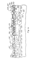
- Figures 1a-o illustrate in cross sectional elevation view steps of the first preferred embodiment method which integrates CMOS, NPN, PNP, and DMOS devices all with top side contacts. Simplified devices (i.e., single source and drain) are shown for clarity.
- the first preferred embodiment method includes the following steps:
- FIG 3 is a plan view that illustrates two adjacent DMOS cells 302 and 304 which have a common Poly 150 gate plus portions of two more DMOS cells 306 and 308 that are isolated by from cells 302 and 304 by field oxide 140 plus P+ isolation regions 130.
- the buried N+ layers 104 for cells 302 and 304 are contiguous but isolated from the buried N+ layers 104 for cells 306 and 308; this is analogous to the isolation of buried layer 108 from buried layers 106 and 110 shown in Figure 1o.
- Figure 4a depicts a schematic cross-section of a starting silicon substrate or wafer 12 which has a ⁇ 100 ⁇ crystal orientation, is highly impurity doped with N conductivity type donor atoms, and has a resistivity of less than 0.02 Ohm-cm.
- a first N-type epitaxial (epi) layer 14 is formed on wafer 12.
- Epitaxial layer 14 may be deposited or grown on wafer 12 by conventional and well known methods such as batch reactor or continuous chemical vapor deposition, metalorganic chemical vapor deposition (MOCVD), molecular beam epitaxy (MBE), etc. In a preferred embodiment a thickness of 20 ⁇ m and a resistivity of 2.5 ohm-cm is desired.
- MOCVD metalorganic chemical vapor deposition
- MBE molecular beam epitaxy
- the exposed surface of epi layer 14 is next thermally oxidized to form an oxide layer 16 with a thickness of approximately 6500 A.
- a layer of photoresist (not shown) is spun over oxide 16, and oxide 16 is then photolithographically patterned and exposed to open regions which are to contain the first buried region referred to herein as N Buried Layer (NBL) 24.
- NBL N Buried Layer
- an E-beam pattern can be used.
- the preference of photoresist or E-beam resist is immaterial to the present invention.
- the exposed portion of oxide 16 is removed by stripping in an HF bath or other well known method and subsequently the resist material is removed by stripping or other well known method.
- a pre-implant oxide is thermally grown in the exposed region to a thickness of approximately 500 A.
- the NBL region 24 is formed by a 60 KeV Phosphorus implant dose of approximately 1.0 ⁇ 1015 atoms/cm2 through the pre-implant oxide.
- the wafer is then subjected to a thermal diffusion for 800 minutes at 1200 C in an oxygen ambient. This forms a 9000 A oxide layer over NBL regions 24 and the diffusion has a sheet resistance of 35 ohms/square.
- the NBL layer is used under the Power DMOS device and is designed to minmize the series resistance to current flow between the subsequent DUF diffusion (explained infra ) and the N+ substrate 12.
- the oxide is then photolithographically patterned and etched to open regions for the second buried layer which is a P-type layer referred to as P-ground (PGND).
- a pre-implant oxide is thermally grown in the exposed region to a thickness of approximately 825 A. This region is then implanted with a Boron dose of 1 ⁇ 1014 atoms/cm2 at 60 KeV to form a layer 6 ⁇ m deep with a sheet resistance of 170 ohms/square. See Figure 4a.
- this second epitaxial layer 20 acts as the ground plane for the control circuitry and is analogous to the substrate 102 of the first preferred embodiment.
- the surface of the wafer is next oxidized to form a 6500 A oxide layer 22 over P-type epitaxial layer 20.
- Photoresist (not shown) is spun over the surface of the oxide and photolithographically patterned and exposed to form open regions 26 whereat buried N+ Diffusion Under Film (DUF) regions 48 are formed in the exposed region of the wafer.
- the DUF regions are fabricated using Antimony 27 implant dose of 2.1 ⁇ 1015 atoms/cm2 at 60 KeV energy followed by a 35 hours, 1250 C diffusion in a 10% oxygen atmosphere.
- the resultant DUF regions 48 have a sheet resistance of 25 ohms/square and oxide 34 thickness of 10,000 A. See Figure 4b. The sheet resistance is reduced during subsequent processing to 12 ohms/square.
- DUF regions examples are the DMOS vertical backside drain output which abuts NBL 24, NPN transistor collector contact, bipolar double diffused low voltage NPN transistor, bipolar high voltage lateral PNP transistor and PMOS transistors.
- a DUF may be used in a portion of the control circuitry to reduce lateral resistance within a surface tank or to inhibit the punchthrough of surface devices to the underlying P-epi layer.
- PBLs P-type buried layers 42, referred to herein as PBLs, will be formed in P-epi layer 20.
- the PBLs are formed by a Boronw implant dose of 5.0 ⁇ 1014 atoms/cm2 at 50 KeV through a 825 A preimplant oxide formed on the surface of the wafer.
- the Boron 40 implant is followed by a 200 minutes, 1200 C nitrogen atmosphere diffusion followed by 105 minutes, 950 C steam cycle. This sequence results in a sheet resistance of 160 ohms/square and a PLB oxide 44 thickness of 4100 A. Upon completion of the entire process the PBL sheet resistance will decrease to 130 ohms/square. See Figure 4c.
- a third, N-type epitaxial layer 52 is then grown over the second epitaxial layer 20 which is P-type.
- this layer can serve different functions such as the DMOS drain, a PMOS backgate, the NPN collector, the lateral PNP base and possibly high value resistors.
- the thickness and resistivity of epitaxial layer 52 must be selected so as to establish a sufficient breakdown voltage for the DMOS device, the NPN, the Vertical/Lateral PNP and surface logic devices. In a preferred embodiment a nominal resistivity of 1.2 Ohms-cm and a thickness of 12 ⁇ m is suitable for a variety of device applications.
- P-type epilayer 52 is grown, processing similar to that of the first preferred embodiment may be followed; except the DMOS will not need a topside contact. See Figure 4d which shows epilayer 52 plus the formation of P+ isolation regions 54 that correspond to formation of isolation regions 130 illustrated in Figure 1b.
- P-type epilayer 20 corresponds to substrate 102
- N-type epilayer 52 corresponds to N-type epilayer 120
- DUFs 48 correspond to N buried layers 106, 108, 110
- a PBL 42 without isolation region 54 corresponds to buried P+ layer 112
- NBL 24 plus DUF 48 plus substrate 12 correspond to buried layer 104 plus contact region 132.
- Figure 5 is a cross su!ectional elevation view showing NMOS, PMOS, and DMOS devices with the DMOS having two cells and a backside drain contact through DUF and NBL to substrate.
- the third preferred embodiment further improves SOA performance of the Power DMOS of the first or second preferred embodiments by incorporation of additional Zener diodes into the DMOS structure.
- the self-aligned P++ 164/P 158 structure of the first preferred embodiment dissipates high voltage transient energy in the P++ regions 164 during P++ 164/N epilayer 102 avalanche conditions.
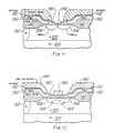
- the third preferred embodiment incorporates additional P++/N Zener diode(s) 474/402 as illustrated in Figure 6 adjacent the DMOS cell array 411, and diode 474/402 has a breakdown voltage slightly less than that of the P++/N diode 464/402 so that breakdown current will first pass through P++ 474 and avoid damage to the DMOS structure.
- the breakdown voltage of a junction diode depends upon the curvature of the junction (the electric field increases as the curvature increases), so the breakdown voltage of diode 464/402 may appear to be the same as that of diode 474/402 because the two P++ regions 464 and 474 are formed by the same process steps.
- D-well 458 covers most of the curved boundary portion of P++ region 464 and lowers the electric field; hence the breakdown voltage of P++ 464/epilayer 402 is higher than that of P++ 474/epilayer 402.
- a typical example would be a breakdown voltage of 75 volts for P++ 464/epilayer 402 compared to 57 volts for P++ 474/epilayer 402.
- Figure 6 also illustrates the source metal 494, gate metal 496, and diode metal 498; field oxide 440, gate oxide 442, D-well 458, source 414, and P ⁇ substrate 401.
- the third preferred embodiment includes source-to-gate diodes in the DMOS by doping the gate Poly 450 during the BASE implant (see step (k) of the first preferred embodiment) about the openings for P++ regions 474 to form concentric P+ rings 473 and 483 and also concentric P+ regions 475 and 485. That is, after the BASE photoresist mask is formed the exposed nitride over Poly is plasma etched away and then the BASE is implanted and diffused. The remaining nitride over Poly is then removed by phosphoric acid revealing the base polysilicon surface which will be doped by the following EMITTER diffusion (see step (l) of the first preferred embodiment). The BASE diffusion oxide grown over the P+ Poly protects the P+ Poly from the emitter dopants. The number of stacked diodes in Poly could be reduced to one or expanded to three or more.
- P++ 474 results in the turn on of the Power DMOS (gate 450 over D-well 458) during voltage transients so that the whole of the silicon area participates in dissipating transient energy.
- drain 404 going to a high voltage yields avalanche conduction into P++ 474 and turns on DMOS gate 450. If the transient drives drain 404 higher due to the inability of the DMOS conductance to discharge the transient, P++ 464 will also avalanche. In this manner both P++ 464 and the DMOS channel participate in dissipating the energy of the transient.
- Poly diode(s) 473/460 plus 483/450 prevent gate to drain forward biasing on application of gate drive voltage under normal drive conditions.
- Zener diodes 450/485 and 462/475 may be incorporated in Poly between gate and source.
- Figure 7 shows the various diodes in the DMOS of the third preferred embodiment. Note that the protection Zener diodes may also be fabricated in silicon 102.
- the fourth preferred embodiment shown in Figure 8 modifies the third preferred embodiment by replacing the P++ 474 with a D-well 574 and P+ contact 575 and using the breakdown of the D-well 574 to N epi 402 lateral diode to dissipate transient energy.
- the breakdown voltage of this diode is adjusted by varying the spacing "l" between D-well 574 and Deep N+ region 432. This permits setting the breakdown voltage less than the D-well 458-P++ 464/epi 402 breakdown voltage.
- the fifth preferred embodiment shown in Figures 6 and 9 further improves SOA performance of the Power DMOS by the use of the buried N+ (DUF 404 in Figure 6 and 104 in Figure 1o) to P substrate (401 in Figure 6 and 102 in Figure 1o) diode which is also optimized to avalanche breakdown in the bulk planar junction at a voltage similar to that of the P++ (474 in Figure 6 and 164 in Figure 1o) to N epi (402 in Figure 6 and 120 in Figure 1o) diode.
- the substrate is tied to ground preferably via the backside of the device through the leadframe to minimize series resistance between the drain and ground.
- the substrate resistivity will be decreased to set the buried N+ to substrate avalanche voltage. Radius of curvature breakdown by the buried N+ is avoided using well known guard ring techniques around the periphery of the buried N+.
- CMOS complementary metal oxide semiconductor field effect transistor
- the present process results in an integrated circuit device having DMOS power transistors for power applications and complementary MOS devices for logic applications.
- the DMOS power structure is more rugged and has a higher power handling capability than prior art DMOS devices due to its self aligned P++ diffusion and, where applied, integral Zener diode.
- Another technical advantage of the present invention is that the process is compatible with the formation of all types of logic components such as TTL, I2L, etc.
- Another advantage of the present process is that any number of desired devices may be included or excluded from the process flow without affecting the overall advantages of the invention. This allows a particular end user to have custom design and application specific circuits fabricated in a mass production process flow.
Landscapes
- Metal-Oxide And Bipolar Metal-Oxide Semiconductor Integrated Circuits (AREA)
- Insulated Gate Type Field-Effect Transistor (AREA)
- Semiconductor Integrated Circuits (AREA)
Applications Claiming Priority (2)
| Application Number | Priority Date | Filing Date | Title |
|---|---|---|---|
| US07/454,811 US5119162A (en) | 1989-02-10 | 1989-12-19 | Integrated power DMOS circuit with protection diode |
| US454811 | 1989-12-19 |
Publications (1)
| Publication Number | Publication Date |
|---|---|
| EP0437939A1 true EP0437939A1 (de) | 1991-07-24 |
Family
ID=23806213
Family Applications (1)
| Application Number | Title | Priority Date | Filing Date |
|---|---|---|---|
| EP90313365A Withdrawn EP0437939A1 (de) | 1989-12-19 | 1990-12-10 | Integrierbarer DMOS-Transistor und Verfahren zu dessen Herstellung |
Country Status (3)
| Country | Link |
|---|---|
| US (1) | US5119162A (de) |
| EP (1) | EP0437939A1 (de) |
| JP (1) | JPH06318707A (de) |
Cited By (13)
| Publication number | Priority date | Publication date | Assignee | Title |
|---|---|---|---|---|
| FR2698486A1 (fr) * | 1992-11-24 | 1994-05-27 | Sgs Thomson Microelectronics | Structure de protection contre les surtensions directes pour composant semiconducteur vertical. |
| EP0621637A1 (de) * | 1993-04-22 | 1994-10-26 | Fuji Electric Co. Ltd. | Schutzdiode für einen Transistor |
| EP0622850A1 (de) * | 1993-04-30 | 1994-11-02 | International Business Machines Corporation | Schutzdiode gegen elektrostatische Entladungen in der Silizium-auf-Insulator-Technologie |
| EP0646964A1 (de) * | 1993-09-30 | 1995-04-05 | Consorzio per la Ricerca sulla Microelettronica nel Mezzogiorno - CoRiMMe | Integrierte aktive Klammerungsstruktur für den Schutz von Leistungsanordnungen gegen Überspannungen, und Verfahren zu ihrer Herstellung |
| EP0657933A1 (de) * | 1993-12-13 | 1995-06-14 | Consorzio per la Ricerca sulla Microelettronica nel Mezzogiorno - CoRiMMe | Integrierte aktive Klammerungsstruktur für den Schutz von Leistungshalbleiterbauelementen gegen Überspannungen |
| NL9500370A (nl) * | 1994-02-24 | 1995-10-02 | Mitsubishi Electric Corp | Halfgeleiderinrichting en werkwijze voor het vervaardigen daarvan. |
| EP0545484A3 (en) * | 1991-12-05 | 1996-11-20 | Cons Ric Microelettronica | Manufacturing process for insulated gate field effect transistors (igfet) with low short circuit density between gate and source and devices obtained thereby |
| EP0747966A3 (de) * | 1995-06-07 | 1997-12-10 | Harris Corporation | Quasi-vertikaler DMOS in MOS- oder BICMOS-Verfahren mit hohem Wirkungsgrad |
| FR2756102A1 (fr) * | 1996-10-25 | 1998-05-22 | Int Rectifier Corp | Dispositif a semi-conducteur commande par une grille mos et procede pour sa fabrication |
| EP0851507A3 (de) * | 1996-12-28 | 1999-05-19 | Samsung Electronics Co., Ltd. | Verfahren zur Herstellung eines DMOS Transistors |
| EP0746033A3 (de) * | 1995-06-02 | 1999-06-02 | Texas Instruments Incorporated | Verbesserungen in der oder in Bezug auf die Halbleiterherstellung |
| EP1119050A1 (de) * | 1992-09-21 | 2001-07-25 | SILICONIX Incorporated | BiCDMOS-Herstellungstechnologie und deren Strukturen |
| US12393214B2 (en) | 2019-06-21 | 2025-08-19 | Wolfspeed, Inc. | Device design for short-circuit protection of transistors |
Families Citing this family (39)
| Publication number | Priority date | Publication date | Assignee | Title |
|---|---|---|---|---|
| US5387811A (en) * | 1991-01-25 | 1995-02-07 | Nec Corporation | Composite semiconductor device with a particular bipolar structure |
| US5481129A (en) * | 1991-10-30 | 1996-01-02 | Harris Corporation | Analog-to-digital converter |
| US5856695A (en) * | 1991-10-30 | 1999-01-05 | Harris Corporation | BiCMOS devices |
| JPH05226589A (ja) * | 1992-02-17 | 1993-09-03 | Mitsubishi Electric Corp | C−BiCMOS型半導体装置およびその製造方法 |
| JP3462886B2 (ja) * | 1993-03-11 | 2003-11-05 | 株式会社東芝 | 半導体装置 |
| DE69326771T2 (de) | 1993-12-07 | 2000-03-02 | Stmicroelectronics S.R.L., Agrate Brianza | Ausgangstufe mit Transistoren von unterschiedlichem Typ |
| EP0681319B1 (de) * | 1994-04-15 | 2002-10-30 | Kabushiki Kaisha Toshiba | Halbleiterbauteil und Verfahren zur Herstellung desselben |
| US6004840A (en) * | 1994-04-15 | 1999-12-21 | Kabushiki Kaisha Toshiba | Method of fabricating a semiconductor device comprising a MOS portion and a bipolar portion |
| FR2725307B1 (fr) * | 1994-09-30 | 1996-12-20 | Sgs Thomson Microelectronics | Composant semiconducteur d'alimentation, de recirculation et de demagnetisation d'une charge selfique |
| JP3400181B2 (ja) * | 1995-04-25 | 2003-04-28 | ローム株式会社 | 半導体装置およびその製造方法 |
| US5578860A (en) * | 1995-05-01 | 1996-11-26 | Motorola, Inc. | Monolithic high frequency integrated circuit structure having a grounded source configuration |
| US6242787B1 (en) | 1995-11-15 | 2001-06-05 | Denso Corporation | Semiconductor device and manufacturing method thereof |
| US6831331B2 (en) | 1995-11-15 | 2004-12-14 | Denso Corporation | Power MOS transistor for absorbing surge current |
| US5578841A (en) * | 1995-12-18 | 1996-11-26 | Motorola, Inc. | Vertical MOSFET device having frontside and backside contacts |
| JP3513609B2 (ja) * | 1996-04-19 | 2004-03-31 | 株式会社ルネサステクノロジ | 半導体装置 |
| US6172383B1 (en) | 1997-12-31 | 2001-01-09 | Siliconix Incorporated | Power MOSFET having voltage-clamped gate |
| US6268242B1 (en) * | 1997-12-31 | 2001-07-31 | Richard K. Williams | Method of forming vertical mosfet device having voltage clamped gate and self-aligned contact |
| JPH11251594A (ja) * | 1997-12-31 | 1999-09-17 | Siliconix Inc | 電圧クランプされたゲ―トを有するパワ―mosfet |
| TW405243B (en) * | 1998-02-25 | 2000-09-11 | Koninkl Philips Electronics Nv | Semiconductor device comprising a mos transistor |
| KR100281908B1 (ko) * | 1998-11-20 | 2001-02-15 | 김덕중 | 반도체소자 및 그 제조방법 |
| JP2000216277A (ja) * | 1999-01-20 | 2000-08-04 | Nec Corp | 半導体装置及びその製造方法 |
| US6614633B1 (en) | 1999-03-19 | 2003-09-02 | Denso Corporation | Semiconductor device including a surge protecting circuit |
| US6365932B1 (en) | 1999-08-20 | 2002-04-02 | Denso Corporation | Power MOS transistor |
| DE19943146C1 (de) * | 1999-09-09 | 2001-01-25 | Infineon Technologies Ag | Brückenschaltung zum Schalten hoher Ströme |
| TW426932B (en) * | 1999-10-04 | 2001-03-21 | Winbond Electronics Corp | Manufacturing method of forming capacitor during formation of BiCMOS device and the device thereof |
| US6855985B2 (en) * | 2002-09-29 | 2005-02-15 | Advanced Analogic Technologies, Inc. | Modular bipolar-CMOS-DMOS analog integrated circuit & power transistor technology |
| US6798022B1 (en) * | 2003-03-11 | 2004-09-28 | Oki Electric Industry Co., Ltd. | Semiconductor device with improved protection from electrostatic discharge |
| US7598573B2 (en) * | 2004-11-16 | 2009-10-06 | Robert Paul Masleid | Systems and methods for voltage distribution via multiple epitaxial layers |
| US7667288B2 (en) * | 2004-11-16 | 2010-02-23 | Masleid Robert P | Systems and methods for voltage distribution via epitaxial layers |
| KR101102966B1 (ko) * | 2004-12-30 | 2012-01-05 | 매그나칩 반도체 유한회사 | 고전압 반도체 소자 및 그 제조 방법 |
| US20070069309A1 (en) * | 2005-09-26 | 2007-03-29 | Richard Lindsay | Buried well for semiconductor devices |
| JP5352062B2 (ja) * | 2007-05-15 | 2013-11-27 | ルネサスエレクトロニクス株式会社 | 静電気保護回路 |
| DE102008062693B4 (de) * | 2008-12-17 | 2017-02-09 | Texas Instruments Deutschland Gmbh | Halbleiterbauelement und Verfahren zu dessen Herstellung |
| KR20130081547A (ko) * | 2012-01-09 | 2013-07-17 | 한국전자통신연구원 | 반도체 소자 및 그 제조 방법 |
| US9929698B2 (en) * | 2013-03-15 | 2018-03-27 | Qualcomm Incorporated | Radio frequency integrated circuit (RFIC) charged-device model (CDM) protection |
| KR102089048B1 (ko) | 2014-02-10 | 2020-03-13 | 한국전자통신연구원 | 반도체 소자 및 그 제조 방법 |
| TWI755334B (zh) * | 2021-01-22 | 2022-02-11 | 立錡科技股份有限公司 | 齊納二極體及其製造方法 |
| CN113451216B (zh) * | 2021-06-28 | 2022-03-25 | 中国电子科技集团公司第二十四研究所 | 成套硅基抗辐射高压cmos器件集成结构及其制造方法 |
| CN121038252B (zh) * | 2025-10-31 | 2026-02-13 | 江苏元感微电子有限公司 | 一种mems散热装置及电子设备 |
Citations (4)
| Publication number | Priority date | Publication date | Assignee | Title |
|---|---|---|---|---|
| EP0071916A2 (de) * | 1981-08-12 | 1983-02-16 | Siemens Aktiengesellschaft | Leistungs-MOS-Feldeffekttransistor und Verfahren zu seiner Herstellung |
| EP0097866A2 (de) * | 1982-06-28 | 1984-01-11 | General Electric Company | Verfahren zum Herstellen einer Halbleiteranordnung mit einem Basisgebiet, das einen tiefen Bereich aufweist |
| EP0292782A2 (de) * | 1987-05-29 | 1988-11-30 | Nissan Motor Co., Ltd. | Vertikaler MOSFET mit einer Spannungsregler-Diode, die sich nicht tief unter der Oberfläche befindet |
| EP0294881A2 (de) * | 1987-06-08 | 1988-12-14 | Philips Electronics Uk Limited | Halbleiteranordnung und Schaltung, geeignet für die Verwendung in intelligenten Leistungsschaltern |
Family Cites Families (6)
| Publication number | Priority date | Publication date | Assignee | Title |
|---|---|---|---|---|
| US4546370A (en) * | 1979-02-15 | 1985-10-08 | Texas Instruments Incorporated | Monolithic integration of logic, control and high voltage interface circuitry |
| JPS5825264A (ja) * | 1981-08-07 | 1983-02-15 | Hitachi Ltd | 絶縁ゲート型半導体装置 |
| JPH0693485B2 (ja) * | 1985-11-29 | 1994-11-16 | 日本電装株式会社 | 半導体装置 |
| JPH0685441B2 (ja) * | 1986-06-18 | 1994-10-26 | 日産自動車株式会社 | 半導体装置 |
| JP2521783B2 (ja) * | 1987-09-28 | 1996-08-07 | 三菱電機株式会社 | 半導体装置およびその製造方法 |
| US4980741A (en) * | 1989-02-10 | 1990-12-25 | General Electric Company | MOS protection device |
-
1989
- 1989-12-19 US US07/454,811 patent/US5119162A/en not_active Expired - Lifetime
-
1990
- 1990-12-10 EP EP90313365A patent/EP0437939A1/de not_active Withdrawn
- 1990-12-19 JP JP2419274A patent/JPH06318707A/ja active Pending
Patent Citations (4)
| Publication number | Priority date | Publication date | Assignee | Title |
|---|---|---|---|---|
| EP0071916A2 (de) * | 1981-08-12 | 1983-02-16 | Siemens Aktiengesellschaft | Leistungs-MOS-Feldeffekttransistor und Verfahren zu seiner Herstellung |
| EP0097866A2 (de) * | 1982-06-28 | 1984-01-11 | General Electric Company | Verfahren zum Herstellen einer Halbleiteranordnung mit einem Basisgebiet, das einen tiefen Bereich aufweist |
| EP0292782A2 (de) * | 1987-05-29 | 1988-11-30 | Nissan Motor Co., Ltd. | Vertikaler MOSFET mit einer Spannungsregler-Diode, die sich nicht tief unter der Oberfläche befindet |
| EP0294881A2 (de) * | 1987-06-08 | 1988-12-14 | Philips Electronics Uk Limited | Halbleiteranordnung und Schaltung, geeignet für die Verwendung in intelligenten Leistungsschaltern |
Non-Patent Citations (1)
| Title |
|---|
| PATENT ABSTRACTS OF JAPAN, vol. 9, no. 310 (E-364)[2033], 6th December 1985; & JP-A-60 144 972 (TOSHIBA K.K.) 31-07-1985 * |
Cited By (20)
| Publication number | Priority date | Publication date | Assignee | Title |
|---|---|---|---|---|
| EP0545484A3 (en) * | 1991-12-05 | 1996-11-20 | Cons Ric Microelettronica | Manufacturing process for insulated gate field effect transistors (igfet) with low short circuit density between gate and source and devices obtained thereby |
| EP1119050A1 (de) * | 1992-09-21 | 2001-07-25 | SILICONIX Incorporated | BiCDMOS-Herstellungstechnologie und deren Strukturen |
| EP0599745A1 (de) * | 1992-11-24 | 1994-06-01 | STMicroelectronics S.A. | Überspannungsschutzstruktur für vertikale Halbleiterkomponenten |
| FR2698486A1 (fr) * | 1992-11-24 | 1994-05-27 | Sgs Thomson Microelectronics | Structure de protection contre les surtensions directes pour composant semiconducteur vertical. |
| EP0621637A1 (de) * | 1993-04-22 | 1994-10-26 | Fuji Electric Co. Ltd. | Schutzdiode für einen Transistor |
| US5561313A (en) * | 1993-04-22 | 1996-10-01 | Fuji Electric Co., Ltd. | Protective diode for transistor |
| EP0622850A1 (de) * | 1993-04-30 | 1994-11-02 | International Business Machines Corporation | Schutzdiode gegen elektrostatische Entladungen in der Silizium-auf-Insulator-Technologie |
| US5654225A (en) * | 1993-09-30 | 1997-08-05 | Consorzio Per La Ricerca Sulla Microelettronica Nel Mezzogiorno | Integrated structure active clamp for the protection of power devices against overvoltages, and manufacturing process thereof |
| EP0646964A1 (de) * | 1993-09-30 | 1995-04-05 | Consorzio per la Ricerca sulla Microelettronica nel Mezzogiorno - CoRiMMe | Integrierte aktive Klammerungsstruktur für den Schutz von Leistungsanordnungen gegen Überspannungen, und Verfahren zu ihrer Herstellung |
| US5777367A (en) * | 1993-09-30 | 1998-07-07 | Consorzio Per La Ricerca Sulla Microelettronica Nel Mezzogiorno | Integrated structure active clamp for the protection of power devices against overvoltages |
| EP0657933A1 (de) * | 1993-12-13 | 1995-06-14 | Consorzio per la Ricerca sulla Microelettronica nel Mezzogiorno - CoRiMMe | Integrierte aktive Klammerungsstruktur für den Schutz von Leistungshalbleiterbauelementen gegen Überspannungen |
| US5530271A (en) * | 1993-12-13 | 1996-06-25 | Consorzio Per La Ricerca Sulla Microelettronica Nel Mezzogiorno | Integrated structure active clamp for the protection of power semiconductor devices against overvoltages |
| NL9500370A (nl) * | 1994-02-24 | 1995-10-02 | Mitsubishi Electric Corp | Halfgeleiderinrichting en werkwijze voor het vervaardigen daarvan. |
| EP0746033A3 (de) * | 1995-06-02 | 1999-06-02 | Texas Instruments Incorporated | Verbesserungen in der oder in Bezug auf die Halbleiterherstellung |
| EP0747966A3 (de) * | 1995-06-07 | 1997-12-10 | Harris Corporation | Quasi-vertikaler DMOS in MOS- oder BICMOS-Verfahren mit hohem Wirkungsgrad |
| FR2756102A1 (fr) * | 1996-10-25 | 1998-05-22 | Int Rectifier Corp | Dispositif a semi-conducteur commande par une grille mos et procede pour sa fabrication |
| US6043126A (en) * | 1996-10-25 | 2000-03-28 | International Rectifier Corporation | Process for manufacture of MOS gated device with self aligned cells |
| US6144065A (en) * | 1996-10-25 | 2000-11-07 | International Rectifier Corporation | MOS gated device with self aligned cells |
| EP0851507A3 (de) * | 1996-12-28 | 1999-05-19 | Samsung Electronics Co., Ltd. | Verfahren zur Herstellung eines DMOS Transistors |
| US12393214B2 (en) | 2019-06-21 | 2025-08-19 | Wolfspeed, Inc. | Device design for short-circuit protection of transistors |
Also Published As
| Publication number | Publication date |
|---|---|
| JPH06318707A (ja) | 1994-11-15 |
| US5119162A (en) | 1992-06-02 |
Similar Documents
| Publication | Publication Date | Title |
|---|---|---|
| US5119162A (en) | Integrated power DMOS circuit with protection diode | |
| US5102809A (en) | SOI BICMOS process | |
| US5171699A (en) | Vertical DMOS transistor structure built in an N-well CMOS-based BiCMOS process and method of fabrication | |
| US5034337A (en) | Method of making an integrated circuit that combines multi-epitaxial power transistors with logic/analog devices | |
| US6902967B2 (en) | Integrated circuit with a MOS structure having reduced parasitic bipolar transistor action | |
| KR100200059B1 (ko) | 쇼트키 장벽 다이오드 및 쇼트키 장벽 다이오드 클램프형 트랜지스터와 이들을 제조하는 방법 | |
| EP0097379B1 (de) | Verfahren zum Herstellen von Halbleiteranordnungen | |
| US5424572A (en) | Spacer formation in a semiconductor structure | |
| KR100223098B1 (ko) | Bicmos 디바이스 및 그 제조방법 | |
| US5382538A (en) | Method for forming MOS transistors having vertical current flow and resulting structure | |
| US5679587A (en) | Method of fabricating an integrated circuit with vertical bipolar power transistors and isolated lateral bipolar control transistors | |
| JPH0744232B2 (ja) | Bi―CMOSデバイス製造方法 | |
| US5256582A (en) | Method of forming complementary bipolar and MOS transistor having power and logic structures on the same integrated circuit substrate | |
| US6215160B1 (en) | Semiconductor device having bipolar transistor and field effect transistor and method of manufacturing the same | |
| US4962053A (en) | Bipolar transistor fabrication utilizing CMOS techniques | |
| EP0158292B1 (de) | Halbleiteranordnung mit einem Treiberschaltungselement und einem Ausgangstransistor | |
| KR100199465B1 (ko) | 반도체 디바이스용으로 제조되는 접점구조물 및 이를 제조하는 방법 | |
| KR910006672B1 (ko) | 반도체 집적회로 장치 및 그의 제조 방법 | |
| US5049513A (en) | Bi CMOS/SOI process flow | |
| EP0233202B1 (de) | Herstellung einer halbleitervorrichtung mit eingebettetem oxyd | |
| KR0128339B1 (ko) | Cmos 기술을 이용하는 바이폴라 트랜지스터 제조방법 | |
| JPH08186259A (ja) | 3端子電力絶縁ゲートトランジスタ及びその製造方法 | |
| US5181095A (en) | Complementary bipolar and MOS transistor having power and logic structures on the same integrated circuit substrate | |
| US5624856A (en) | Method for forming a lateral bipolar transistor | |
| US5153697A (en) | Integrated circuit that combines multi-epitaxial power transistors with logic/analog devices, and a process to produce same |
Legal Events
| Date | Code | Title | Description |
|---|---|---|---|
| PUAI | Public reference made under article 153(3) epc to a published international application that has entered the european phase |
Free format text: ORIGINAL CODE: 0009012 |
|
| AK | Designated contracting states |
Kind code of ref document: A1 Designated state(s): DE FR GB IT NL |
|
| 17P | Request for examination filed |
Effective date: 19920108 |
|
| 17Q | First examination report despatched |
Effective date: 19931108 |
|
| STAA | Information on the status of an ep patent application or granted ep patent |
Free format text: STATUS: THE APPLICATION IS DEEMED TO BE WITHDRAWN |
|
| 18D | Application deemed to be withdrawn |
Effective date: 19940519 |