EP0599745A1 - Überspannungsschutzstruktur für vertikale Halbleiterkomponenten - Google Patents
Überspannungsschutzstruktur für vertikale Halbleiterkomponenten Download PDFInfo
- Publication number
- EP0599745A1 EP0599745A1 EP93420458A EP93420458A EP0599745A1 EP 0599745 A1 EP0599745 A1 EP 0599745A1 EP 93420458 A EP93420458 A EP 93420458A EP 93420458 A EP93420458 A EP 93420458A EP 0599745 A1 EP0599745 A1 EP 0599745A1
- Authority
- EP
- European Patent Office
- Prior art keywords
- cells
- power transistor
- transistor
- type
- main electrode
- Prior art date
- Legal status (The legal status is an assumption and is not a legal conclusion. Google has not performed a legal analysis and makes no representation as to the accuracy of the status listed.)
- Granted
Links
Images
Classifications
-
- H—ELECTRICITY
- H10—SEMICONDUCTOR DEVICES; ELECTRIC SOLID-STATE DEVICES NOT OTHERWISE PROVIDED FOR
- H10D—INORGANIC ELECTRIC SEMICONDUCTOR DEVICES
- H10D30/00—Field-effect transistors [FET]
- H10D30/60—Insulated-gate field-effect transistors [IGFET]
- H10D30/64—Double-diffused metal-oxide semiconductor [DMOS] FETs
- H10D30/66—Vertical DMOS [VDMOS] FETs
-
- H—ELECTRICITY
- H10—SEMICONDUCTOR DEVICES; ELECTRIC SOLID-STATE DEVICES NOT OTHERWISE PROVIDED FOR
- H10D—INORGANIC ELECTRIC SEMICONDUCTOR DEVICES
- H10D84/00—Integrated devices formed in or on semiconductor substrates that comprise only semiconducting layers, e.g. on Si wafers or on GaAs-on-Si wafers
- H10D84/101—Integrated devices comprising main components and built-in components, e.g. IGBT having built-in freewheel diode
- H10D84/141—VDMOS having built-in components
- H10D84/148—VDMOS having built-in components the built-in components being breakdown diodes, e.g. Zener diodes
-
- H—ELECTRICITY
- H10—SEMICONDUCTOR DEVICES; ELECTRIC SOLID-STATE DEVICES NOT OTHERWISE PROVIDED FOR
- H10D—INORGANIC ELECTRIC SEMICONDUCTOR DEVICES
- H10D89/00—Aspects of integrated devices not covered by groups H10D84/00 - H10D88/00
- H10D89/60—Integrated devices comprising arrangements for electrical or thermal protection, e.g. protection circuits against electrostatic discharge [ESD]
-
- H—ELECTRICITY
- H10—SEMICONDUCTOR DEVICES; ELECTRIC SOLID-STATE DEVICES NOT OTHERWISE PROVIDED FOR
- H10D—INORGANIC ELECTRIC SEMICONDUCTOR DEVICES
- H10D89/00—Aspects of integrated devices not covered by groups H10D84/00 - H10D88/00
- H10D89/60—Integrated devices comprising arrangements for electrical or thermal protection, e.g. protection circuits against electrostatic discharge [ESD]
- H10D89/601—Integrated devices comprising arrangements for electrical or thermal protection, e.g. protection circuits against electrostatic discharge [ESD] for devices having insulated gate electrodes, e.g. for IGFETs or IGBTs
-
- H—ELECTRICITY
- H10—SEMICONDUCTOR DEVICES; ELECTRIC SOLID-STATE DEVICES NOT OTHERWISE PROVIDED FOR
- H10D—INORGANIC ELECTRIC SEMICONDUCTOR DEVICES
- H10D89/00—Aspects of integrated devices not covered by groups H10D84/00 - H10D88/00
- H10D89/60—Integrated devices comprising arrangements for electrical or thermal protection, e.g. protection circuits against electrostatic discharge [ESD]
- H10D89/601—Integrated devices comprising arrangements for electrical or thermal protection, e.g. protection circuits against electrostatic discharge [ESD] for devices having insulated gate electrodes, e.g. for IGFETs or IGBTs
- H10D89/611—Integrated devices comprising arrangements for electrical or thermal protection, e.g. protection circuits against electrostatic discharge [ESD] for devices having insulated gate electrodes, e.g. for IGFETs or IGBTs using diodes as protective elements
-
- H—ELECTRICITY
- H10—SEMICONDUCTOR DEVICES; ELECTRIC SOLID-STATE DEVICES NOT OTHERWISE PROVIDED FOR
- H10D—INORGANIC ELECTRIC SEMICONDUCTOR DEVICES
- H10D84/00—Integrated devices formed in or on semiconductor substrates that comprise only semiconducting layers, e.g. on Si wafers or on GaAs-on-Si wafers
- H10D84/101—Integrated devices comprising main components and built-in components, e.g. IGBT having built-in freewheel diode
- H10D84/141—VDMOS having built-in components
Definitions
- the present invention relates to high voltage vertical power transistors which are devices made vertically in a silicon wafer, the rear face of which is connected to a high voltage.
- the invention applies to vertical power transistors of the MOS or bipolar type with insulated gate. It applies in particular to “smart power switches” which are circuits comprising vertical power components and logic control circuits for these components on the same silicon chip.
- Power transistors are designed to withstand a defined forward voltage (for example 400 volts). If the external circuit applies a higher voltage to the device, the latter enters a breakdown mode liable to damage it. For example, switching an inductive load produces an overvoltage with a certain amount of energy to be dissipated. This overvoltage is applied to the power switch which is in the blocked state or in a transient phase of transition to the blocked state.
- One of the solutions for protecting the transistor consists in sending a signal to its control electrode to bring it briefly into a conductive state for the time necessary to drain the excessive energy.
- MOS type power transistors In what follows, reference will always be made to MOS type power transistors. However, it will be clear that everything stated about these transistors also applies to insulated gate bipolar transistors (IGBT) which are structurally substantially identical except for the fact that they include on the side of their face. rear a layer of conductivity type opposite to that of the layer constituting the rear face of a power MOS transistor.
- IGBT insulated gate bipolar transistors
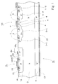
- FIG. 1 shows in section an example of a conventional mixed structure comprising a vertical power MOS transistor TP of the diffused type (VDMOS), two cells of which are represented, this transistor being associated with logic circuits of which an N channel MOS transistor TL is illustrated.
- the vertical MOS transistor is made up of a large number of identical cells in parallel, for example 10,000.
- a cell of the power MOS transistor TP comprises a well 1 (1-1, 1-2) consisting of a diffusion of the type P.
- an annular diffusion 2 of type N+ is produced which constitutes an element of the source of the power transistor.
- the diffusions 2 are connected together by a conductive layer 3 which is for example made of aluminum.
- the surface peripheral areas of regions 1 constitute a channel region 4 of the power transistor.
- each box 1 generally comprises a deeper and more doped central part 5 (5-1, 5-2).
- Each cell of the power MOS transistor TP comprises a gate 6 formed by a layer of polycrystalline silicon. This grid 6 is separated from the substrate 1 by an oxide layer 7. All the grids 6 are interconnected.
- the rear face 10 of the substrate 1 comprises an overdoped layer 11 coated with a drain metallization 12.
- the MOS transistor TL of the logic part is formed in a P-type well 14.
- This well 14 has two diffused zones of N+ type, the first constituting the source 15 and the second constituting the drain 16 of the TL transistor.
- This transistor comprises a gate 18 formed by a layer of polycrystalline silicon.
- the grid 18 is separated from the box 14 by an oxide layer 19.
- the diffused zones constituting the source 15 and the drain 16 are each connected to a conductive line designated by 20, 21, respectively.
- the conductive lines 20, 21 are for example made of aluminum.
- a zone 23 of the P+ type is provided in the box 14 connected to a conductive layer 24.
- the zone 23 and the conductive layer 24 allow the box 14 to be grounded.
- the rear face metallization 12 is connected to a positive potential and the front face metallizations 3 of the power transistor are connected to a negative potential with respect to this positive potential, for example a potential close to the ground potential. .
- the problem that we want to solve is to avoid the conduction by breakdown of the power transistor, that is to say the junction between the substrate 0 and the wells P (1-1, 5-1; 1-2, 5-2) when the drain voltage increases while the transistor is in the off state.
- This conduction is undesirable because it can cause heating of the area where the avalanche is created due to an excessive current flow and this heating can be destructive.
- the structure is designed so that this last junction slams after that of the cells of the power transistors.
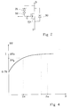
- An avalanche diode having a triggering threshold lower than that of the cells of the power MOS transistor can be used in a conventional manner, for example as illustrated in FIG. 2 where the power transistor TP is represented with its drain terminals D, source S and gate G. This transistor comprises a reverse conduction diode 30.
- An avalanche diode 31 can be connected between the drain and the gate with preferably the interposition of a direct diode series 32 to avoid any derivation of normal signals control panel.
- the circuit of FIG. 2 is only shown by way of example because many other arrangements for triggering a main transistor after triggering a detection avalanche diode are known. It will be noted that, in most of these arrangements, as illustrated in FIG. 2, the cathode of the avalanche diode is connected to the drain of the power transistor. This cathode or this drain corresponds to the common terminal 12 of FIG. 1.
- an object of the present invention is to provide in a vertical type power transistor, a structure for protection against direct overvoltages which can be produced in a semiconductor wafer containing a power semiconductor component without requiring a modification of the structure ( of the drawing) of the cells of the power transistor.
- Another object of the present invention is to provide such a protection structure whose trigger threshold is determined with precision relative to the trigger threshold in avalanche of the cells of the power transistor.
- Another object of the present invention is to provide such a protective structure which can be produced without modifying the method of manufacturing the component comprising one or more power transistors and possibly a logic control circuit.
- the present invention provides a vertical power transistor of the MOS or IGBT type, the rear face of which constitutes a first main electrode and the front face of which comprises a large number of identical cells connected in parallel to a second main electrode and to a control electrode, this transistor further comprising at least one additional cell formed in the front face with the same shape but with smaller lateral dimensions than said identical cells, and means for switching on the power transistor when the additional cell enters an avalanche.
- the present invention provides a vertical power transistor of the MOS or IGBT type consisting of a plurality of identical active cells, each of which comprises on the side of the upper face of a substrate of a first type of conductivity a well of the second type of conductivity with a low doping level, the central part of which is deeper and more doped, a substantially peripheral and upper region of each well having a high level of doping of the first type of conductivity, a first main electrode being in contact with the upper surface of the central region and of the peripheral region, a control electrode being arranged, with the interposition of an insulating layer, above the periphery of each box, a second main electrode being formed on the underside of the substrate, this transistor comprising at least one additional cell manufactured according to the same steps t echnological than the active cells and arranged among them, each additional cell being of smaller lateral dimensions, at least as regards its deeper and more doped part than the other cells and its first main electrode being connected to a control circuit for switching on the power transistor.
- the cells of the power transistor are arranged in rows and columns and the additional cells are arranged in a row placed among the rows of cells of the power transistor.
- the protection structure according to the present invention uses as a detector element a cell identical to those of the power transistor, but only of smaller dimension, the triggering threshold of this cell is determined in a reliable and reproducible manner with respect to the threshold for triggering a direct avalanche of the cells of the power transistor.
- the drift will be identical for the detection cells and for the cells of the power transistor and the trigger threshold difference will remain substantially the same.
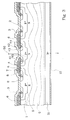
- FIG. 3 represents a partial section view of a power MOS transistor of the VDMOS type including an overvoltage detector element according to the present invention.
- the cells of the power transistor are formed in a substrate 0, the rear face of which comprises a region N+ 11 and is coated with a metallization 12 which will correspond to the drain metallization of the MOS transistor.
- P type 1 comprising a central zone 5 Pd type overdoped.
- Source diffusions 2 of annular shape are formed in each box and laterally delimit a channel zone 4 surmounted by a grid region 6, with interposition an insulating layer 7, commonly an oxide layer.
- a layer of an insulator, for example of silicon oxide 8, has been shown surrounding the grid 6 to isolate this grid from the source metallization 3.
- This source metallization 3 is, as indicated above, in contact on the one hand with the central upper surface of the box 1, on the other hand with the regions 2 of type N+.
- the present invention provides for adding to such a structure at least one additional cell whose elements 41 to 48 respectively correspond to elements 1 to 8 of the cell of a power MOS transistor.
- the only difference is that all the elements of the additional cell are reduced in lateral dimensions compared to the elements of the cell of the power MOS transistor.
- the appearance of the equipotential lines existing in the substrate 0 is also shown in dotted lines when the drain 12 is subjected to a relatively high potential compared to the source metallizations 3, while the component is not put in the conducting state. , this relatively high voltage being lower than the breakdown voltage between the region N of the substrate and the regions P+ of the various cells. Note that, due to the smaller size of the additional cells, the curvature of the field lines is more pronounced in the vicinity of these cells. As a result, in a manner known to those skilled in the art, when the drain potential continues to increase relative to the source potential, the breakdown will take place first at the locations where the field lines are most curved, that is to say at the level of the additional cells of smaller dimension. Thus, these additional cells of smaller size have thus constituted a detection diode which will slam slightly before the cells of the power transistor.
- the additional cells have exactly the same shape but only a smaller dimension than the cells of the power transistor, the difference between the breakdown voltages of these additional cells and of the cells of the power transistor is well determined and depends only on the dimensional relationship between the additional cells and the cells of the power transistor.
- additional detection cells of the type of that illustrated in FIG. 3.
- the position of these cells with respect to the cells of the power transistor being chosen by the designer of the circuit to minimize the differences between a conventional component and a component according to the present invention including additional detection diodes.
- the additional cells could for example constitute a row of cells interspersed among the many rows of cells of the power component. All the metallizations 43 of the additional cells are connected to the same terminal 50 and the additional diodes according to the present invention will, for example, be connected in an arrangement of the type of that of FIG. 2 so that, after the appearance of an overvoltage which has caused a breakdown of the additional diodes, cause the power transistor TP to be momentarily turned on.
- the present invention is susceptible of numerous variants and modifications which will appear to those skilled in the art, in particular as regards the number and arrangement of the additional cells according to the present invention and the use of the detection diodes constituted by these cells in a circuit for turning on a main transistor which may be, as indicated above, a VDMOS type transistor, a bipolar insulated gate transistor (IGBT) or any analogous component in its operation and structure.
- a main transistor which may be, as indicated above, a VDMOS type transistor, a bipolar insulated gate transistor (IGBT) or any analogous component in its operation and structure.
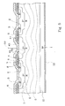
- the zones N+ 42 of the additional cells could be deleted since, in these additional cells, these zones have no functional role.
- FIG. 5 shows, similarly to FIG. 3, an embodiment of the invention in which these zones 42 have been deleted in the additional cells.
Landscapes
- Metal-Oxide And Bipolar Metal-Oxide Semiconductor Integrated Circuits (AREA)
- Insulated Gate Type Field-Effect Transistor (AREA)
- Semiconductor Integrated Circuits (AREA)
Applications Claiming Priority (2)
| Application Number | Priority Date | Filing Date | Title |
|---|---|---|---|
| FR9214478 | 1992-11-24 | ||
| FR9214478A FR2698486B1 (fr) | 1992-11-24 | 1992-11-24 | Structure de protection contre les surtensions directes pour composant semiconducteur vertical. |
Publications (2)
| Publication Number | Publication Date |
|---|---|
| EP0599745A1 true EP0599745A1 (de) | 1994-06-01 |
| EP0599745B1 EP0599745B1 (de) | 2001-07-18 |
Family
ID=9436115
Family Applications (1)
| Application Number | Title | Priority Date | Filing Date |
|---|---|---|---|
| EP93420458A Expired - Lifetime EP0599745B1 (de) | 1992-11-24 | 1993-11-19 | Überspannungsschutzstruktur für vertikale Halbleiterkomponenten |
Country Status (5)
| Country | Link |
|---|---|
| US (3) | US5543645A (de) |
| EP (1) | EP0599745B1 (de) |
| JP (1) | JP3418436B2 (de) |
| DE (1) | DE69330455T2 (de) |
| FR (1) | FR2698486B1 (de) |
Cited By (1)
| Publication number | Priority date | Publication date | Assignee | Title |
|---|---|---|---|---|
| EP0621637A1 (de) * | 1993-04-22 | 1994-10-26 | Fuji Electric Co. Ltd. | Schutzdiode für einen Transistor |
Families Citing this family (25)
| Publication number | Priority date | Publication date | Assignee | Title |
|---|---|---|---|---|
| FR2698486B1 (fr) * | 1992-11-24 | 1995-03-10 | Sgs Thomson Microelectronics | Structure de protection contre les surtensions directes pour composant semiconducteur vertical. |
| EP0696054B1 (de) * | 1994-07-04 | 2002-02-20 | STMicroelectronics S.r.l. | Verfahren zur Herstellung von Leistungsbauteilen hoher Dichte in MOS-Technologie |
| US5798554A (en) * | 1995-02-24 | 1998-08-25 | Consorzio Per La Ricerca Sulla Microelettronica Nel Mezzogiorno | MOS-technology power device integrated structure and manufacturing process thereof |
| US5847429A (en) * | 1995-07-31 | 1998-12-08 | Integrated Device Technology, Inc. | Multiple node ESD devices |
| DE69531783T2 (de) * | 1995-10-09 | 2004-07-15 | Consorzio Per La Ricerca Sulla Microelettronica Nel Mezzogiorno - Corimme | Herstellungsverfahren für Leistungsanordnung mit Schutzring |
| EP0772242B1 (de) | 1995-10-30 | 2006-04-05 | STMicroelectronics S.r.l. | Leistungsbauteil in MOS-Technologie mit einer einzelnen kritischen Grösse |
| EP0772241B1 (de) * | 1995-10-30 | 2004-06-09 | STMicroelectronics S.r.l. | Leistungsbauteil hoher Dichte in MOS-Technologie |
| US6228719B1 (en) | 1995-11-06 | 2001-05-08 | Stmicroelectronics S.R.L. | MOS technology power device with low output resistance and low capacitance, and related manufacturing process |
| DE69518653T2 (de) * | 1995-12-28 | 2001-04-19 | Consorzio Per La Ricerca Sulla Microelettronica Nel Mezzogiorno, Catania | MOS-Technologie-Leistungsanordnung in integrierter Struktur |
| US5913130A (en) * | 1996-06-12 | 1999-06-15 | Harris Corporation | Method for fabricating a power device |
| US5811338A (en) * | 1996-08-09 | 1998-09-22 | Micron Technology, Inc. | Method of making an asymmetric transistor |
| FR2764136B1 (fr) * | 1997-05-28 | 1999-08-13 | Sgs Thomson Microelectronics | Protection contre des surtensions d'un transistor mos de puissance integre |
| US6781804B1 (en) | 1997-06-17 | 2004-08-24 | Sgs-Thomson Microelectronics S.A. | Protection of the logic well of a component including an integrated MOS power transistor |
| FR2764735B1 (fr) * | 1997-06-17 | 1999-08-27 | Sgs Thomson Microelectronics | Protection du caisson logique d'un composant incluant un transistor mos de puissance integre |
| EP0961325B1 (de) | 1998-05-26 | 2008-05-07 | STMicroelectronics S.r.l. | MOS-Technologie-Leistungsanordnung mit hoher Integrationsdichte |
| FR2791193B1 (fr) * | 1999-03-16 | 2004-07-09 | St Microelectronics Sa | Procede de controle du fonctionnement d'une pompe de charge capacitive et dispositif de pompe de charge capacitive correspondant |
| DE19918028A1 (de) * | 1999-04-21 | 2000-11-02 | Siemens Ag | Halbleiter-Bauelement |
| JP2001267431A (ja) * | 2000-03-17 | 2001-09-28 | Nec Corp | 半導体集積回路装置及びその製造方法 |
| US7708751B2 (en) | 2004-05-21 | 2010-05-04 | Ethicon Endo-Surgery, Inc. | MRI biopsy device |
| US8932233B2 (en) | 2004-05-21 | 2015-01-13 | Devicor Medical Products, Inc. | MRI biopsy device |
| US9638770B2 (en) | 2004-05-21 | 2017-05-02 | Devicor Medical Products, Inc. | MRI biopsy apparatus incorporating an imageable penetrating portion |
| ATE440381T1 (de) * | 2005-01-07 | 2009-09-15 | Ami Semiconductor Belgium Bvba | Hybride esd-klemme |
| US7317204B2 (en) * | 2005-01-13 | 2008-01-08 | Samsung Electronics Co., Ltd. | Test structure of semiconductor device |
| DE102006047243A1 (de) | 2006-05-15 | 2007-11-22 | Infineon Technologies Ag | Bordnetz mit mindestens einem Leistungstransistor und Verfahren zum Schutz eines Bordnetzes |
| US8093713B2 (en) * | 2007-02-09 | 2012-01-10 | Infineon Technologies Ag | Module with silicon-based layer |
Citations (5)
| Publication number | Priority date | Publication date | Assignee | Title |
|---|---|---|---|---|
| DE3540433A1 (de) * | 1984-11-20 | 1986-05-22 | Mitsubishi Denki K.K., Tokio/Tokyo | Integriertes mosfet-bauelement |
| JPH02128474A (ja) * | 1988-11-08 | 1990-05-16 | Nec Corp | 電界効果トランジスタ |
| EP0409746A1 (de) * | 1989-07-17 | 1991-01-23 | STMicroelectronics S.A. | Integrierter VDMOS/Logikschaltkreis mit vertikalem Transistor vom Verarmungstyp und einer Zenerdiode |
| EP0416805A2 (de) * | 1989-08-30 | 1991-03-13 | Siliconix, Inc. | Transistor mit Spannungsbegrenzungsanordnung |
| EP0437939A1 (de) * | 1989-12-19 | 1991-07-24 | Texas Instruments Incorporated | Integrierbarer DMOS-Transistor und Verfahren zu dessen Herstellung |
Family Cites Families (18)
| Publication number | Priority date | Publication date | Assignee | Title |
|---|---|---|---|---|
| JPS54112179A (en) * | 1978-02-23 | 1979-09-01 | Sony Corp | Semiconductor device |
| JPS61137368A (ja) * | 1984-12-10 | 1986-06-25 | Hitachi Ltd | 半導体装置 |
| JPS61296770A (ja) * | 1985-06-25 | 1986-12-27 | Nec Corp | 絶縁ゲ−ト電界効果型半導体装置 |
| JPS62144357A (ja) * | 1985-12-19 | 1987-06-27 | Fuji Electric Co Ltd | スイツチング用半導体装置 |
| JPH0685441B2 (ja) * | 1986-06-18 | 1994-10-26 | 日産自動車株式会社 | 半導体装置 |
| IT1213411B (it) * | 1986-12-17 | 1989-12-20 | Sgs Microelettronica Spa | Struttura mos di potenza con dispositivo di protezione contro le sovratensioni e processo per lasua fabbricazione. |
| JP2508826B2 (ja) * | 1987-11-24 | 1996-06-19 | 日本電気株式会社 | 半導体装置 |
| JPH0397269A (ja) * | 1989-09-11 | 1991-04-23 | Fuji Electric Co Ltd | 電流制限回路を内蔵する伝導度変調型mosfet |
| JPH03105977A (ja) * | 1989-09-20 | 1991-05-02 | Hitachi Ltd | 半導体装置 |
| JPH03156977A (ja) * | 1989-11-15 | 1991-07-04 | Sanyo Electric Co Ltd | 縦型mosfet |
| JPH03229469A (ja) * | 1990-02-05 | 1991-10-11 | Matsushita Electron Corp | 縦型mos電界効果トランジスタ |
| JP2692350B2 (ja) * | 1990-04-02 | 1997-12-17 | 富士電機株式会社 | Mos型半導体素子 |
| JPH04132266A (ja) * | 1990-09-21 | 1992-05-06 | Fuji Electric Co Ltd | 半導体装置 |
| JP3064457B2 (ja) * | 1991-03-08 | 2000-07-12 | 関西日本電気株式会社 | スイッチ回路およびゲート電圧クランプ型半導体装置 |
| GB2257830B (en) * | 1991-07-12 | 1995-04-05 | Matsushita Electric Works Ltd | Low output-capacity, double-diffused field effect transistor |
| JP3111576B2 (ja) * | 1992-01-06 | 2000-11-27 | 富士電機株式会社 | 半導体装置 |
| GB9207849D0 (en) | 1992-04-09 | 1992-05-27 | Philips Electronics Uk Ltd | A semiconductor device |
| FR2698486B1 (fr) * | 1992-11-24 | 1995-03-10 | Sgs Thomson Microelectronics | Structure de protection contre les surtensions directes pour composant semiconducteur vertical. |
-
1992
- 1992-11-24 FR FR9214478A patent/FR2698486B1/fr not_active Expired - Fee Related
-
1993
- 1993-11-19 JP JP29030093A patent/JP3418436B2/ja not_active Expired - Fee Related
- 1993-11-19 DE DE69330455T patent/DE69330455T2/de not_active Expired - Fee Related
- 1993-11-19 EP EP93420458A patent/EP0599745B1/de not_active Expired - Lifetime
- 1993-11-23 US US08/157,362 patent/US5543645A/en not_active Expired - Lifetime
-
1995
- 1995-06-07 US US08/479,511 patent/US5563436A/en not_active Expired - Lifetime
- 1995-12-15 US US08/573,300 patent/US5780895A/en not_active Expired - Lifetime
Patent Citations (5)
| Publication number | Priority date | Publication date | Assignee | Title |
|---|---|---|---|---|
| DE3540433A1 (de) * | 1984-11-20 | 1986-05-22 | Mitsubishi Denki K.K., Tokio/Tokyo | Integriertes mosfet-bauelement |
| JPH02128474A (ja) * | 1988-11-08 | 1990-05-16 | Nec Corp | 電界効果トランジスタ |
| EP0409746A1 (de) * | 1989-07-17 | 1991-01-23 | STMicroelectronics S.A. | Integrierter VDMOS/Logikschaltkreis mit vertikalem Transistor vom Verarmungstyp und einer Zenerdiode |
| EP0416805A2 (de) * | 1989-08-30 | 1991-03-13 | Siliconix, Inc. | Transistor mit Spannungsbegrenzungsanordnung |
| EP0437939A1 (de) * | 1989-12-19 | 1991-07-24 | Texas Instruments Incorporated | Integrierbarer DMOS-Transistor und Verfahren zu dessen Herstellung |
Non-Patent Citations (1)
| Title |
|---|
| PATENT ABSTRACTS OF JAPAN vol. 14, no. 362 (E - 960) 6 August 1990 (1990-08-06) * |
Cited By (2)
| Publication number | Priority date | Publication date | Assignee | Title |
|---|---|---|---|---|
| EP0621637A1 (de) * | 1993-04-22 | 1994-10-26 | Fuji Electric Co. Ltd. | Schutzdiode für einen Transistor |
| US5561313A (en) * | 1993-04-22 | 1996-10-01 | Fuji Electric Co., Ltd. | Protective diode for transistor |
Also Published As
| Publication number | Publication date |
|---|---|
| US5780895A (en) | 1998-07-14 |
| DE69330455T2 (de) | 2002-04-18 |
| FR2698486B1 (fr) | 1995-03-10 |
| US5543645A (en) | 1996-08-06 |
| JP3418436B2 (ja) | 2003-06-23 |
| FR2698486A1 (fr) | 1994-05-27 |
| JPH06224436A (ja) | 1994-08-12 |
| US5563436A (en) | 1996-10-08 |
| EP0599745B1 (de) | 2001-07-18 |
| DE69330455D1 (de) | 2001-08-23 |
Similar Documents
| Publication | Publication Date | Title |
|---|---|---|
| EP0599745B1 (de) | Überspannungsschutzstruktur für vertikale Halbleiterkomponenten | |
| EP0409746B1 (de) | Integrierter VDMOS/Logikschaltkreis mit vertikalem Transistor vom Verarmungstyp und einer Zenerdiode | |
| EP0543742B1 (de) | Monolithische Niederspannungsschutzdiode mit geringer Kapazität | |
| EP0388329B1 (de) | Steuerschaltung für einen MOS-Leistungstransistor mit induktiver Last | |
| US3934159A (en) | Semiconductor circuit devices using insulated gate-type field effect elements having protective diodes | |
| EP0963608B1 (de) | Schaltungsanordnung zum schutz von teilnehmerschnittstellen | |
| EP2246885A1 (de) | Schutzvorrichtung für einen integrierten Schaltkreis gegen elektrostatische Entladungen | |
| EP0359680B1 (de) | Integrierbare, aktive Diode | |
| FR2993401A1 (fr) | Transistor mos sur soi protege contre des surtensions | |
| EP0780952A1 (de) | Monolithischer und statischer Strombegrenzer und Schutzschalter | |
| FR2969825A1 (fr) | Composant vertical bidirectionnel a double sillonnage | |
| FR2723259A1 (fr) | Thyristor a commande par mos ayant des caracteristiques de saturation de courant | |
| EP1544919B1 (de) | Triac | |
| FR2719158A1 (fr) | Circuit d'entrée pour protéger un circuit intégré monolithe. | |
| EP0577531B1 (de) | Schutzdiode für ein vertikales Halbleiterbauelement | |
| EP0881681B1 (de) | Anordnung zum Schützen einer integrierten MOS-Vorrichtung gegen Spannungsabfälle | |
| EP0704903B1 (de) | Halbleitervorrichtung zur Speisung, Rückleitung und Entmagnetisierung einer induktiven Last | |
| EP0568466B1 (de) | Vergrabener Lawinendiode | |
| EP0820135B1 (de) | Statischer selbsthaltender Mikroschalter | |
| FR2764735A1 (fr) | Protection du caisson logique d'un composant incluant un transistor mos de puissance integre | |
| EP0462029B1 (de) | Herstellungsverfahren eines Bipolartransistors, der umgekehrten Vorspannungen standhält | |
| EP2246886A1 (de) | Integrierter Schaltkreis, der mit einem großflächigen Schutz gegen elektrostatische Entladungen ausgestattet ist | |
| FR2982077A1 (fr) | Triac a amplification de gachette | |
| GB1422465A (en) | Semiconductor device | |
| EP0929140B1 (de) | Schutz eines vertikalen, Messzellen zugeordneten MOS-Transistors |
Legal Events
| Date | Code | Title | Description |
|---|---|---|---|
| PUAI | Public reference made under article 153(3) epc to a published international application that has entered the european phase |
Free format text: ORIGINAL CODE: 0009012 |
|
| AK | Designated contracting states |
Kind code of ref document: A1 Designated state(s): DE FR GB IT |
|
| 17P | Request for examination filed |
Effective date: 19941109 |
|
| 17Q | First examination report despatched |
Effective date: 19980805 |
|
| RAP3 | Party data changed (applicant data changed or rights of an application transferred) |
Owner name: STMICROELECTRONICS S.A. |
|
| GRAG | Despatch of communication of intention to grant |
Free format text: ORIGINAL CODE: EPIDOS AGRA |
|
| GRAG | Despatch of communication of intention to grant |
Free format text: ORIGINAL CODE: EPIDOS AGRA |
|
| GRAH | Despatch of communication of intention to grant a patent |
Free format text: ORIGINAL CODE: EPIDOS IGRA |
|
| GRAH | Despatch of communication of intention to grant a patent |
Free format text: ORIGINAL CODE: EPIDOS IGRA |
|
| GRAA | (expected) grant |
Free format text: ORIGINAL CODE: 0009210 |
|
| AK | Designated contracting states |
Kind code of ref document: B1 Designated state(s): DE FR GB IT |
|
| PG25 | Lapsed in a contracting state [announced via postgrant information from national office to epo] |
Ref country code: IT Free format text: LAPSE BECAUSE OF FAILURE TO SUBMIT A TRANSLATION OF THE DESCRIPTION OR TO PAY THE FEE WITHIN THE PRE;WARNING: LAPSES OF ITALIAN PATENTS WITH EFFECTIVE DATE BEFORE 2007 MAY HAVE OCCURRED AT ANY TIME BEFORE 2007. THE CORRECT EFFECTIVE DATE MAY BE DIFFERENT FROM THE ONE RECORDED.SCRIBED TIME-LIMIT Effective date: 20010718 Ref country code: GB Free format text: LAPSE BECAUSE OF FAILURE TO SUBMIT A TRANSLATION OF THE DESCRIPTION OR TO PAY THE FEE WITHIN THE PRESCRIBED TIME-LIMIT Effective date: 20010718 |
|
| REF | Corresponds to: |
Ref document number: 69330455 Country of ref document: DE Date of ref document: 20010823 |
|
| RAP2 | Party data changed (patent owner data changed or rights of a patent transferred) |
Owner name: STMICROELECTRONICS S.A. |
|
| GBV | Gb: ep patent (uk) treated as always having been void in accordance with gb section 77(7)/1977 [no translation filed] |
Effective date: 20010718 |
|
| PLBE | No opposition filed within time limit |
Free format text: ORIGINAL CODE: 0009261 |
|
| STAA | Information on the status of an ep patent application or granted ep patent |
Free format text: STATUS: NO OPPOSITION FILED WITHIN TIME LIMIT |
|
| 26N | No opposition filed | ||
| PGFP | Annual fee paid to national office [announced via postgrant information from national office to epo] |
Ref country code: DE Payment date: 20021121 Year of fee payment: 10 |
|
| PG25 | Lapsed in a contracting state [announced via postgrant information from national office to epo] |
Ref country code: DE Free format text: LAPSE BECAUSE OF NON-PAYMENT OF DUE FEES Effective date: 20040602 |
|
| PGFP | Annual fee paid to national office [announced via postgrant information from national office to epo] |
Ref country code: FR Payment date: 20041109 Year of fee payment: 12 |
|
| PG25 | Lapsed in a contracting state [announced via postgrant information from national office to epo] |
Ref country code: FR Free format text: LAPSE BECAUSE OF NON-PAYMENT OF DUE FEES Effective date: 20060731 |
|
| REG | Reference to a national code |
Ref country code: FR Ref legal event code: ST Effective date: 20060731 |