EP0438160A2 - Appareil électrophotographique - Google Patents
Appareil électrophotographique Download PDFInfo
- Publication number
- EP0438160A2 EP0438160A2 EP91100555A EP91100555A EP0438160A2 EP 0438160 A2 EP0438160 A2 EP 0438160A2 EP 91100555 A EP91100555 A EP 91100555A EP 91100555 A EP91100555 A EP 91100555A EP 0438160 A2 EP0438160 A2 EP 0438160A2
- Authority
- EP
- European Patent Office
- Prior art keywords
- print number
- data
- memory
- electrophotographic apparatus
- Prior art date
- Legal status (The legal status is an assumption and is not a legal conclusion. Google has not performed a legal analysis and makes no representation as to the accuracy of the status listed.)
- Granted
Links
Images





Classifications
-
- G—PHYSICS
- G03—PHOTOGRAPHY; CINEMATOGRAPHY; ANALOGOUS TECHNIQUES USING WAVES OTHER THAN OPTICAL WAVES; ELECTROGRAPHY; HOLOGRAPHY
- G03G—ELECTROGRAPHY; ELECTROPHOTOGRAPHY; MAGNETOGRAPHY
- G03G15/00—Apparatus for electrographic processes using a charge pattern
-
- G—PHYSICS
- G03—PHOTOGRAPHY; CINEMATOGRAPHY; ANALOGOUS TECHNIQUES USING WAVES OTHER THAN OPTICAL WAVES; ELECTROGRAPHY; HOLOGRAPHY
- G03G—ELECTROGRAPHY; ELECTROPHOTOGRAPHY; MAGNETOGRAPHY
- G03G21/00—Arrangements not provided for by groups G03G13/00 - G03G19/00, e.g. cleaning, elimination of residual charge
- G03G21/16—Mechanical means for facilitating the maintenance of the apparatus, e.g. modular arrangements
- G03G21/18—Mechanical means for facilitating the maintenance of the apparatus, e.g. modular arrangements using a processing cartridge, whereby the process cartridge comprises at least two image processing means in a single unit
- G03G21/1875—Mechanical means for facilitating the maintenance of the apparatus, e.g. modular arrangements using a processing cartridge, whereby the process cartridge comprises at least two image processing means in a single unit provided with identifying means or means for storing process- or use parameters, e.g. lifetime of the cartridge
- G03G21/1878—Electronically readable memory
- G03G21/1889—Electronically readable memory for auto-setting of process parameters, lifetime, usage
-
- G—PHYSICS
- G03—PHOTOGRAPHY; CINEMATOGRAPHY; ANALOGOUS TECHNIQUES USING WAVES OTHER THAN OPTICAL WAVES; ELECTROGRAPHY; HOLOGRAPHY
- G03G—ELECTROGRAPHY; ELECTROPHOTOGRAPHY; MAGNETOGRAPHY
- G03G15/00—Apparatus for electrographic processes using a charge pattern
- G03G15/55—Self-diagnostics; Malfunction or lifetime display
-
- G—PHYSICS
- G03—PHOTOGRAPHY; CINEMATOGRAPHY; ANALOGOUS TECHNIQUES USING WAVES OTHER THAN OPTICAL WAVES; ELECTROGRAPHY; HOLOGRAPHY
- G03G—ELECTROGRAPHY; ELECTROPHOTOGRAPHY; MAGNETOGRAPHY
- G03G15/00—Apparatus for electrographic processes using a charge pattern
- G03G15/55—Self-diagnostics; Malfunction or lifetime display
- G03G15/553—Monitoring or warning means for exhaustion or lifetime end of consumables, e.g. indication of insufficient copy sheet quantity for a job
-
- G—PHYSICS
- G03—PHOTOGRAPHY; CINEMATOGRAPHY; ANALOGOUS TECHNIQUES USING WAVES OTHER THAN OPTICAL WAVES; ELECTROGRAPHY; HOLOGRAPHY
- G03G—ELECTROGRAPHY; ELECTROPHOTOGRAPHY; MAGNETOGRAPHY
- G03G2221/00—Processes not provided for by group G03G2215/00, e.g. cleaning or residual charge elimination
- G03G2221/16—Mechanical means for facilitating the maintenance of the apparatus, e.g. modular arrangements and complete machine concepts
- G03G2221/1663—Mechanical means for facilitating the maintenance of the apparatus, e.g. modular arrangements and complete machine concepts having lifetime indicators
-
- G—PHYSICS
- G03—PHOTOGRAPHY; CINEMATOGRAPHY; ANALOGOUS TECHNIQUES USING WAVES OTHER THAN OPTICAL WAVES; ELECTROGRAPHY; HOLOGRAPHY
- G03G—ELECTROGRAPHY; ELECTROPHOTOGRAPHY; MAGNETOGRAPHY
- G03G2221/00—Processes not provided for by group G03G2215/00, e.g. cleaning or residual charge elimination
- G03G2221/16—Mechanical means for facilitating the maintenance of the apparatus, e.g. modular arrangements and complete machine concepts
- G03G2221/18—Cartridge systems
- G03G2221/183—Process cartridge
Definitions
- the present invention relates to a dry type electrophotographic apparatus such as a laser printer.
- a drum unit is used in laser printers.
- This drum unit includes a photosensitive drum, an electrifying section, a developing section and a transfer section, for example, and is detachably mounted to the printer cabinet.
- the photosensitive drum wears out with frequent usage and needs replacing when its service life expires.
- the laser printer is designed to permit replacement of the drum unit when the service life of the photosensitive member expires, thus facilitating the maintenance work.
- an electrophotographic apparatus comprising: a printing section, having a photosensitive member to be replaced when its service life expires, for forming an electrostatic latent image on the photosensitive member, developing the electrostatic latent image by applying developer to the photosensitive member, and transferring the developed image on a sheet of print paper; a nonvolatile recording section for storing at least print number data representing the number of prints made by the photosensitive member; an indicating section for informing that the print number data stored in the recording section reaches an allowable print number determined in accordance with the service life of the photosensitive member; and an update section for setting the print number data stored in the recording medium to a value close to the allowable print number when the operation of the indicating section is checked.
- the print number data stored in the nonvolatile recording section can be set to a value close to the allowable print number in checking at the time of shipment and maintenance. It is therefore possible to easily check if the indicating section properly functions by repeating the printing operation several times following the value setting, without requiring a particular device for this checking.
- Fig. 1 schematically illustrates the internal structure of the laser printer.
- This laser printer comprises a printer cabinet 1, and also comprises a drum unit 2, a laser scanner unit 5, a transfer charger 7, a paper storage 10, a paper pickup roller 11, a fixing unit 12, paper discharge rollers 13, a feed motor 14, a fan 15, an interlock switch 16 and a DC power supply 17 which are disposed in the cabinet 1.
- the drum unit 2 includes a photosensitive drum 3, an electrification charger 4, a developing unit 6, a cleaning unit 8, and deelectrifying lamp 9, and is detachably mounted to the center portion of the cabinet 1.
- the photosensitive drum 3 has a photosensitive surface and is driven to rotate in one direction in the printing operation.
- the electrification charger 4 When the drum unit 2 is mounted to the cabinet 1, the electrification charger 4, the laser scanner unit 5, the developing unit 6, the transfer charger 7, the cleaning unit 8, and the deelectrifying lamp 9 are positioned around the photosensitive drum 3 so as to execute a sequence of electrophotograph processes.
- the electrification charger 4 electrifies the photosensitive surface of the photosensitive drum 3, and the laser scanner unit 5 selectively exposes the electrified photosensitive surface using a laser beam emitted according to print data to thereby form an electrostatic latent image.
- the developing unit 6 supplies toner or a developer to the photosensitive surface of the drum 3 to make the latent image visible as a toner image by the toner sticking on the photosensitive surface in accordance with the latent image.
- the transfer charger 7 electrifies a sheet of print paper and transfers the toner image on the print paper due to electrostatic attraction.
- the cleaning unit 8 clears off the unnecessary toner remaining on the photosensitive surface of the drum 3, and the deelectrifying lamp 9 deelectrifies charges on this photo-sensitive surface.
- the paper storage 10 is disposed at the preceding stage of the transfer charger 7, and the fixing unit 12 and discharge rollers 13 are disposed in order at the subsequent stage of the transfer charger 7. Sheets of print paper stored in the paper storage 10 are picked up one at a time by the pickup roller 11 in each print operation, and the print paper is fed to the transfer charger 7 at a given timing.
- the fixing unit 12 applies heat and pressure to the print paper to fix the transferred toner image on the paper.
- the laser scanner unit 5 comprises a laser diode assembly 21 for producing a laser beam, a laser controller 22 for driving this laser diode assembly 21, a start sensor 23 formed of PIN diodes which detects the irradiation start position of the laser beam, a polygon motor 24 for rotating a polygon mirror, a polygon motor driver 25 for driving the motor 24, and a PLL controller 26 for controlling the rotation of the motor 24.
- Fig. 3 schematically illustrates the control circuit of the laser printer.
- This control circuit includes a CPU (Central Processing Unit) 31 which executes various data processing required to control the printing operation, a ROM (Read only Memory) 32 which stores control program for the CPU 31, various data tables, and the like, a RAM (Random Access Memory) 33 which temporarily stores data input to and output from the CPU 31 such as print data supplied from an external host computer, an 1/O port 34 and a bus line 35 for interconnecting these components.
- a CPU Central Processing Unit
- ROM Read only Memory
- RAM Random Access Memory
- the I/O port 34 is connected to the laser scanner unit 5, the fan 15, a motor driver 36, a high voltage supply circuit 37, a sensor driver 40, an operation unit OP, paper sensors 42 to 44, an interface 45, and a recording section RD.
- the motor driver 36 controls the driving of the feed motor 14.
- the high voltage supply circuit 37 supplies a high voltage to the electrification charger 4, developing unit 6 and transfer charger 7.
- the sensor driver 40 drives a toner-empty sensor 38 and a toner-full sensor 39, both provided in the developing unit 6.
- the paper sensors 42 to 44 are distributed to detect paper jamming.
- the interface 45 receives at least a print start command and print data from the host computer.
- the nonvolatile recording section RD stores print number data A representing the number of prints made by the photosensitive drum 3 and allowable print number data B representing the allowable print number which is determined in accordance with the service life of the photosensitive drum 3 and at which the drum unit 2 should be replaced. These data A and B are not erased when the power supply for the printer is cut off.
- the interlock switch 16 is inserted in the power supply line which supplies a voltage of +24 V from the DC power supply 17 to the motor driver 36, laser scanner unit 5, high voltage supply circuit 37 and fan 15. This interlock switch cuts off the power supply when the upper part of the printer cabinet 1 is rocked open.
- the CPU 31, ROM 32, RAM 33, I/O port 34, and the other components operate on a voltage of +5 V supplied from the DC power supply 17.
- Fig. 4 illustrates the specific structure of part of the control circuit.
- the CPU 31 accesses a memory card 51 via a card interface 52, directly accesses the ROM 32 and RAM 33, and accesses the operation section 41 via an operation section interface 53.
- the memory card 51 serves as a nonvolatile data storage medium detachable to the interface 52, and has areas in which the print number data A and allowable print number data B.
- the CPU 31 sets a reference voltage of an electrification voltage supply 54 for the electrification charger 4 in a D/A (Digital/Analog) converter 55 and sets a reference voltage of a transfer voltage supply 56 for the transfer charger 7 in a D/A converter 57.
- D/A Digital/Analog
- the CPU 31 also sets a reference voltage of a bias voltage supply 58 for the developing unit 6 in a D/A converter 59 and sets the laser output of the laser controller 22 in a D/A converter 60.
- the memory card 51 has the print number data A of "0" and the allowable print number B of "10000".
- the print number data A stored in the memory card 51 is incremented by the print number in each printing operation.
- the ROM 32 has an area that constitutes a process condition data table 70 as shown in Fig. 5.
- This table 70 includes the electrophotograph process condition data #1 and #2 associated with different print numbers A and selectively used to compensate for degradation of the print quality caused by the deterioration of the photosensitive drum 3.
- These electrophotograph process condition data #1 and #2 each consist of reference voltage data of the electrification voltage supply 54, transfer voltage supply 56 and bias voltage supply 58, and the laser output data of the laser controller 22.
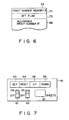
- the RAM 33 has areas that constitute a print number memory 71 for storing the print number data A retrieved from the memory card 51 as process data A', a flag memory 72 for a data set flag F which is set to "1" when a data set mode is selected, and an allowable print number memory 88 for storing the allowable print number data B retrieved from memory card 51 as process data B'.
- the operation section 41 is provided with a power switch 81, a data set mode select switch 82, a set key 83, a reset key 84, an UP key 85, a DOWN key 86 and a liquid crystal display 87.
- This display 87 displays message or numeral data such as the print number data A stored in the memory card 51.
- the CPU 31 is programmed to perform the operation shown in Fig. 8 when the power switch 81 is operated to activate the laser printer.
- the CPU 3 first executes the initialization to clear the data in the RAM 33 and reset the I/O port 34, for example. Then, the CPU 31 checks the status of the set mode select switch 82. When the switch 82 is set ON for the set mode, the data set flag F in the flag memory 72 is set to "1.” When the switch 82 is not set ON, the data set flag F in the flag memory 72 is reset to "0". After the flag F is set or reset, the CPU 31 sequentially executes a print preparation process and a print process.
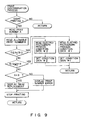
- the CPU 31 periodically executes a print discrimination process shown in Fig.9 and a key discrimination process shown in Figs. 10A and 10B.
- the CPU 31 When the print discrimination process starts, the CPU 31 first checks if a print start command is received from the host computer an set in RAM 33. This print discrimination process is immediately terminated when the print start command is not set. When it is detected that the print start command is set, the CPU 31 accesses the memory card 51 to read out the print number data A and allowable print number data B from the card 51.
- the electrophotograph process condition data #1 is read out from the condition data table 70 in the ROM 32 and various data included in this data #1 are respectively set in the D/A converters 55, 57, 59 and 60. More specifically, "-6000 V” is set as the reference voltage of the electrification voltage supply 54 in the D/A converter 55, "-5000 V” as the reference voltage of the transfer voltage supply 56 in the D/A converter 57, “-300 V” as the reference voltage of the bias voltage supply 58 in the D/A converter 59, and "3 mW" as the laser output of the laser controller 22 in the D/A converter 60.
- the electrophotograph process condition data #2 is read out from the condition data table 70 in the ROM 32 and various data included in this data #2 are respectively set in the D/A converters 55, 57, 59 and 60. More specifically, “-7000 V” is set this time as the reference voltage of the electrification voltage supply 54 in the D/A converter 55, "-6000 V” as the reference voltage of the transfer voltage supply 56 in the D/A converter 57, “-400 V” as the reference voltage of the bias voltage supply 58 in the D/A converter 59, and "4 mW" as the laser output of the laser controller 22 in the D/A converter 60.
- the CPU 31 terminates the print discrimination process after data are set in the D/A converters 55, 57, 59 and 60, so as to execute the print process.
- the electrification charger 4, laser controller 22, developing unit 6, and transfer charger 7 are activated in order to execute a sequence of electrophotograph processes based on the values set in the associated D/A converters 55, 57, 59 and 60, printing an image corresponding to print data set from the host computer on the print paper.
- the print number data A is incremented by "1" in the memory card 51.
- the CPU 31 causes the operation section interface 53 to display a message requesting replacement of the photosensitive drum 3 on the liquid crystal display 87, and inhibits the following printing operation.
- the CPU 31 causes the operation section inter face 53 to display a message, indicating that the data stored in the memory card 51 is inaccurate, on the display 87 and disables the following printing operation.
- the CPU 31 checks in step ST1 whether or not the data set keys, namely, the set key 83, reset key 84, UP key 85 and DOWN key 86, have been operated. Upon detection of the key operations in step ST1, the CPU 31 selectively performs an initializing of data A and B, an updating of data A, or an updating of data B.
- the initializing of data A and B is performed when it is confirmed that the reset key 84 has been operated, the data set flag F has been set to "1", and the set key 83 has not been operated.
- the print number data A of "0" and the allowable print number data B of "10000" are written in the memory card 51.
- the CPU 31 terminates the key discrimination process after the writing.
- the updating of data A is performed when it is confirmed that the reset key 84 has not been operated, the set key 83 has been operated, and the data set flag F has been set to "1".
- print number data A is read out from the memory card 51, and written as process data A' in the print number memory 71.
- This process data A' is read out from the memory 71 and is displayed, blinking, on the liquid crystal display 87.
- the CPU 31 repeats steps ST2 to ST4 and waits for any of the data set keys 83, 85 or 86 excluding the reset key 84 to be operated. If the operation of the UP key 85 is detected in step ST2, "100" is added to the data A' stored in the memory 71.
- the resultant data A' is read out from the memory 71 and is displayed, blinking, on the display 87.
- the CPU 31 waits for the next key operation. If the operation of the DOWN key 86 is detected in step ST3, "100" is subtracted from the data A' stored in the memory 71.
- the resultant data A' is read out from the memory 71 and is displayed, blinking, on the display 87. After the display operation, the CPU 31 waits for the next key operation. If the operation of the set key 83 is detected in step ST4, the data A' stored in the memory 71 is written as the print number data A in the memory card 51 and is displayed without blinking on the display 87. After the display operation, the CPU 31 terminates the key discrimination process.
- the updating of data B is performed when it is confirmed that the reset key 84 and set key 83 have been operated, and the data set flag F has been set to "1".
- allowable print number data B is read out from the memory card 51, and written as process data B' in the allowable print number memory 88.
- This process data B' is read out from the memory 88 and is displayed, blinking, on the liquid crystal display 87.
- the CPU 31 repeats steps ST5 to ST7 and waits for any of the data set keys 83, 85 or 86 excluding the reset key 84 to be operated. If the operation of the UP key 85 is detected in step ST5, "100" is added to the data B' stored in the memory 88.
- the resultant data B' is read out from the memory 88 and is displayed, blinking, on the display 87.
- the CPU 31 waits for the next key operation. If the operation of the DOWN key 86 is detected in step ST6, "100" is subtracted from the data B' stored in the memory 88. The resultant data B' is read out from the memory 88 and is displayed, blinking, on the display 87. After the display operation, the CPU 31 waits for the next key operation. If the operation of the set key 83 is detected in step ST7, the data B' stored in the memory 88 is written as the allowable print number data B in the memory card 51 and is displayed without blinking on the display 87. After the display operation, the CPU 31 terminates the key discrimination process.
- step ST1 If it is detected that no key operation is detected in step ST1, the operation of a key other than the set key 83 and reset key 84 is detected, or the flag F has been reset to "0", the CPU 31 will terminate the key discrimination process without doing anything.
- the data set flag F is set to "1" to select the data set mode.
- the print number data A stored in the memory card 51 connected to the card interface 52 is reset to "0.”
- the print number data A in the memory card 51 installed in the printer can be cleared to "0" by setting the power switch 81 ON after the checking with the data set mode select switch 82 rendered ON followed by the operation of the reset key 84.
- this printer can permit initialization of the memory card 51 by a simple operation without requiring a particular read/write device, and can thus improve the working efficiency in checking before shipment.
- the print number data A stored in the memory card 51 connected to the card interface 52 is read out and temporarily stored as process data A' in the print number memory 71, and the process data A' is displayed blinking on the liquid crystal display 87.
- the UP key 85 is operated in this state, "100" is added to the process data A' stored in the memory 71, and the resultant process data A' is displayed blinking on the display 87.
- the DOWN key 86 is operated, "100" is subtracted from the process data A' stored in the memory 71, and the resultant process data A' is displayed blinking on the display 87.
- the process data A' stored in the memory 71 at that point of time is written as the print number data A in the memory card 51 connected to the card interface 52. This print number data A is also displayed without blinking on the display 87.
- the data set mode select switch 82 is rendered ON, then the power switch 81 is set ON in this state followed by the operation of the set key 83.
- the print number data A stored in the memory card 51 in association with the presently mounted drum unit 2 is displayed blinking on the display 87 so that the operator writes down this number on a memo or the like.
- the UP key 85 is repeatedly operated to decrease the displayed print number by the units of "100".
- the set key 83 is operated again. Consequently, the print number close to this allowable print number is written in the memory card 51. It is therefore possible to check if a message requesting the drum replacement is displayed by actually making prints until the print number reaches the allowable print number.
- the set key 83 is operated again with the set mode selected. Then the DOWN key 86 is repeatedly operated to decrement the displayed print number by the units of "100".
- the set key 83 is operated again to write the present print number data in the memory card 51. Therefore, the printing history of the photosensitive drum in the laser printer can be set back to the correct value as before the maintenance inspection. Accordingly, it is possible to check if an alarm indication is made when the print number reaches the allowable print number in the maintenance inspection or the like by a simple key operation without requiring a read/write device. This can therefore ensure easier maintenance inspection.
- the presently installed memory card may be replaced with another memory card and the print number data recorded in the new memory card may be arbitrarily altered.
- the allowable print number data B stored in the memory card 51 connected to the card interface 52 is read out and temporarily stored as process data B' in the allowable print number memory 88, and the process data B' is displayed blinking on the liquid crystal display 87.
- the process data B' stored in the memory 88 increases or decreases by the units of "100”, and the resultant process data B' is displayed blinking on the display 87.
- the process data B' stored in the memory 88 at that point of time is written as the allowable print number data B in the memory card 51 connected to the card interface 52.
- This allowable print number data B is also displayed without blinking on the display 87. Since the allowable print number B can be updated, it is possible to cope with the case where the service life of the photosensitive drum is changed by replacement of the drum unit.
- the present invention is not limited to the above-described embodiment, and can be modified in other various manners without departing from the scope and spirit thereof.
- the UP key 85 and DOWN key 86 are provided to increase and decrease the number data stored in the memory card 51 by the units of "100". Instead, numerical keys may be provided to directly set the desired number, for example.
- the memory card 51 is used as an example of the data recording medium in the above embodiment, a magnetic tape or other types of recording media may be employed as well.
- the recording medium may also be a semiconductor memory such as E2 PROM or RAM with power backup.
- the present invention is not restricted to a laser printer, but may also be applied to a copying machine in which a drum unit having a photosensitive member is detachably mounted to the cabinet.
Landscapes
- Physics & Mathematics (AREA)
- General Physics & Mathematics (AREA)
- Engineering & Computer Science (AREA)
- Computer Vision & Pattern Recognition (AREA)
- Control Or Security For Electrophotography (AREA)
- Accessory Devices And Overall Control Thereof (AREA)
- Laser Beam Printer (AREA)
- Counters In Electrophotography And Two-Sided Copying (AREA)
Applications Claiming Priority (2)
| Application Number | Priority Date | Filing Date | Title |
|---|---|---|---|
| JP2009557A JPH03214170A (ja) | 1990-01-19 | 1990-01-19 | 電子写真装置 |
| JP9557/90 | 1990-01-19 |
Publications (3)
| Publication Number | Publication Date |
|---|---|
| EP0438160A2 true EP0438160A2 (fr) | 1991-07-24 |
| EP0438160A3 EP0438160A3 (en) | 1992-05-13 |
| EP0438160B1 EP0438160B1 (fr) | 1994-09-14 |
Family
ID=11723586
Family Applications (1)
| Application Number | Title | Priority Date | Filing Date |
|---|---|---|---|
| EP91100555A Expired - Lifetime EP0438160B1 (fr) | 1990-01-19 | 1991-01-18 | Appareil électrophotographique |
Country Status (4)
| Country | Link |
|---|---|
| EP (1) | EP0438160B1 (fr) |
| JP (1) | JPH03214170A (fr) |
| KR (1) | KR940002424B1 (fr) |
| DE (1) | DE69103914T2 (fr) |
Cited By (2)
| Publication number | Priority date | Publication date | Assignee | Title |
|---|---|---|---|---|
| EP0579358A1 (fr) * | 1992-07-10 | 1994-01-19 | Brother Kogyo Kabushiki Kaisha | Appareil de formation d'images à function d'impression automatique |
| EP0784249A3 (fr) * | 1996-01-09 | 1998-11-11 | Canon Kabushiki Kaisha | Appareil de formation d'images en unité montée dans cet appareil |
Families Citing this family (1)
| Publication number | Priority date | Publication date | Assignee | Title |
|---|---|---|---|---|
| KR101981578B1 (ko) | 2016-12-12 | 2019-05-23 | 정철 | 이형몰드를 이용하는 패턴형성방법 |
Family Cites Families (2)
| Publication number | Priority date | Publication date | Assignee | Title |
|---|---|---|---|---|
| JPH02559A (ja) * | 1987-10-30 | 1990-01-05 | Ricoh Co Ltd | 画像形成装置 |
| JPH01263662A (ja) * | 1988-04-15 | 1989-10-20 | Fuji Xerox Co Ltd | 記録装置およびその消耗部品 |
-
1990
- 1990-01-19 JP JP2009557A patent/JPH03214170A/ja active Pending
-
1991
- 1991-01-18 EP EP91100555A patent/EP0438160B1/fr not_active Expired - Lifetime
- 1991-01-18 DE DE69103914T patent/DE69103914T2/de not_active Expired - Fee Related
- 1991-01-18 KR KR1019910000828A patent/KR940002424B1/ko not_active Expired - Fee Related
Cited By (4)
| Publication number | Priority date | Publication date | Assignee | Title |
|---|---|---|---|---|
| EP0579358A1 (fr) * | 1992-07-10 | 1994-01-19 | Brother Kogyo Kabushiki Kaisha | Appareil de formation d'images à function d'impression automatique |
| US5506943A (en) * | 1992-07-10 | 1996-04-09 | Brother Kogyo Kabushiki Kaisha | Image forming apparatus having automatic printing function |
| EP0784249A3 (fr) * | 1996-01-09 | 1998-11-11 | Canon Kabushiki Kaisha | Appareil de formation d'images en unité montée dans cet appareil |
| US6163658A (en) * | 1996-01-09 | 2000-12-19 | Canon Kabushiki Kaisha | Process cartridge for storing compressed information detachably mountable to a main assembly of an image forming apparatus, and an image forming apparatus including such cartridge |
Also Published As
| Publication number | Publication date |
|---|---|
| KR910014771A (ko) | 1991-08-31 |
| EP0438160A3 (en) | 1992-05-13 |
| KR940002424B1 (ko) | 1994-03-24 |
| EP0438160B1 (fr) | 1994-09-14 |
| DE69103914D1 (de) | 1994-10-20 |
| JPH03214170A (ja) | 1991-09-19 |
| DE69103914T2 (de) | 1995-01-05 |
Similar Documents
| Publication | Publication Date | Title |
|---|---|---|
| EP1217456B1 (fr) | Système de sécurité pour composants interchangeables | |
| JP2602341B2 (ja) | 静電写真式複製装置の監視保証方法 | |
| USRE35751E (en) | Monitoring system with dual memory for electrophotographic printing machines using replaceable cartridges | |
| JPH0243636B2 (fr) | ||
| US20020171703A1 (en) | Printer cartridge with memory for printer control and adjustment of printer settings | |
| US5276461A (en) | Electrophotographic printing device | |
| KR0177099B1 (ko) | 화상 형성장치의 상태메세지 출력방법 | |
| JPH1067158A (ja) | 画像形成装置 | |
| JP2002169431A (ja) | 画像形成装置、画像形成装置に用いる交換部品及びicチップ | |
| US20030123887A1 (en) | Adertising from the customer replaceable unit memory of a copier or printer cartridge | |
| EP0438160B1 (fr) | Appareil électrophotographique | |
| JPH07175373A (ja) | 電子装置 | |
| JPH02559A (ja) | 画像形成装置 | |
| EP1184734B1 (fr) | Dispositif de formation d'image | |
| JPH04299375A (ja) | 電子写真装置 | |
| JPH03230172A (ja) | 画像形成装置 | |
| JP2690414B2 (ja) | 電子写真装置 | |
| JPH06324536A (ja) | カラー画像形成装置 | |
| JP3342115B2 (ja) | 印刷装置 | |
| KR101123702B1 (ko) | 화상형성장치 및 그의 인쇄방법 | |
| JPH0667483A (ja) | ドラム周辺ユニットの通信エラー防止装置 | |
| JPH04326365A (ja) | 電子写真装置 | |
| JPH04107483A (ja) | 電子写真装置 | |
| JPH0973254A (ja) | 画像形成装置の制御方式 | |
| JPH03209271A (ja) | 電子写真装置 |
Legal Events
| Date | Code | Title | Description |
|---|---|---|---|
| PUAI | Public reference made under article 153(3) epc to a published international application that has entered the european phase |
Free format text: ORIGINAL CODE: 0009012 |
|
| 17P | Request for examination filed |
Effective date: 19910118 |
|
| AK | Designated contracting states |
Kind code of ref document: A2 Designated state(s): DE FR GB IT |
|
| PUAL | Search report despatched |
Free format text: ORIGINAL CODE: 0009013 |
|
| AK | Designated contracting states |
Kind code of ref document: A3 Designated state(s): DE FR GB IT |
|
| 17Q | First examination report despatched |
Effective date: 19930819 |
|
| GRAA | (expected) grant |
Free format text: ORIGINAL CODE: 0009210 |
|
| AK | Designated contracting states |
Kind code of ref document: B1 Designated state(s): DE FR GB IT |
|
| ITF | It: translation for a ep patent filed | ||
| REF | Corresponds to: |
Ref document number: 69103914 Country of ref document: DE Date of ref document: 19941020 |
|
| ET | Fr: translation filed | ||
| PLBE | No opposition filed within time limit |
Free format text: ORIGINAL CODE: 0009261 |
|
| STAA | Information on the status of an ep patent application or granted ep patent |
Free format text: STATUS: NO OPPOSITION FILED WITHIN TIME LIMIT |
|
| 26N | No opposition filed | ||
| REG | Reference to a national code |
Ref country code: GB Ref legal event code: IF02 |
|
| PGFP | Annual fee paid to national office [announced via postgrant information from national office to epo] |
Ref country code: FR Payment date: 20030110 Year of fee payment: 13 |
|
| PGFP | Annual fee paid to national office [announced via postgrant information from national office to epo] |
Ref country code: GB Payment date: 20030115 Year of fee payment: 13 |
|
| PGFP | Annual fee paid to national office [announced via postgrant information from national office to epo] |
Ref country code: DE Payment date: 20030130 Year of fee payment: 13 |
|
| PG25 | Lapsed in a contracting state [announced via postgrant information from national office to epo] |
Ref country code: GB Free format text: LAPSE BECAUSE OF NON-PAYMENT OF DUE FEES Effective date: 20040118 |
|
| PG25 | Lapsed in a contracting state [announced via postgrant information from national office to epo] |
Ref country code: DE Free format text: LAPSE BECAUSE OF NON-PAYMENT OF DUE FEES Effective date: 20040803 |
|
| GBPC | Gb: european patent ceased through non-payment of renewal fee |
Effective date: 20040118 |
|
| PG25 | Lapsed in a contracting state [announced via postgrant information from national office to epo] |
Ref country code: FR Free format text: LAPSE BECAUSE OF NON-PAYMENT OF DUE FEES Effective date: 20040930 |
|
| REG | Reference to a national code |
Ref country code: FR Ref legal event code: ST |
|
| PG25 | Lapsed in a contracting state [announced via postgrant information from national office to epo] |
Ref country code: IT Free format text: LAPSE BECAUSE OF NON-PAYMENT OF DUE FEES;WARNING: LAPSES OF ITALIAN PATENTS WITH EFFECTIVE DATE BEFORE 2007 MAY HAVE OCCURRED AT ANY TIME BEFORE 2007. THE CORRECT EFFECTIVE DATE MAY BE DIFFERENT FROM THE ONE RECORDED. Effective date: 20050118 |