EP0438959A2 - Dispositif semi-conducteur utilisant une structure épitaxiale à multi-couches et son procédé de fabrication - Google Patents
Dispositif semi-conducteur utilisant une structure épitaxiale à multi-couches et son procédé de fabrication Download PDFInfo
- Publication number
- EP0438959A2 EP0438959A2 EP90480214A EP90480214A EP0438959A2 EP 0438959 A2 EP0438959 A2 EP 0438959A2 EP 90480214 A EP90480214 A EP 90480214A EP 90480214 A EP90480214 A EP 90480214A EP 0438959 A2 EP0438959 A2 EP 0438959A2
- Authority
- EP
- European Patent Office
- Prior art keywords
- layer
- dopant concentration
- substrate
- range
- atoms
- Prior art date
- Legal status (The legal status is an assumption and is not a legal conclusion. Google has not performed a legal analysis and makes no representation as to the accuracy of the status listed.)
- Withdrawn
Links
Images

Classifications
-
- H—ELECTRICITY
- H10—SEMICONDUCTOR DEVICES; ELECTRIC SOLID-STATE DEVICES NOT OTHERWISE PROVIDED FOR
- H10W—GENERIC PACKAGES, INTERCONNECTIONS, CONNECTORS OR OTHER CONSTRUCTIONAL DETAILS OF DEVICES COVERED BY CLASS H10
- H10W10/00—Isolation regions in semiconductor bodies between components of integrated devices
- H10W10/01—Manufacture or treatment
- H10W10/011—Manufacture or treatment of isolation regions comprising dielectric materials
- H10W10/012—Manufacture or treatment of isolation regions comprising dielectric materials using local oxidation of silicon [LOCOS]
-
- H—ELECTRICITY
- H10—SEMICONDUCTOR DEVICES; ELECTRIC SOLID-STATE DEVICES NOT OTHERWISE PROVIDED FOR
- H10P—GENERIC PROCESSES OR APPARATUS FOR THE MANUFACTURE OR TREATMENT OF DEVICES COVERED BY CLASS H10
- H10P14/00—Formation of materials, e.g. in the shape of layers or pillars
- H10P14/20—Formation of materials, e.g. in the shape of layers or pillars of semiconductor materials
- H10P14/24—Formation of materials, e.g. in the shape of layers or pillars of semiconductor materials using chemical vapour deposition [CVD]
-
- H—ELECTRICITY
- H10—SEMICONDUCTOR DEVICES; ELECTRIC SOLID-STATE DEVICES NOT OTHERWISE PROVIDED FOR
- H10P—GENERIC PROCESSES OR APPARATUS FOR THE MANUFACTURE OR TREATMENT OF DEVICES COVERED BY CLASS H10
- H10P14/00—Formation of materials, e.g. in the shape of layers or pillars
- H10P14/20—Formation of materials, e.g. in the shape of layers or pillars of semiconductor materials
- H10P14/29—Formation of materials, e.g. in the shape of layers or pillars of semiconductor materials characterised by the substrates
- H10P14/2901—Materials
- H10P14/2902—Materials being Group IVA materials
- H10P14/2905—Silicon, silicon germanium or germanium
-
- H—ELECTRICITY
- H10—SEMICONDUCTOR DEVICES; ELECTRIC SOLID-STATE DEVICES NOT OTHERWISE PROVIDED FOR
- H10P—GENERIC PROCESSES OR APPARATUS FOR THE MANUFACTURE OR TREATMENT OF DEVICES COVERED BY CLASS H10
- H10P14/00—Formation of materials, e.g. in the shape of layers or pillars
- H10P14/20—Formation of materials, e.g. in the shape of layers or pillars of semiconductor materials
- H10P14/29—Formation of materials, e.g. in the shape of layers or pillars of semiconductor materials characterised by the substrates
- H10P14/2926—Crystal orientations
-
- H—ELECTRICITY
- H10—SEMICONDUCTOR DEVICES; ELECTRIC SOLID-STATE DEVICES NOT OTHERWISE PROVIDED FOR
- H10P—GENERIC PROCESSES OR APPARATUS FOR THE MANUFACTURE OR TREATMENT OF DEVICES COVERED BY CLASS H10
- H10P14/00—Formation of materials, e.g. in the shape of layers or pillars
- H10P14/20—Formation of materials, e.g. in the shape of layers or pillars of semiconductor materials
- H10P14/34—Deposited materials, e.g. layers
- H10P14/3402—Deposited materials, e.g. layers characterised by the chemical composition
- H10P14/3404—Deposited materials, e.g. layers characterised by the chemical composition being Group IVA materials
- H10P14/3411—Silicon, silicon germanium or germanium
-
- H—ELECTRICITY
- H10—SEMICONDUCTOR DEVICES; ELECTRIC SOLID-STATE DEVICES NOT OTHERWISE PROVIDED FOR
- H10W—GENERIC PACKAGES, INTERCONNECTIONS, CONNECTORS OR OTHER CONSTRUCTIONAL DETAILS OF DEVICES COVERED BY CLASS H10
- H10W10/00—Isolation regions in semiconductor bodies between components of integrated devices
- H10W10/01—Manufacture or treatment
- H10W10/011—Manufacture or treatment of isolation regions comprising dielectric materials
-
- H—ELECTRICITY
- H10—SEMICONDUCTOR DEVICES; ELECTRIC SOLID-STATE DEVICES NOT OTHERWISE PROVIDED FOR
- H10W—GENERIC PACKAGES, INTERCONNECTIONS, CONNECTORS OR OTHER CONSTRUCTIONAL DETAILS OF DEVICES COVERED BY CLASS H10
- H10W10/00—Isolation regions in semiconductor bodies between components of integrated devices
- H10W10/01—Manufacture or treatment
- H10W10/011—Manufacture or treatment of isolation regions comprising dielectric materials
- H10W10/014—Manufacture or treatment of isolation regions comprising dielectric materials using trench refilling with dielectric materials, e.g. shallow trench isolations
-
- H—ELECTRICITY
- H10—SEMICONDUCTOR DEVICES; ELECTRIC SOLID-STATE DEVICES NOT OTHERWISE PROVIDED FOR
- H10W—GENERIC PACKAGES, INTERCONNECTIONS, CONNECTORS OR OTHER CONSTRUCTIONAL DETAILS OF DEVICES COVERED BY CLASS H10
- H10W10/00—Isolation regions in semiconductor bodies between components of integrated devices
- H10W10/10—Isolation regions comprising dielectric materials
-
- H—ELECTRICITY
- H10—SEMICONDUCTOR DEVICES; ELECTRIC SOLID-STATE DEVICES NOT OTHERWISE PROVIDED FOR
- H10W—GENERIC PACKAGES, INTERCONNECTIONS, CONNECTORS OR OTHER CONSTRUCTIONAL DETAILS OF DEVICES COVERED BY CLASS H10
- H10W10/00—Isolation regions in semiconductor bodies between components of integrated devices
- H10W10/10—Isolation regions comprising dielectric materials
- H10W10/13—Isolation regions comprising dielectric materials formed using local oxidation of silicon [LOCOS], e.g. sealed interface localised oxidation [SILO] or side-wall mask isolation [SWAMI]
-
- H—ELECTRICITY
- H10—SEMICONDUCTOR DEVICES; ELECTRIC SOLID-STATE DEVICES NOT OTHERWISE PROVIDED FOR
- H10W—GENERIC PACKAGES, INTERCONNECTIONS, CONNECTORS OR OTHER CONSTRUCTIONAL DETAILS OF DEVICES COVERED BY CLASS H10
- H10W10/00—Isolation regions in semiconductor bodies between components of integrated devices
- H10W10/10—Isolation regions comprising dielectric materials
- H10W10/17—Isolation regions comprising dielectric materials formed using trench refilling with dielectric materials, e.g. shallow trench isolations
-
- H—ELECTRICITY
- H10—SEMICONDUCTOR DEVICES; ELECTRIC SOLID-STATE DEVICES NOT OTHERWISE PROVIDED FOR
- H10W—GENERIC PACKAGES, INTERCONNECTIONS, CONNECTORS OR OTHER CONSTRUCTIONAL DETAILS OF DEVICES COVERED BY CLASS H10
- H10W15/00—Highly-doped buried regions of integrated devices
-
- H—ELECTRICITY
- H10—SEMICONDUCTOR DEVICES; ELECTRIC SOLID-STATE DEVICES NOT OTHERWISE PROVIDED FOR
- H10W—GENERIC PACKAGES, INTERCONNECTIONS, CONNECTORS OR OTHER CONSTRUCTIONAL DETAILS OF DEVICES COVERED BY CLASS H10
- H10W15/00—Highly-doped buried regions of integrated devices
- H10W15/01—Manufacture or treatment
Definitions
- the present invention relates generally to semiconductor devices and more particularly to a semiconductor device structure incorporating a multi-level structure including a highly doped buffer layer, and a method of manufacturing the same.
- typical semiconductor device structures utilize a relatively highly doped P+ 10 (FIG. 1) or N+ 12 (FIG. 2) substrate having, for example, a dopant concentration generally higher than 1017 atoms/cubic centimeter.
- Substrates 10 and 12 are formed using a conventional crystal pulling process so as to have a surface orientation of, for example, ⁇ 100>, ⁇ 110>, or ⁇ 111>.
- a relatively lightly doped P ⁇ epitaxial layer 13 is formed on substrate 10, and isolation regions 14 of an insulating material are formed from the surface of layer 13 downward into layer 10 to form an isolated device region 15.
- FIG. 2 shows the same type of isolated device region 22 formed in a lightly doped N ⁇ epitaxial layer 20.
- a protective capping layer 16 of silicon dioxide is formed on the backside of the substrate to prevent autodoping of the epitaxial layer by the substrate.
- passive devices such as resistors (not shown), and/or active devices (not shown) such as bipolar transistors, field-effect transistors, BICMOS circuits, or integrated circuits are formed in the isolated device regions 15, 22.
- active devices typically includes the formation of multiple doped regions (not shown) within the epitaxial la yers 13, 20 of device regions 15 and 22.
- U.S. patent no. 3 585 464 to Castrucci et al. shows a different semiconductor device structure wherein an epitaxial N layer is formed on a P ⁇ substrate. Active devices are subsequently formed in isolated regions of the N layer. The forming of the device-containing layer directly on the lightly doped substrate results in the disadvantage of less than optimal electrical isolation between isolated device regions.
- Hays patent no. 3 721 588 to Hays shows a method wherein a lightly doped substrate 10 is used to support a first highly doped epitaxial layer 11.
- the Hays patent teaches the removal of the substrate and the first epitaxial layer to leave a thin, second epitaxial silicon layer supported on an insulator.
- a further object of the present invention is to provide such a structure and process wherein the doping concentration profile of the device regions can be very closely controlled.
- An additional object of the present invention is to provide such a structure and process wherein the oxygen and other impurities in the device regions can be minimized so as to reduce electrical defects.
- An additional object of the present invention is to provide such a structure and process wherein the oxygen and other impurities in the device regions can be minimized so as to reduce electrical defects.
- Yet another object of the present invention is to provide such a structure and process which is compatible with existing semiconductor processes.
- Yet a further object of the present invention is to provide such a structure and process which requires less processing steps and hence which is more economical than the prior art.
- a new and improved semiconductor structure comprising: a doped semiconductor substrate including a surface; a first layer of epitaxial semiconductor material on the substrate surface having a relatively higher dopant concentration than the substrate; a second layer of epitaxial semiconductor material on the first layer, the second layer having a relatively lower dopant concentration than the first layer; and isolation means including a region of insulating material extending from a surface of t he second layer into the first layer for electrically isolating a device region in the second layer.
- a new and improved method of forming a semiconductor structure comprising the steps of: providing a doped semiconductor substrate including a surface; epitaxially growing a first layer of semiconductor material on the sub strate surface, the first layer having a relatively higher dopant concentration than the substrate; epitaxially growing a second layer of semiconductor material on the first layer, the second layer having a relatively lower dopant concentration than the first layer; forming isolation means including a region of insulating material extending from a surface of the second layer into the first layer for electrically isolating a device region in the second layer.
- a silicon semiconductor structure 30 formed in accordance with the present invention includes a substrate 32 defining a generally planar surface overlain by a multilevel, silicon epitaxial structure 34.
- Substrate 32 comprises a conventional silicon crystal formed by a conventional, liquid growth crystal pulling process to form, for example a ⁇ 100>, ⁇ 110>, or ⁇ 111> crystallographic orientation.
- Substrate 32 is doped in a conventional manner during the manufacturing process with either a P or N type dopant to a concentration in the range of from 1014-1019 dopant atoms per cubic centimeter (atoms/ cc).
- a typical, preferred concentration for substrate 32 is less than 1017 atoms/cc.
- substrate 32 will contain an inherent oxygen concentration in the range of about 3-40 interstitial oxygen atoms per million silicon atoms (ppma) (ASTM F121-79). It will be appreciated that, when the doping concentration of substrate 32 is kept relatively light, i.e. in the preferred range below about 1017 atoms/cc, the oxygen concentration in the substrate can be easily measured and controlled.
- epitaxial structure 34 comprises a highly doped P+ or N+ epitaxial buffer layer 36 formed on substrate 32.
- Layer 36 is formed to a thickness in the range of about 0.4-20 micrometers, and to a doping concentration in the range of 1017-1020 atoms/cc. Typical thicknesses and dopant concentrations for layer 36 are about 12 micrometers and 1019 atoms/cc, respectively.
- Epitaxial structure 34 including layer 36 and subsequently formed layer 38 and 40 (described below), is formed using conventional processes and tools in the manner described below.
- Epitaxial layers 36, 38, and 40 are grown at a temperature in the range of 850-1200 degrees centigrade and at a growth rate of about 0.1-6.0 microns/minute.
- a typical temperature and growth rate comprises, for example, 1130 degrees centigrade and 2 microns/minute, respectively.
- the growth rate is dependent upon such factors as the silicon source species (e.g. SiH x Cl y or SiH4), the reactor main flow rate and geometry, and the selected deposition temperature.
- the dopant concentration within the reactor is selected to provide the desired, resultant substrate concentration, and is dependent on the layer growth rate and the dopant specie incorporation rate into the grown layer.
- buffer layer 36 can beneficially be doped with Group IV impurity atoms such as germanium (Ge).
- Group IV impurity atoms such as germanium (Ge).
- Ge germanium
- Such impurity doping when performed to a ration of about 1:10, dopant:species, provides the significant advantage of reducing wafer distortion by matching lattice constants. This results in substantially decreased wafer warpage and a concomitant decrease in electrical defects.
- Epitaxial silicon layer 38 is formed over layer 36 to a thickness in the range of 0.0-2.0 microns and an intrinsic dopant concentration of less than 1015 atoms/cc.
- a typical thickness for layer 38 is on the order of about 0.4 micrometers, while the dopant concentration is preferably intrinsic - i.e. maintained as low as possible by avoiding deliberate doping.
- layer 38 comprises an optional feature of the present invention.
- the device is subjected to a cleaning process of the above-described type, and a layer 40 of N or P type doped epitaxial silicon is formed over layer 38.
- Layer 40 is formed to a thickness in the range of 0.4-10 micrometers, and a concentration in the range of 1015-1017 atoms/cc.
- a typical thickness and dopant concentration for layer 40 comprises 2.0 microns and 1016 atoms/cc, respectively.
- layer 40 comprises the device-supporting layer.
- Isolating regions 42A, 42B are formed in structure 30, extending from the upper surface of layer 40 and terminating in layer 36. It is an important feature of the present invention that isolating regions 42A and 42B terminate in highly doped layer 36, and do not extend into substrate 32 as is commonly practiced in the prior art. In a manner well known in the art, isolating regions 42A, 42B can, for example, comprise portions of a circular or rectangular isolation structure so as to circumscribe an isolated device region 40A in layer 40.
- isolation regions 42A, 42B these isolation regions can comprise, for example, multi-layer insulating materials in the manner shown and described in U.S. patents 4 104 086 or 4 307 180, each of which is assigne d to the assignee of the present invention and incorporated herein by reference.
- isolation regions 42A, 42B can be formed such that selected ones of the regions provide an electrical connection to layer 36.
- selected isolation regions include insulating sidewalls, open bottoms (i.e. the insulating sidewalls do not extend to the region/trench bottoms), and a conductive filler such as polysilicon.
- a conductive filler such as polysilicon.
- electrical connection to layer 36 can be made by the use of a heavily doped silicon region, formed by high temperature diffusion processing, in a manner well known in the art.
- Isolation trenches 42A, 42B thus define isolated device region 40A within layer 40 wherein active devices and/or inactive devices are subsequently formed.
- the doping concentrations of vapor grown, epitaxial layers 36, 38 and 40 can be very closely controlled. These same epitaxial layers contain virtually no oxygen precipitates.
- the interstitial oxygen in the substrate is more readily measured and controlled than with more highly doped substrates. This results in fewer electrical defects in the substrate.
- the electrical isolation of isolated device region 40A is very good because of the isolating effect of highly doped layer 36.
- the step of forming the silicon dioxide capping layer (16 of FIGS. 1 and 2), and the warpage and extra process steps associated therewith, is avoided.
- Yet a further advantage of the present invention is the tendency of heavily doped layer 36 to absorb alpha particles, minimizing the sensitivity of devices formed in structure 30 to alpha particle radiation.
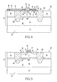
- the semiconductor structure 30 of FIG. 3 is shown supporting a vertical NPN transistor 44 in isolated device region 40A.
- substrate 32 and epitaxial layers 36, 38, and 40 are formed so as to have dopant concen trations of: 1016 P type, 1019 P type, undoped, and 1016 N type, respectively.
- Transistor 44 includes a P type base region 46 extending from the surface of region 40A into the region, and an N type emitter region 48 extending from the same surface into the base region.
- a shallow insulating region 50 is positioned in the surface of region 40A intermediate base region 46 and isolation region 42B.
- Electrical contacts to transistor 44 include a polysilicon base contact 52 to the extrinsic edges of base region 46, a metal or polysilicon emitter contact 54 to emitter region 48, and a metal or polysilicon collector contact 56 to a portion of region 40A adjoining isolation region 50.
- a thin layer of insulating material 58 for example a stack of silicon nitride over silicon oxide, separates contact 52 from structure 30 excepting where physical contact is made to base region 46.
- Insulating sidewalls 60 for example comprising silicon dioxide, silicon nitride, or a stack of these two materials, cover and insulate the vertical walls of contacts 52.
- An insulating overlay 61 again comprising, for example, silicon dioxide, silicon nitride, or a multilayer stack of the same, overlies the upper surface of extrinsic base contact 52.
- transis tor 44 Many methods of forming the structure of transis tor 44 are known to those skilled in the art, includ ing such methods as those shown in U.S. patents 4 319 932, 4 160 991, 4 157 269, 4 252 582. Each of these patents is assigned to the assignee of the present invention and incorporated herein by reference.
- FIG. 5 another embodiment of The present invention is shown wherein an insulated gate, or field-effect transistor (FET) 64 is shown formed in isolated device region 40A.
- FET field-effect transistor
- substrate 32 and epitaxial layers 36, 38, and 40 are formed so as to have dopant concentrations of: 1016 P type, 1018 N type, undoped, and 1016 P type, respectively.
- FET 64 includes highly doped, N+ source and drain regions 66, 68, respectively, in the surface of isolated device region 40A. These source and drain regions 66 and 68 are spaced by a channel region 70 in layer 40. Channel region 70 is positioned underneath a gate structure comprising a conductive gate elec trode 74 spaced from the channel by a thin layer of insulating material 72. Electrode 74 can comprise, for example, metal or doped polysilicon, while insu lating layer 72 can comprise, for example, silicon dioxide. Many methods are known in the art for forming FET 64 and similar field-effect transistor structures, and need not be detailed herein.
- bipolar tran sistor 44 (FIG. 4) or FET 64 (FIG. 5) does not comprise a main aspect of the present invention.
- the benefits of the present invention are achieved through the use of semiconductor structure 30, with active and/or passive (not shown) devices formed in isolated device region 40A. Because structure 30 exhibits the above-described advantages of well-controlled doping profiles, low defects and impurities, and good elec trical isolation of the isolated device regions, devices formed within these isolated device regions exhibit the benefit from concomitant advantages.
- the doping concentrations and profiles of devices formed in isolated device region 40A of structure 30 are capable of highly accurate control.
- the lack of defects and impurities in structure 30 provides for high performance, high yield, high reliability devices.
- the good electrical isolation of the isolated device regions results in devices having improved operating characteristics.
- intrinsic layer 38 while desirable in that it minimizes autodoping from highly doped buffer layer 36 into device layer 40, is not necessary to the practice of the present invention.
- the advantages of the invention can be achieved through the use of substrate 32 in combination with the multilevel epitaxial layers including highly doped layer 36 and layer 40 in which the devices are formed.
- a new and improved semi conductor device structure including a substrate overlain by a multilevel epitaxial structure including a first, highly doped epitaxial layer, and a second, device-supporting layer.
- the invention has application in the formation of semiconductor devices, and particularly in the field of very large scale integrated (VLS I)- and ultra large scale integrated (ULSI) circuit semiconductor device manufacturing.
- VLS I very large scale integrated
- ULSI ultra large scale integrated
Landscapes
- Element Separation (AREA)
- Bipolar Transistors (AREA)
- Insulated Gate Type Field-Effect Transistor (AREA)
- Recrystallisation Techniques (AREA)
Applications Claiming Priority (2)
| Application Number | Priority Date | Filing Date | Title |
|---|---|---|---|
| US07/468,533 US5061652A (en) | 1990-01-23 | 1990-01-23 | Method of manufacturing a semiconductor device structure employing a multi-level epitaxial structure |
| US468533 | 1990-01-23 |
Publications (2)
| Publication Number | Publication Date |
|---|---|
| EP0438959A2 true EP0438959A2 (fr) | 1991-07-31 |
| EP0438959A3 EP0438959A3 (en) | 1993-03-10 |
Family
ID=23860198
Family Applications (1)
| Application Number | Title | Priority Date | Filing Date |
|---|---|---|---|
| EP19900480214 Withdrawn EP0438959A3 (en) | 1990-01-23 | 1990-12-12 | Semiconductor device structure employing a multi-level epitaxial structure and a method of manufacturing same |
Country Status (3)
| Country | Link |
|---|---|
| US (1) | US5061652A (fr) |
| EP (1) | EP0438959A3 (fr) |
| JP (1) | JPH0697666B2 (fr) |
Cited By (2)
| Publication number | Priority date | Publication date | Assignee | Title |
|---|---|---|---|---|
| EP0518325A3 (en) * | 1991-06-13 | 1993-03-17 | Wacker-Chemitronic Gesellschaft Fuer Elektronik-Grundstoffe Mbh | Epitaxial semiconductor chip with low oxygen zone of adjustable thickness and process of making same |
| SG100757A1 (en) * | 2000-10-20 | 2003-12-26 | Ibm | Fully-depleted-collector silicon-on-insulator (soi) bipolar transistor useful alone or in soi bicmos |
Families Citing this family (37)
| Publication number | Priority date | Publication date | Assignee | Title |
|---|---|---|---|---|
| KR940006696B1 (ko) * | 1991-01-16 | 1994-07-25 | 금성일렉트론 주식회사 | 반도체 소자의 격리막 형성방법 |
| JPH06260552A (ja) * | 1993-03-09 | 1994-09-16 | Mitsubishi Electric Corp | 化合物半導体装置の素子分離方法、及び化合物半導体装置 |
| US6133615A (en) * | 1998-04-13 | 2000-10-17 | Wisconsin Alumni Research Foundation | Photodiode arrays having minimized cross-talk between diodes |
| US6452220B1 (en) | 1999-12-09 | 2002-09-17 | The Regents Of The University Of California | Current isolating epitaxial buffer layers for high voltage photodiode array |
| US6492237B2 (en) * | 2001-02-12 | 2002-12-10 | Maxim Integrated Products, Inc. | Method of forming an NPN device |
| US6720595B2 (en) * | 2001-08-06 | 2004-04-13 | International Business Machines Corporation | Three-dimensional island pixel photo-sensor |
| US6767798B2 (en) * | 2002-04-09 | 2004-07-27 | Maxim Integrated Products, Inc. | Method of forming self-aligned NPN transistor with raised extrinsic base |
| US7402870B2 (en) * | 2004-10-12 | 2008-07-22 | International Business Machines Corporation | Ultra shallow junction formation by epitaxial interface limited diffusion |
| US9520486B2 (en) | 2009-11-04 | 2016-12-13 | Analog Devices, Inc. | Electrostatic protection device |
| US8665571B2 (en) | 2011-05-18 | 2014-03-04 | Analog Devices, Inc. | Apparatus and method for integrated circuit protection |
| US8432651B2 (en) | 2010-06-09 | 2013-04-30 | Analog Devices, Inc. | Apparatus and method for electronic systems reliability |
| US10199482B2 (en) | 2010-11-29 | 2019-02-05 | Analog Devices, Inc. | Apparatus for electrostatic discharge protection |
| US8466489B2 (en) | 2011-02-04 | 2013-06-18 | Analog Devices, Inc. | Apparatus and method for transient electrical overstress protection |
| US8592860B2 (en) | 2011-02-11 | 2013-11-26 | Analog Devices, Inc. | Apparatus and method for protection of electronic circuits operating under high stress conditions |
| US8680620B2 (en) | 2011-08-04 | 2014-03-25 | Analog Devices, Inc. | Bi-directional blocking voltage protection devices and methods of forming the same |
| US8947841B2 (en) | 2012-02-13 | 2015-02-03 | Analog Devices, Inc. | Protection systems for integrated circuits and methods of forming the same |
| US8829570B2 (en) | 2012-03-09 | 2014-09-09 | Analog Devices, Inc. | Switching device for heterojunction integrated circuits and methods of forming the same |
| US8946822B2 (en) | 2012-03-19 | 2015-02-03 | Analog Devices, Inc. | Apparatus and method for protection of precision mixed-signal electronic circuits |
| US8610251B1 (en) * | 2012-06-01 | 2013-12-17 | Analog Devices, Inc. | Low voltage protection devices for precision transceivers and methods of forming the same |
| US8637899B2 (en) | 2012-06-08 | 2014-01-28 | Analog Devices, Inc. | Method and apparatus for protection and high voltage isolation of low voltage communication interface terminals |
| US8796729B2 (en) | 2012-11-20 | 2014-08-05 | Analog Devices, Inc. | Junction-isolated blocking voltage devices with integrated protection structures and methods of forming the same |
| US9123540B2 (en) | 2013-01-30 | 2015-09-01 | Analog Devices, Inc. | Apparatus for high speed signal processing interface |
| US8860080B2 (en) | 2012-12-19 | 2014-10-14 | Analog Devices, Inc. | Interface protection device with integrated supply clamp and method of forming the same |
| US9006781B2 (en) | 2012-12-19 | 2015-04-14 | Analog Devices, Inc. | Devices for monolithic data conversion interface protection and methods of forming the same |
| US9275991B2 (en) | 2013-02-13 | 2016-03-01 | Analog Devices, Inc. | Apparatus for transceiver signal isolation and voltage clamp |
| US9147677B2 (en) | 2013-05-16 | 2015-09-29 | Analog Devices Global | Dual-tub junction-isolated voltage clamp devices for protecting low voltage circuitry connected between high voltage interface pins and methods of forming the same |
| US9171832B2 (en) | 2013-05-24 | 2015-10-27 | Analog Devices, Inc. | Analog switch with high bipolar blocking voltage in low voltage CMOS process |
| US9484739B2 (en) | 2014-09-25 | 2016-11-01 | Analog Devices Global | Overvoltage protection device and method |
| US9478608B2 (en) | 2014-11-18 | 2016-10-25 | Analog Devices, Inc. | Apparatus and methods for transceiver interface overvoltage clamping |
| US10068894B2 (en) | 2015-01-12 | 2018-09-04 | Analog Devices, Inc. | Low leakage bidirectional clamps and methods of forming the same |
| US10181719B2 (en) | 2015-03-16 | 2019-01-15 | Analog Devices Global | Overvoltage blocking protection device |
| US9673187B2 (en) | 2015-04-07 | 2017-06-06 | Analog Devices, Inc. | High speed interface protection apparatus |
| US9831233B2 (en) | 2016-04-29 | 2017-11-28 | Analog Devices Global | Apparatuses for communication systems transceiver interfaces |
| US10734806B2 (en) | 2016-07-21 | 2020-08-04 | Analog Devices, Inc. | High voltage clamps with transient activation and activation release control |
| US10249609B2 (en) | 2017-08-10 | 2019-04-02 | Analog Devices, Inc. | Apparatuses for communication systems transceiver interfaces |
| US10700056B2 (en) | 2018-09-07 | 2020-06-30 | Analog Devices, Inc. | Apparatus for automotive and communication systems transceiver interfaces |
| US11387648B2 (en) | 2019-01-10 | 2022-07-12 | Analog Devices International Unlimited Company | Electrical overstress protection with low leakage current for high voltage tolerant high speed interfaces |
Family Cites Families (17)
| Publication number | Priority date | Publication date | Assignee | Title |
|---|---|---|---|---|
| US3772097A (en) * | 1967-05-09 | 1973-11-13 | Motorola Inc | Epitaxial method for the fabrication of a distributed semiconductor power supply containing a decoupling capacitor |
| FR1559607A (fr) * | 1967-06-30 | 1969-03-14 | ||
| GB1250377A (fr) * | 1968-08-24 | 1971-10-20 | ||
| US3547716A (en) * | 1968-09-05 | 1970-12-15 | Ibm | Isolation in epitaxially grown monolithic devices |
| US3769105A (en) * | 1970-01-26 | 1973-10-30 | Ibm | Process for making an integrated circuit with a damping resistor in combination with a buried decoupling capacitor |
| GB1361303A (en) * | 1972-02-11 | 1974-07-24 | Ferranti Ltd | Manufacture of semiconductor devices |
| JPS5942463B2 (ja) * | 1972-09-22 | 1984-10-15 | ソニー株式会社 | 半導体集積回路装置 |
| US4111720A (en) * | 1977-03-31 | 1978-09-05 | International Business Machines Corporation | Method for forming a non-epitaxial bipolar integrated circuit |
| US4168997A (en) * | 1978-10-10 | 1979-09-25 | National Semiconductor Corporation | Method for making integrated circuit transistors with isolation and substrate connected collectors utilizing simultaneous outdiffusion to convert an epitaxial layer |
| DE3477313D1 (en) * | 1983-12-16 | 1989-04-20 | Philips Nv | Semiconductor device comprising a combined bipolar-field effect transistor |
| DE3583575D1 (de) * | 1984-10-17 | 1991-08-29 | Hitachi Ltd | Komplementaere halbleiteranordnung. |
| US4824797A (en) * | 1985-10-31 | 1989-04-25 | International Business Machines Corporation | Self-aligned channel stop |
| US4745081A (en) * | 1985-10-31 | 1988-05-17 | International Business Machines Corporation | Method of trench filling |
| US4936928A (en) * | 1985-11-27 | 1990-06-26 | Raytheon Company | Semiconductor device |
| JPS6395665A (ja) * | 1986-10-13 | 1988-04-26 | Matsushita Electric Ind Co Ltd | 半導体装置およびその製造方法 |
| JPH0199254A (ja) * | 1987-10-13 | 1989-04-18 | Mitsubishi Electric Corp | 溝掘型分離層を有する半導体装置およびその製造方法 |
| US4847210A (en) * | 1988-08-05 | 1989-07-11 | Motorola Inc. | Integrated pin photo-detector method |
-
1990
- 1990-01-23 US US07/468,533 patent/US5061652A/en not_active Expired - Lifetime
- 1990-11-29 JP JP2333479A patent/JPH0697666B2/ja not_active Expired - Lifetime
- 1990-12-12 EP EP19900480214 patent/EP0438959A3/en not_active Withdrawn
Cited By (3)
| Publication number | Priority date | Publication date | Assignee | Title |
|---|---|---|---|---|
| EP0518325A3 (en) * | 1991-06-13 | 1993-03-17 | Wacker-Chemitronic Gesellschaft Fuer Elektronik-Grundstoffe Mbh | Epitaxial semiconductor chip with low oxygen zone of adjustable thickness and process of making same |
| US5355831A (en) * | 1991-06-13 | 1994-10-18 | Wacker-Chemitronic Gesellschaft Fur Elektronik-Grundstoffe Mbh | Epitaxially coated semiconductor wafers having low-oxygen zone of adjustable extent and process for producing same |
| SG100757A1 (en) * | 2000-10-20 | 2003-12-26 | Ibm | Fully-depleted-collector silicon-on-insulator (soi) bipolar transistor useful alone or in soi bicmos |
Also Published As
| Publication number | Publication date |
|---|---|
| EP0438959A3 (en) | 1993-03-10 |
| JPH03233937A (ja) | 1991-10-17 |
| US5061652A (en) | 1991-10-29 |
| JPH0697666B2 (ja) | 1994-11-30 |
Similar Documents
| Publication | Publication Date | Title |
|---|---|---|
| US5061652A (en) | Method of manufacturing a semiconductor device structure employing a multi-level epitaxial structure | |
| US5296391A (en) | Method of manufacturing a bipolar transistor having thin base region | |
| US5308785A (en) | Isolation technique for silicon germanium devices | |
| TW502443B (en) | Semiconductor device and manufacturing method | |
| US5028976A (en) | Complementary MOS integrated circuit device | |
| US5427976A (en) | Method of producing a semiconductor on insulating substrate, and a method of forming a transistor thereon | |
| US4044452A (en) | Process for making field effect and bipolar transistors on the same semiconductor chip | |
| KR920008033B1 (ko) | 실리콘 기판과 금속층 사이의 실리콘 카바이드 장벽층 | |
| US6316818B1 (en) | Vertical bipolar transistor including an extrinsic base with reduced roughness, and fabrication process | |
| US5110757A (en) | Formation of composite monosilicon/polysilicon layer using reduced-temperature two-step silicon deposition | |
| US6177717B1 (en) | Low-noise vertical bipolar transistor and corresponding fabrication process | |
| JPH04230037A (ja) | インサイチュ・ドープされたn型シリコン層の付着方法およびNPNトランジスタ | |
| JP4391069B2 (ja) | ヘテロバイポーラトランジスタおよびその製造方法 | |
| JP2006514435A (ja) | 改善されたベースエミッタ接合部を有するバイポーラトランジスタ及び製造のための方法 | |
| JPH06507274A (ja) | 準安定第15族合金の酸化物および窒化物および第15族元素の窒化物およびそれらから形成された半導体装置 | |
| US5723378A (en) | Fabrication method of semiconductor device using epitaxial growth process | |
| US5089428A (en) | Method for forming a germanium layer and a heterojunction bipolar transistor | |
| US5846869A (en) | Method of manufacturing semiconductor integrated circuit device | |
| JPH09199510A (ja) | 半導体装置およびその製造方法 | |
| US5159429A (en) | Semiconductor device structure employing a multi-level epitaxial structure and method of manufacturing same | |
| US5614425A (en) | Method of fabricating a bipolar transistor operable at high speed | |
| US6445043B1 (en) | Isolated regions in an integrated circuit | |
| JPH0563439B2 (fr) | ||
| US20020053316A1 (en) | Method of deposition of a single-crystal silicon region | |
| US3962779A (en) | Method for fabricating oxide isolated integrated circuits |
Legal Events
| Date | Code | Title | Description |
|---|---|---|---|
| PUAI | Public reference made under article 153(3) epc to a published international application that has entered the european phase |
Free format text: ORIGINAL CODE: 0009012 |
|
| AK | Designated contracting states |
Kind code of ref document: A2 Designated state(s): DE FR GB |
|
| 17P | Request for examination filed |
Effective date: 19911112 |
|
| PUAL | Search report despatched |
Free format text: ORIGINAL CODE: 0009013 |
|
| AK | Designated contracting states |
Kind code of ref document: A3 Designated state(s): DE FR GB |
|
| 17Q | First examination report despatched |
Effective date: 19940921 |
|
| STAA | Information on the status of an ep patent application or granted ep patent |
Free format text: STATUS: THE APPLICATION IS DEEMED TO BE WITHDRAWN |
|
| 18D | Application deemed to be withdrawn |
Effective date: 19970610 |