EP0441186A2 - Laminé de films minces magnétiques et tête d'enregistrement magnétique fabriquée à partir de celui-ci - Google Patents
Laminé de films minces magnétiques et tête d'enregistrement magnétique fabriquée à partir de celui-ci Download PDFInfo
- Publication number
- EP0441186A2 EP0441186A2 EP91100872A EP91100872A EP0441186A2 EP 0441186 A2 EP0441186 A2 EP 0441186A2 EP 91100872 A EP91100872 A EP 91100872A EP 91100872 A EP91100872 A EP 91100872A EP 0441186 A2 EP0441186 A2 EP 0441186A2
- Authority
- EP
- European Patent Office
- Prior art keywords
- magnetic
- nip
- laminae
- layer
- recording head
- Prior art date
- Legal status (The legal status is an assumption and is not a legal conclusion. Google has not performed a legal analysis and makes no representation as to the accuracy of the status listed.)
- Withdrawn
Links
Images


Classifications
-
- G—PHYSICS
- G11—INFORMATION STORAGE
- G11B—INFORMATION STORAGE BASED ON RELATIVE MOVEMENT BETWEEN RECORD CARRIER AND TRANSDUCER
- G11B5/00—Recording by magnetisation or demagnetisation of a record carrier; Reproducing by magnetic means; Record carriers therefor
- G11B5/127—Structure or manufacture of heads, e.g. inductive
- G11B5/31—Structure or manufacture of heads, e.g. inductive using thin films
- G11B5/3109—Details
- G11B5/3113—Details for improving the magnetic domain structure or avoiding the formation or displacement of undesirable magnetic domains
-
- B—PERFORMING OPERATIONS; TRANSPORTING
- B82—NANOTECHNOLOGY
- B82Y—SPECIFIC USES OR APPLICATIONS OF NANOSTRUCTURES; MEASUREMENT OR ANALYSIS OF NANOSTRUCTURES; MANUFACTURE OR TREATMENT OF NANOSTRUCTURES
- B82Y25/00—Nanomagnetism, e.g. magnetoimpedance, anisotropic magnetoresistance, giant magnetoresistance or tunneling magnetoresistance
-
- H—ELECTRICITY
- H01—ELECTRIC ELEMENTS
- H01F—MAGNETS; INDUCTANCES; TRANSFORMERS; SELECTION OF MATERIALS FOR THEIR MAGNETIC PROPERTIES
- H01F10/00—Thin magnetic films, e.g. of one-domain structure
- H01F10/32—Spin-exchange-coupled multilayers, e.g. nanostructured superlattices
-
- H—ELECTRICITY
- H01—ELECTRIC ELEMENTS
- H01F—MAGNETS; INDUCTANCES; TRANSFORMERS; SELECTION OF MATERIALS FOR THEIR MAGNETIC PROPERTIES
- H01F10/00—Thin magnetic films, e.g. of one-domain structure
- H01F10/32—Spin-exchange-coupled multilayers, e.g. nanostructured superlattices
- H01F10/3204—Exchange coupling of amorphous multilayers
-
- Y—GENERAL TAGGING OF NEW TECHNOLOGICAL DEVELOPMENTS; GENERAL TAGGING OF CROSS-SECTIONAL TECHNOLOGIES SPANNING OVER SEVERAL SECTIONS OF THE IPC; TECHNICAL SUBJECTS COVERED BY FORMER USPC CROSS-REFERENCE ART COLLECTIONS [XRACs] AND DIGESTS
- Y10—TECHNICAL SUBJECTS COVERED BY FORMER USPC
- Y10S—TECHNICAL SUBJECTS COVERED BY FORMER USPC CROSS-REFERENCE ART COLLECTIONS [XRACs] AND DIGESTS
- Y10S428/00—Stock material or miscellaneous articles
- Y10S428/90—Magnetic feature
-
- Y—GENERAL TAGGING OF NEW TECHNOLOGICAL DEVELOPMENTS; GENERAL TAGGING OF CROSS-SECTIONAL TECHNOLOGIES SPANNING OVER SEVERAL SECTIONS OF THE IPC; TECHNICAL SUBJECTS COVERED BY FORMER USPC CROSS-REFERENCE ART COLLECTIONS [XRACs] AND DIGESTS
- Y10—TECHNICAL SUBJECTS COVERED BY FORMER USPC
- Y10T—TECHNICAL SUBJECTS COVERED BY FORMER US CLASSIFICATION
- Y10T428/00—Stock material or miscellaneous articles
- Y10T428/11—Magnetic recording head
- Y10T428/1171—Magnetic recording head with defined laminate structural detail
-
- Y—GENERAL TAGGING OF NEW TECHNOLOGICAL DEVELOPMENTS; GENERAL TAGGING OF CROSS-SECTIONAL TECHNOLOGIES SPANNING OVER SEVERAL SECTIONS OF THE IPC; TECHNICAL SUBJECTS COVERED BY FORMER USPC CROSS-REFERENCE ART COLLECTIONS [XRACs] AND DIGESTS
- Y10—TECHNICAL SUBJECTS COVERED BY FORMER USPC
- Y10T—TECHNICAL SUBJECTS COVERED BY FORMER US CLASSIFICATION
- Y10T428/00—Stock material or miscellaneous articles
- Y10T428/12—All metal or with adjacent metals
- Y10T428/12465—All metal or with adjacent metals having magnetic properties, or preformed fiber orientation coordinate with shape
-
- Y—GENERAL TAGGING OF NEW TECHNOLOGICAL DEVELOPMENTS; GENERAL TAGGING OF CROSS-SECTIONAL TECHNOLOGIES SPANNING OVER SEVERAL SECTIONS OF THE IPC; TECHNICAL SUBJECTS COVERED BY FORMER USPC CROSS-REFERENCE ART COLLECTIONS [XRACs] AND DIGESTS
- Y10—TECHNICAL SUBJECTS COVERED BY FORMER USPC
- Y10T—TECHNICAL SUBJECTS COVERED BY FORMER US CLASSIFICATION
- Y10T428/00—Stock material or miscellaneous articles
- Y10T428/12—All metal or with adjacent metals
- Y10T428/12493—Composite; i.e., plural, adjacent, spatially distinct metal components [e.g., layers, joint, etc.]
- Y10T428/12771—Transition metal-base component
- Y10T428/12806—Refractory [Group IVB, VB, or VIB] metal-base component
- Y10T428/12826—Group VIB metal-base component
- Y10T428/12847—Cr-base component
- Y10T428/12854—Next to Co-, Fe-, or Ni-base component
-
- Y—GENERAL TAGGING OF NEW TECHNOLOGICAL DEVELOPMENTS; GENERAL TAGGING OF CROSS-SECTIONAL TECHNOLOGIES SPANNING OVER SEVERAL SECTIONS OF THE IPC; TECHNICAL SUBJECTS COVERED BY FORMER USPC CROSS-REFERENCE ART COLLECTIONS [XRACs] AND DIGESTS
- Y10—TECHNICAL SUBJECTS COVERED BY FORMER USPC
- Y10T—TECHNICAL SUBJECTS COVERED BY FORMER US CLASSIFICATION
- Y10T428/00—Stock material or miscellaneous articles
- Y10T428/12—All metal or with adjacent metals
- Y10T428/12493—Composite; i.e., plural, adjacent, spatially distinct metal components [e.g., layers, joint, etc.]
- Y10T428/12771—Transition metal-base component
- Y10T428/12861—Group VIII or IB metal-base component
- Y10T428/12931—Co-, Fe-, or Ni-base components, alternative to each other
-
- Y—GENERAL TAGGING OF NEW TECHNOLOGICAL DEVELOPMENTS; GENERAL TAGGING OF CROSS-SECTIONAL TECHNOLOGIES SPANNING OVER SEVERAL SECTIONS OF THE IPC; TECHNICAL SUBJECTS COVERED BY FORMER USPC CROSS-REFERENCE ART COLLECTIONS [XRACs] AND DIGESTS
- Y10—TECHNICAL SUBJECTS COVERED BY FORMER USPC
- Y10T—TECHNICAL SUBJECTS COVERED BY FORMER US CLASSIFICATION
- Y10T428/00—Stock material or miscellaneous articles
- Y10T428/26—Web or sheet containing structurally defined element or component, the element or component having a specified physical dimension
-
- Y—GENERAL TAGGING OF NEW TECHNOLOGICAL DEVELOPMENTS; GENERAL TAGGING OF CROSS-SECTIONAL TECHNOLOGIES SPANNING OVER SEVERAL SECTIONS OF THE IPC; TECHNICAL SUBJECTS COVERED BY FORMER USPC CROSS-REFERENCE ART COLLECTIONS [XRACs] AND DIGESTS
- Y10—TECHNICAL SUBJECTS COVERED BY FORMER USPC
- Y10T—TECHNICAL SUBJECTS COVERED BY FORMER US CLASSIFICATION
- Y10T428/00—Stock material or miscellaneous articles
- Y10T428/26—Web or sheet containing structurally defined element or component, the element or component having a specified physical dimension
- Y10T428/263—Coating layer not in excess of 5 mils thick or equivalent
- Y10T428/264—Up to 3 mils
- Y10T428/265—1 mil or less
Definitions
- This invention relates to magnetic thin films for use in electronic recording heads and to a method for preparing such films. More particularly, this invention relates to such thin films as are comprised of electromagnetic films of, preferably, NiFe and designed to reduce the number of domains and Barkhausen noise levels in the recording heads in which such films are used.
- the laminating layers should also be non-magnetic, continuous and pore free with thicknesses between 10 and 400 angstroms ( ⁇ ), in order to provide optimum benefits in terms of reducing the level of Barkhausen noise and increasing the signal to noise ratio.
- non-magnetic laminating layers should obviously retain their properties during the thermal cycling which is employed during the manufacturing and/or use of the composite laminates.
- the use of a quenching type non-magnetic lamination material would further insure the integrity of the composite film and tend to relax the pore-free requirements of the non-magnetic layer.
- the non-magnetic property of the lamination material should, advantageously, result from quenching rather than from simple dilution.
- the coercivity of permalloy used to move bubble domains is often a function of underlays onto which the permalloy is deposited.
- NiP is one such underlay. It has been found that the coercivity of permalloy on a NiP underlay will depend on the thickness of the underlay, for thicknesses up to about 800 angstroms, if the following bath is used for plating of the underlayer.
- the NiP plating bath is as follows:
- the NiFe/NiP laminates produced by J. V. Powers were produced from an electroless bath, and as such would have the following shortcomings for use in magnetic recording heads: they would be porous, rough and non-continuous and not of uniform thickness.
- the J. V. Powers structures were also two layer laminates, with one layer of NiP and one layer of NiFe, which would provide a plurality of domain walls within his structure. The J. V. Powers structures would thus not be useful in thin film magnetic head structures.
- An object of the present invention is to provide novel magnetic thin film laminates for use in magnetic recording heads.
- a further object of the present invention is to provide such laminates as are made from laminae of magnetic alloys such as NiFe, CoFe, CoNi, and non-magnetic alloys and metal materials such as NiP, Cr and CrNi that have magnetic quenching properties.
- a still further object of the present invention is to provide magnetic recording heads made with such thin film laminates.
- a further object of the present invention is to provide magnetic recording heads having as few domains as possible, and preferably no more than one.
- a further object of the present invention is to provide magnetic recording heads having a very low Barkhausen noise.
- a further object of the present invention is to provide magnetic recording heads having an increased signal to noise ratio.
- a further object of the present invention is to provide magnetic thin films which are specifically useful in magnetic recording heads which have pole tips which are narrower in size than about 2 times the domain wall width.
- the objects of the present invention are achieved by forming thin film magnetic films from magnetic laminae of magnetic alloys such as NiFe, CoFe and CoNi and magnetic quenching laminae, particularly certain P or Cr containing magnetic quenching laminae of NiP, Cr or CrNi, using electroplating baths and processes, and then fabricating magnetic recording heads with such thin film magnetic films.
- magnetic laminae of magnetic alloys such as NiFe, CoFe and CoNi
- magnetic quenching laminae particularly certain P or Cr containing magnetic quenching laminae of NiP, Cr or CrNi
- the thin film magnetic films of the present invention are formed as laminates of at least one thin magnetic quenching lamina, preferably a P or Cr containing magnetic quenching film of NiP, Cr or CrNi, sandwiched between two magnetic laminae.
- the magnetic laminae may be formed of any magnetic alloy and is preferably NiFe. CoFe and CoNi may also be used.
- the NiFe laminae is commonly referred to as permalloy which comprises about 70 to 90 weight % Ni and about 10 to 30 weight % Fe.
- the permalloy films may be prepared by known techniques such as electrodeposition, sputtering, or vapor deposition, on a non-magnetic substrate.
- the Permalloy films are about 100 to 50,000, and preferably about 500 to 5,000 ⁇ thick.
- the magnetic quenching thin film laminae are electrodeposited on a first magnetic lamina and then a second lamina of the magnetic material is superimposed on the free or non-laminated side of the deposited magnetic quenching layer, preferably by electrodeposition.
- the magnetic quenching layers are electrodeposited in thicknesses of about 10 to 500, and preferably of about 60 to 200 ⁇ .
- the electrodeposited magnetic quenching layers, when electrodeposited on the magnetic layers form an integral continuous bond with the magnetic layers.
- the inclusion of a thin film non-magnetic spacer enhances the device performance. It is desirable to form the non-magnetic spacer as pore free as possible. However, when forming very thin spacers, on the order of 100 Angstroms, pores will be present in the films. Upon deposition of a magnetic layer on such thin films, the magnetic material will fill the holes in the spacer and thereby reduce the enhancing effects of the spacer. In accordance with the present invention, by providing a non-magnetic spacer of a material that is a magnetic quenching material, the adverse effects of the magnetic material that fills the pores in the spacer will be eliminated.
- the magnetic quenching layers are therefore essentially non-porous, as evidenced by the presence of a pore area of less than about 0.1% of the plated interface surface with the magnetic layer, and by their being continuous, as evidenced by the resulting domain structures in recording heads made therewith and their ability to retain their properties during subsequent thermal treatment as evidenced by Auger studies.
- the magnetic quenching properties of the phosphorous or chromium in the inventive spacer significantly reduces the magnetic properties of the magnetic material that fills the pores thereby improving the effects of the spacer and hence the performance of devices formed therewith.
- the laminates may contain up to about 40 laminae of each of the magnetic and magnetic quenching laminae, with the understanding that both the terminal or end laminae must be magnetic.
- the composite magnetic films thus have thicknesses of the order of about 1,000 to 50,000, and preferably of about 5,000 to 20,000 ⁇ .
- the magnetic thin film laminates are preferably used in magnetic recording heads.
- the recording heads of the present invention have, preferably, no more than a single domain wall, a reduced Barkhausen noise and an increased signal to noise ratio.
- the magnetic recording head After the magnetic recording head has been constructed with the thin magnetic film laminates of the present invention, it is preferably annealed under an inert gas, or a reducing, atmosphere by being heated at about 250 to 300°C for about 5 to 40 hours.
- the NiP alloy laminae of the present invention are prepared from an aqueous plating solution using a pulsed current electrodeposition process.
- the NiP laminae are deposited from such baths onto cathodes of the magnetic laminae.
- a preferred NiP plating bath consists of 30 g/l nickel sulfate, 10 g/l sodium hypophosphite, 10 g/l sodium acetate and 0.1 g/l sodium lauryl sulfate with the pH adjusted to 4.0.
- Sulfuric acid may be used to provide the desired pH value (C. C. Nees and R. Weil, Surf. Tech. , Vol. 25, page 7, 1985).
- the plating temperature of the bath is maintained at 35°C.
- the current profile consists of two pulse trains. The first is a 200 Hz square pulse train with 50% duty cycle and 10 mA/cm2 peak current applied for about 2 seconds.
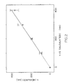
- Figure 2 illustrates the actual plating rate as determined by weight gain and profilometry in comparison to that calculated from Faraday's law using such preferred NiP and plating conditions.
- the horizontal axis, h (Q calculated) is the expected thickness of NiP based on Faraday's law.
- the vertical axis, h(measured), is the measured thickness.
- the "*" indicates measurement of the gain in weight of the NiP layer during the electroplating process.
- the vertical bars represent the range of values obtained by profilometry at different points on a plated sample.
- the solid line represents the theoretical curve for 100% efficient plating.
- the substrates were permalloy monitor wafers that were either blanket films or patterned with photoresist. From the data the current efficiency is calculated to be 100% +/-5% for NiP films of thickness greater than 1000 angstroms.
- the overall plating rate for the NiP deposition is 100 angstroms per 27 seconds or, equivalently, 15 plating pulses.
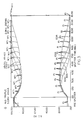
- Auger depth profiling was used to analyze for NiP deposits with thicknesses less than 1000 angstroms. Shown in Figure 3 are the profiles of NiP films of calculated thicknesses as indicated. The atomic % of Ni (upper curve) and atomic % of P (lower curve) in the NiP alloy layer is plotted against an ion sputter time (in minutes) that was used to etch the NiP alloy layer away. The lower phosphorous curves are plotted as atomic concentrations in percent while the upper nickel curves are normalized with respect to the phosphorous to total 100%. The concentration of phosphorous is about 18% and is independent of the thickness of the deposit within the accuracy of Auger.
- the sputter etching time of the NiP layer is indicative of the actual thickness and follows closely the calculated amount of NiP deposited.
- the exposed surface is represented at zero sputtering time.
- the consistent value of about 5% for the surface concentration of phosphorous is an artifact of the Auger and is due to the different escape depths of the Auger electrons for Ni and P.
- X-ray photoelectron spectroscopic measurements carried out on similar films have shown that the surface phosphorous concentration is actually somewhat higher than it is deeper into the film.
- Auger energy spectra have shown that the NiP layer and its interface with the permalloy substrate cannot detect any other elements.
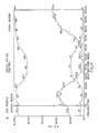
- Figure 4 shows the Auger depth profile of a 200 angstrom NiP layer electrodeposited on permalloy with a 100 angstrom evaporated permalloy overcoat.
- the graph plots the concentration of Ni, P and Fe in the laminate, versus the sputter time, in minutes. The P concentration is shown in atomic percent. The Fe peak height is arbitrarily scaled.
- the curve designated "NI1" is the nickel content curve
- the curve designated "P1” is the phosphorous content curve
- the curve designated "FE2" is the iron content curve.
- the NiP layer was first deposited on the NiFe substrate using the preferred bath and plating conditions described above. This sample was annealed for 20 hours at 265°C to test the effects of thermal cycling on diffusion.
- the phosphorous is scaled in atomic percent with the nickel again normalized to 100% as before.
- the iron curve is the Auger peak height arbitrarily scaled, where the maximum value corresponds to the permalloy concentration of 18%.
- the iron profile shows an effective lamination where the magnetic layers are separated by a region of approximately 18% atomic concentration of phosphorous.
- the small iron signal in the middle of the NiP layer is primarily due to the noise level of the Auger rather than the presence of iron or to pores in the NiP layer.
- the pore area here is estimated to be less than 0.1% of the plated surface.
- depth profiles of similar samples that were not annealed are essentially identical. Thus the amount of phosphorous diffusion out of the NiP layer is insignificant.
- NiP alloy with greater than 8% atomic phosphorous is non-magnetic (P. A. Albert, Z. Kovac, J. R. Lilienthal, T. A. McGuire, and Y. Nakamura, Journal of Applied Physics , Vol. 38, 1258, 1967). It is expected that about 10% of phosphorous in permalloy would quench its magnetic properties.
- Figures 5 to 8 are LAMOM Kerr magnetooptic magnetic domain images showing the wall movement under a varying applied magnetic field in inductive recording head yokes 1 and 2.
- Figures 7 and 8 are drawings showing the domains, walls and orientation of the corresponding images of Figures 5 and 6, respectively.
- the Figure 5 image is the result of the use of a permalloy film without lamination in head yoke 1.
- the structure contains many domains, as seen in Figure 7, whose walls are mobile under the influence of applied magnetic fields as would happen in a read operation.
- the domains of Figure 7 include triangular edge domains 3 and central domains 4. These domains are separated by domain walls 5.
- the arrows 6 represent the magnetic vectors for the respective domains.
- the image of Figure 6 is the result of the use of a permalloy layer of equal thickness with a single layer of 200 angstroms of NiP plated midway through the permalloy thickness in head yoke 2.
- the Figure 6 LAMOM image reveals the movement of only one major domain wall in the yoke 2 of the structure with some edge curling areas.
- edge domains 3 of Figure 7 are eliminated and are replaced by edge-curling walls depicted by arrows 7. Only one domain wall 8 remains in yoke 2.
- the edge curling walls 8 result from the rotation (curling) of the magnetic vector both in-plane and from one magnetic layer through the non-magnetic layer to the second magnetic layer.
- the domain structure of the laminated permalloy of Figure 8 is recognized as being less susceptible to Barkhausen noise (J. C. Slonczewski, B. Petek and B. E. Argyle, IEEE Transactions on Magnetics , Vol. 24, page 2045, 1988).
- Barkhausen noise J. C. Slonczewski, B. Petek and B. E. Argyle, IEEE Transactions on Magnetics , Vol. 24, page 2045, 1988.
- the Cr metal or CrNi alloy laminae of the present invention are also prepared from known techniques such as electrodeposition, sputtering, or vapor deposition on the magnetic laminae.
Landscapes
- Engineering & Computer Science (AREA)
- Chemical & Material Sciences (AREA)
- Crystallography & Structural Chemistry (AREA)
- Nanotechnology (AREA)
- Power Engineering (AREA)
- Manufacturing & Machinery (AREA)
- Magnetic Heads (AREA)
- Thin Magnetic Films (AREA)
Applications Claiming Priority (2)
| Application Number | Priority Date | Filing Date | Title |
|---|---|---|---|
| US477696 | 1983-03-22 | ||
| US07/477,696 US5576099A (en) | 1990-02-09 | 1990-02-09 | Inductive head lamination with layer of magnetic quenching material |
Publications (2)
| Publication Number | Publication Date |
|---|---|
| EP0441186A2 true EP0441186A2 (fr) | 1991-08-14 |
| EP0441186A3 EP0441186A3 (en) | 1992-07-08 |
Family
ID=23896971
Family Applications (1)
| Application Number | Title | Priority Date | Filing Date |
|---|---|---|---|
| EP19910100872 Withdrawn EP0441186A3 (en) | 1990-02-09 | 1991-01-24 | Magnetic film laminate and magnetic secondary head thereof |
Country Status (3)
| Country | Link |
|---|---|
| US (1) | US5576099A (fr) |
| EP (1) | EP0441186A3 (fr) |
| JP (1) | JPH04214203A (fr) |
Cited By (1)
| Publication number | Priority date | Publication date | Assignee | Title |
|---|---|---|---|---|
| EP0596448A3 (en) * | 1992-11-02 | 1995-12-13 | Matsushita Electric Industrial Co Ltd | Soft-magnetic multilayer thin film for use in a thin-film magnetic head and a method of manufacturing the same. |
Families Citing this family (11)
| Publication number | Priority date | Publication date | Assignee | Title |
|---|---|---|---|---|
| US6111724A (en) * | 1998-04-10 | 2000-08-29 | International Business Machines Corporation | Method of making a magnetic write head with plated self-aligned zero throat height defining layer without reflective notching of a second pole tip |
| US6259583B1 (en) | 1998-09-16 | 2001-07-10 | International Business Machines, Corporation | Laminated yoke head with a domain control element |
| US7037421B2 (en) * | 2000-05-19 | 2006-05-02 | Alps Electric Co., Ltd. | Thin-film magnetic head having magnetic gap formed of NiP |
| JP3708856B2 (ja) * | 2001-09-07 | 2005-10-19 | アルプス電気株式会社 | 軟磁性膜と前記軟磁性膜を用いた薄膜磁気ヘッド、および前記軟磁性膜の製造方法と前記薄膜磁気ヘッドの製造方法 |
| US7119988B2 (en) * | 2003-04-01 | 2006-10-10 | Hitachi Global Storage Technologies Netherlands, B.V. | Perpendicular magnetic head having modified shaping layer for direct plating of magnetic pole piece |
| US9495989B2 (en) | 2013-02-06 | 2016-11-15 | International Business Machines Corporation | Laminating magnetic cores for on-chip magnetic devices |
| US10784045B2 (en) | 2015-09-15 | 2020-09-22 | International Business Machines Corporation | Laminated magnetic materials for on-chip magnetic inductors/transformers |
| US10593449B2 (en) | 2017-03-30 | 2020-03-17 | International Business Machines Corporation | Magnetic inductor with multiple magnetic layer thicknesses |
| US10607759B2 (en) | 2017-03-31 | 2020-03-31 | International Business Machines Corporation | Method of fabricating a laminated stack of magnetic inductor |
| US10597769B2 (en) | 2017-04-05 | 2020-03-24 | International Business Machines Corporation | Method of fabricating a magnetic stack arrangement of a laminated magnetic inductor |
| US10347411B2 (en) | 2017-05-19 | 2019-07-09 | International Business Machines Corporation | Stress management scheme for fabricating thick magnetic films of an inductor yoke arrangement |
Family Cites Families (19)
| Publication number | Priority date | Publication date | Assignee | Title |
|---|---|---|---|---|
| NL269912A (fr) * | 1960-10-05 | |||
| US3303111A (en) * | 1963-08-12 | 1967-02-07 | Arthur L Peach | Electro-electroless plating method |
| US3634209A (en) * | 1969-07-15 | 1972-01-11 | Ampex | Electro deposited magnetic films |
| US3715793A (en) * | 1970-05-04 | 1973-02-13 | Honeywell Inc | Plated super-coat and electrolyte |
| US4108739A (en) * | 1973-09-04 | 1978-08-22 | Fuji Photo Film Co., Ltd. | Plating method for memory elements |
| DE2833249C2 (de) * | 1978-07-28 | 1985-05-09 | Siemens AG, 1000 Berlin und 8000 München | Verfahren zur Herstellung eines lamellierten Dünnschicht-Magnetkopfes mit mehreren Schichten aus abwechelnd magnetischem und unmagnetischem Material |
| JPS5771518A (en) * | 1980-10-22 | 1982-05-04 | Dainippon Printing Co Ltd | Magnetic recording medium |
| US4472248A (en) * | 1982-12-20 | 1984-09-18 | Minnesota Mining And Manufacturing Company | Method of making thin-film magnetic recording medium having perpendicular anisotropy |
| JPH061729B2 (ja) * | 1983-01-17 | 1994-01-05 | 株式会社日立製作所 | 磁性体膜およびそれを用いた磁気ヘッド |
| US4687712A (en) * | 1983-12-12 | 1987-08-18 | Matsushita Electric Industrial Co., Ltd. | Vertical magnetic recording medium |
| JPH0622170B2 (ja) * | 1983-12-16 | 1994-03-23 | 株式会社日立製作所 | 磁気ヘッド |
| JPS60258717A (ja) * | 1984-06-04 | 1985-12-20 | Nec Corp | 薄膜磁気ヘツドおよびその製造方法 |
| DE3685230D1 (de) * | 1985-02-15 | 1992-06-17 | Matsushita Electric Industrial Co Ltd | Magnetkopf. |
| JP2533860B2 (ja) * | 1986-09-24 | 1996-09-11 | 株式会社日立製作所 | 磁性超格子膜およびそれを用いた磁気ヘツド |
| US5108837A (en) * | 1987-12-04 | 1992-04-28 | Digital Equipment Corporation | Laminated poles for recording heads |
| JPH01238106A (ja) * | 1988-03-18 | 1989-09-22 | Nec Corp | 耐食性強磁性薄膜 |
| JPH01283907A (ja) * | 1988-05-11 | 1989-11-15 | Hitachi Ltd | 多層軟磁性膜とこれを用いた磁気ヘッドおよびトランス |
| US5032945A (en) * | 1989-11-07 | 1991-07-16 | International Business Machines Corp. | Magnetic thin film structures fabricated with edge closure layers |
| US5379172A (en) * | 1990-09-19 | 1995-01-03 | Seagate Technology, Inc. | Laminated leg for thin film magnetic transducer |
-
1990
- 1990-02-09 US US07/477,696 patent/US5576099A/en not_active Expired - Fee Related
-
1991
- 1991-01-24 EP EP19910100872 patent/EP0441186A3/en not_active Withdrawn
- 1991-02-07 JP JP3036669A patent/JPH04214203A/ja active Pending
Cited By (2)
| Publication number | Priority date | Publication date | Assignee | Title |
|---|---|---|---|---|
| EP0596448A3 (en) * | 1992-11-02 | 1995-12-13 | Matsushita Electric Industrial Co Ltd | Soft-magnetic multilayer thin film for use in a thin-film magnetic head and a method of manufacturing the same. |
| US5612146A (en) * | 1992-11-02 | 1997-03-18 | Matshushita Electric Industrial Co., Ltd. | Soft-magnetic multilayer thin film for use in a thin-film magnetic head and a method of manufacturing the same |
Also Published As
| Publication number | Publication date |
|---|---|
| EP0441186A3 (en) | 1992-07-08 |
| JPH04214203A (ja) | 1992-08-05 |
| US5576099A (en) | 1996-11-19 |
Similar Documents
| Publication | Publication Date | Title |
|---|---|---|
| Kawai et al. | Magnetic properties of anodic oxide coatings on aluminum containing electrodeposited Co and Co‐Ni | |
| US6855240B2 (en) | CoFe alloy film and process of making same | |
| JP3229718B2 (ja) | 軟磁性合金、軟磁性薄膜および多層膜 | |
| US5576099A (en) | Inductive head lamination with layer of magnetic quenching material | |
| CN100371989C (zh) | 软磁性薄膜和磁记录头 | |
| US7396445B2 (en) | Method of manufacturing a thin-film magnetic head using a soft magnetic film having high saturation magnetic flux density | |
| US6760189B2 (en) | Soft magnetic film having high corrosion resistance, magnetic head including the same, and method for making the soft magnetic film | |
| JP2002057030A (ja) | 軟磁性膜とこの軟磁性膜を用いた薄膜磁気ヘッド、ならびに前記軟磁性膜の製造方法と前記薄膜磁気ヘッドの製造方法 | |
| JP3102505B2 (ja) | 軟磁性多層めっき膜の製造方法および軟磁性多層めっき膜ならびに磁気ヘッド | |
| Vas’ ko et al. | High saturation magnetization films of FeCoCr | |
| Liu et al. | High moment FeCoNi alloy thin films fabricated by pulsed-current electrodeposition | |
| Khan et al. | Crystallographic and magnetic investigations of the cobalt columns electrodeposited in the pores of anodic alumina | |
| JPH06151171A (ja) | 軟磁性薄膜体とその製造方法およびそれを用いた磁気ヘッド | |
| EP0396227B1 (fr) | Dispositifs magnétiques avec pôles relevés | |
| JPS5870422A (ja) | 磁気記録用媒体の後処理法 | |
| US7095586B2 (en) | Soft magnetic film having saturation magnetic flux density Bs of at least 2.0 T and magnetic head including the same | |
| JP2502965B2 (ja) | 薄膜磁気ヘッド | |
| JP3431238B2 (ja) | 軟磁性めっき薄膜およびその製造方法 | |
| Lim et al. | Soft-solution process of Fe–Tb–O films for use in high frequency micromagnetic devices | |
| EP1821289A2 (fr) | Film mince magnétique doux, son procédé de fabrication et tête magnétique | |
| JPH0696949A (ja) | 磁性薄膜の製造方法 | |
| JP2003059717A (ja) | 軟磁性膜と薄膜磁気ヘッドとこれらの製造方法 | |
| Osaka et al. | Preparation of electrodeposited FeP films and their soft magnetic properties | |
| JP2897485B2 (ja) | 軟磁性薄膜およびその製造方法 | |
| JPH08236349A (ja) | 軟磁性薄膜およびそれを用いた薄膜磁気デバイス |
Legal Events
| Date | Code | Title | Description |
|---|---|---|---|
| PUAI | Public reference made under article 153(3) epc to a published international application that has entered the european phase |
Free format text: ORIGINAL CODE: 0009012 |
|
| AK | Designated contracting states |
Kind code of ref document: A2 Designated state(s): DE FR GB |
|
| 17P | Request for examination filed |
Effective date: 19911211 |
|
| PUAL | Search report despatched |
Free format text: ORIGINAL CODE: 0009013 |
|
| AK | Designated contracting states |
Kind code of ref document: A3 Designated state(s): DE FR GB |
|
| 17Q | First examination report despatched |
Effective date: 19931118 |
|
| GRAG | Despatch of communication of intention to grant |
Free format text: ORIGINAL CODE: EPIDOS AGRA |
|
| STAA | Information on the status of an ep patent application or granted ep patent |
Free format text: STATUS: THE APPLICATION IS DEEMED TO BE WITHDRAWN |
|
| 18D | Application deemed to be withdrawn |
Effective date: 19960801 |