EP0442064A1 - Structure de protection d'entrée pour circuits intégrés - Google Patents
Structure de protection d'entrée pour circuits intégrés Download PDFInfo
- Publication number
- EP0442064A1 EP0442064A1 EP90123222A EP90123222A EP0442064A1 EP 0442064 A1 EP0442064 A1 EP 0442064A1 EP 90123222 A EP90123222 A EP 90123222A EP 90123222 A EP90123222 A EP 90123222A EP 0442064 A1 EP0442064 A1 EP 0442064A1
- Authority
- EP
- European Patent Office
- Prior art keywords
- base
- emitter
- collector
- protection structure
- transistor
- Prior art date
- Legal status (The legal status is an assumption and is not a legal conclusion. Google has not performed a legal analysis and makes no representation as to the accuracy of the status listed.)
- Granted
Links
- 239000004065 semiconductor Substances 0.000 claims abstract description 17
- 239000000758 substrate Substances 0.000 claims abstract description 13
- 238000009413 insulation Methods 0.000 claims description 9
- 230000001681 protective effect Effects 0.000 description 10
- 238000002955 isolation Methods 0.000 description 4
- 230000015556 catabolic process Effects 0.000 description 3
- 238000009795 derivation Methods 0.000 description 3
- 230000004888 barrier function Effects 0.000 description 2
- 239000004020 conductor Substances 0.000 description 2
- 230000006378 damage Effects 0.000 description 2
- 230000007704 transition Effects 0.000 description 2
- 102000003712 Complement factor B Human genes 0.000 description 1
- 108090000056 Complement factor B Proteins 0.000 description 1
- VYPSYNLAJGMNEJ-UHFFFAOYSA-N Silicium dioxide Chemical compound O=[Si]=O VYPSYNLAJGMNEJ-UHFFFAOYSA-N 0.000 description 1
- 238000007796 conventional method Methods 0.000 description 1
- 230000001419 dependent effect Effects 0.000 description 1
- 230000001066 destructive effect Effects 0.000 description 1
- 238000011161 development Methods 0.000 description 1
- 230000018109 developmental process Effects 0.000 description 1
- 238000010586 diagram Methods 0.000 description 1
- 238000000265 homogenisation Methods 0.000 description 1
- 238000002513 implantation Methods 0.000 description 1
- 238000004519 manufacturing process Methods 0.000 description 1
- 238000000034 method Methods 0.000 description 1
- 230000008092 positive effect Effects 0.000 description 1
- 229910052710 silicon Inorganic materials 0.000 description 1
- 239000010703 silicon Substances 0.000 description 1
- 229910052814 silicon oxide Inorganic materials 0.000 description 1
Images

Classifications
-
- H—ELECTRICITY
- H10—SEMICONDUCTOR DEVICES; ELECTRIC SOLID-STATE DEVICES NOT OTHERWISE PROVIDED FOR
- H10D—INORGANIC ELECTRIC SEMICONDUCTOR DEVICES
- H10D89/00—Aspects of integrated devices not covered by groups H10D84/00 - H10D88/00
- H10D89/60—Integrated devices comprising arrangements for electrical or thermal protection, e.g. protection circuits against electrostatic discharge [ESD]
Definitions
- the present invention relates to an input protection structure for integrated circuits, which is arranged in a semiconductor substrate and contains at least one transistor and an integrated diode.
- Integrated circuits require reliable protection against electrostatic discharge. For this purpose they are provided with entrance protection structures, some structures corresponding to the state of the art are explained in DE-OS 36 16 394.
- the present invention has for its object to provide an input protection structure for integrated circuits, which enables fast and reliable protection against electrostatic discharges of both polarities.
- the 1 lies between an input connection 1 of an integrated circuit, in particular a bipolar integrated circuit, and a connection for a reference potential 2, in particular a ground connection, a protective structure which is formed by a transistor 3 and a diode 4 connected in parallel with the collector-emitter path of the transistor.
- the collector 11, 12a of the transistor 3 and a pole 11 of the diode 4 are connected to the input 1, the emitter 16 of the transistor 3 and the other pole 10 of the diode 4 can be connected to the reference potential 2.
- the base 15 of the transistor 3 has no external connection (floating base), it only has contact with the collector 11, 12a and the emitter 16.
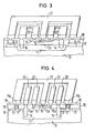
- FIGS. 2 to 4 show three exemplary embodiments of the implementation of the protective structure according to FIG. 1 in a semiconductor system; a sectional image with additional oblique view to the rear is used.
- the reference symbols are chosen in accordance with FIG. 1.
- a semiconductor substrate 10 of a first conductivity type preferably of the p-conductivity type and consisting of silicon
- an epitaxial layer 12 of the opposite second conductivity type preferably of the n-conductivity type
- all the exemplary embodiments have in common a buried zone 11 of the second conductivity type, which, like the other doped zones to be explained below, can be produced by means of conventional methods, for example implantation with a subsequent temperature step.
- an insulation frame 13 consisting of doped zones of the first conductivity type, is used to isolate the entire protective structure from neighboring components (pn insulation).
- This closed insulation frame 13 separates an inner region 12a of the epitaxial layer 12 from the rest of the outer epitaxial layer 12. Together with the buried zone 11, the partial region 12a forms the collector of the transistor 3 and is covered by a particularly heavily doped zone 14 thereof Line type, which preferably, but not necessarily, extends into the buried zone 11.
- a doped zone 15 of the first conductivity type which represents the base of the transistor 3, and within this in turn there is a doped zone 16 of the second conductivity type as the emitter of the transistor 3.
- the previously described doped zones are arranged essentially centrally symmetrically that is, the heavily doped zone 14 is located approximately in the middle of the partial region 12a, the zones 15 and 16 lie in a frame-like manner around the heavily doped zone 14.
- the buried zone 11 is preferably dimensioned such that it completely covers the area enclosed by the base-emitter ring 15, 16.
- the insulation frame 13 is arranged around this entire protective structure.
- the surface of the semiconductor system is covered with an insulating layer 18, which has either arisen in the preceding temperature steps or has been applied separately and preferably consists of silicon oxide.
- the highly doped zone 14 can be connected to a conductor track 20, and there is also a preferably annular opening in it above the likewise ring-shaped zone 16, which serves as an emitter. Through it, the emitter 16 can be connected to the reference potential 2 via a conductor track 21 be connected.
- the zone 15 forming the base is completely covered on the surface by the insulating layer 18.
- the semiconductor substrate 10 has a ground connection outside the protective structure, so that the integrated diode 4 is formed by the buried zone 11 and the semiconductor substrate 10.
- the second embodiment according to FIG. 3 can also be used for pn isolation of adjacent components (isolation frame 13) and essentially corresponds to the first embodiment.
- an npn standard component is used for the transistor 3, which results in a more strip-shaped structure.
- the emitter 16 is arranged in the middle, the interconnect 21 contacting it serves at the same time for connecting the semiconductor substrate 10 via the insulation frame 13 to the reference potential 2.
- the base 15 of the transistor 3 is essentially arranged symmetrically to the emitter 16 and, as in FIG. 3, can be connected to interconnects 22 by two correspondingly symmetrically arranged openings in the insulating layer 18.
- these two interconnects 22 are not connected to the outside, but are advantageously connected to one another; they ensure a homogeneous potential distribution in the base area, but are not absolutely necessary.
- the collector formed from buried zone 11 and partial region 12a of the epitaxial layer 12 has two connections which are arranged essentially symmetrically to the emitter 16 and consist of the highly doped zones 14 which do not necessarily extend into the buried zone 11. It is connected to input 1 via the interconnects 20.
- the integrated diode 4 is formed by the buried zone 11 and the semiconductor substrate 10, which is connected to the reference potential 2 together with the emitter 16 via the insulation frame 13 and the interconnect 21.
- FIG. 4 shows an embodiment of the invention in the case of oxide isolation of adjacent components using a standard npn transistor.
- the transistor 3 is configured essentially as in the second exemplary embodiment, the base 15 has two additional highly doped base contact zones 15a for connection to the interconnects 22.
- channel stopper regions 17 serve here at the same time to connect the semiconductor substrate 10 to the surface of the semiconductor system, where they make contact with the interconnect 21 and a highly doped zone 15b, which was produced simultaneously with the base contact zone 15a and therefore also the first Has line type. In this way, the semiconductor substrate 10 can be connected to the reference potential 2 together with the emitter 16 will.
- the integrated diode 4 is formed by the buried zone 11 and the semiconductor substrate 10, by means of the interconnects 20 and 21 it is connected between the input and the reference potential.
- Negative voltages at input 1 are derived to reference potential 2 via diode 4 integrated in the protective structure.
- the sensitive base-emitter junction is polarized in the reverse direction, the centrally symmetrical structure of FIG. 2 being of great advantage. Due to the ring-shaped, extensive barrier layer, the load is distributed over a larger area of the emitter-base junction, which compensates for the disadvantage of the sole discharge path across the diode path. For this reason, the centrally symmetrical structure of FIG. 2 ensures a load capacity or protective effect of the order of many thousands of volts which is equally high for both voltage polarities, although the derivation of positive pulses (see below) is inherently due to the transistor mode of operation which prevails in this case is favored.
- transistor 3 When there are positive pulses at input 1, transistor 3 is in the normal operating range, so that the sensitive emitter-base transition is only slightly loaded. Since the base 15 is not connected, the pulse is derived via a U CEO breakthrough.
- the early avalanche breakthrough favors the non-destructive derivation of the impulse.
- the centrally symmetrical structure of FIG. 2 also has a positive effect here, the large emitter area 16 causing an increase in the emitter effectiveness and thus the derivation favored by the impulse.
- the large emitter area does not result in a disadvantage in terms of increasing the additional capacitance, since only the transitions between the epitaxial layer and the base region and the buried zone 11 and substrate 10, ie between regions with relatively weak doping, are decisive for positive signal voltages.
- FIG. 2 For integrated circuits with pn isolation, the use of the structure of FIG. 2 is appropriate due to the considerations set out above, which, in addition to the advantages of a small space requirement, a small additional capacitance and an equally excellent protective effect for both voltage polarities, only has the disadvantage of one of the base area not connected has increased reverse current.
- the more homogeneous potential distribution generated due to the interconnects 22 contacting the base 15 within the base region reduces the occurrence of local junction breakdowns, which can lead to destruction due to the spatially limited power.
- a symmetrical structure in accordance with FIG. 4 is expedient, although one generally does not have to reckon with the disadvantage of increased reverse currents.
- two highly doped base contact zones 15a which are arranged symmetrically to the emitter, are advantageously used, which together with their interconnects 22 (not connected) contribute to the homogenization of the potential distribution in the base zone 15 (generally weakly doped).
- the base contact zones 15a reduce the expansion of the barrier layer between the epitaxial layer and the base region (both regions are generally weakly doped) with positive impulses, as a result of which an avalanche breakdown leads to destruction only when high voltages are present.
Landscapes
- Bipolar Integrated Circuits (AREA)
- Bipolar Transistors (AREA)
- Semiconductor Integrated Circuits (AREA)
Applications Claiming Priority (2)
| Application Number | Priority Date | Filing Date | Title |
|---|---|---|---|
| DE4004752 | 1990-02-15 | ||
| DE4004752 | 1990-02-15 |
Publications (2)
| Publication Number | Publication Date |
|---|---|
| EP0442064A1 true EP0442064A1 (fr) | 1991-08-21 |
| EP0442064B1 EP0442064B1 (fr) | 1996-03-27 |
Family
ID=6400250
Family Applications (1)
| Application Number | Title | Priority Date | Filing Date |
|---|---|---|---|
| EP90123222A Expired - Lifetime EP0442064B1 (fr) | 1990-02-15 | 1990-12-04 | Structure de protection d'entrée pour circuits intégrés |
Country Status (3)
| Country | Link |
|---|---|
| EP (1) | EP0442064B1 (fr) |
| JP (1) | JPH04214662A (fr) |
| DE (1) | DE59010248D1 (fr) |
Cited By (1)
| Publication number | Priority date | Publication date | Assignee | Title |
|---|---|---|---|---|
| EP0800273A3 (fr) * | 1996-04-01 | 1999-01-13 | Motorola, Inc. | Commande d'inductance et procédé y afférent |
Families Citing this family (1)
| Publication number | Priority date | Publication date | Assignee | Title |
|---|---|---|---|---|
| JP4775682B2 (ja) * | 2003-09-29 | 2011-09-21 | オンセミコンダクター・トレーディング・リミテッド | 半導体集積回路装置 |
Citations (4)
| Publication number | Priority date | Publication date | Assignee | Title |
|---|---|---|---|---|
| US4017882A (en) * | 1975-12-15 | 1977-04-12 | Rca Corporation | Transistor having integrated protection |
| FR2335055A1 (fr) * | 1975-12-09 | 1977-07-08 | Radiotechnique Compelec | Dispositif semi-conducteur integre comportant une diode de protection contre les surtensions, et procede de fabrication d'un tel dispositif |
| US4291319A (en) * | 1976-05-19 | 1981-09-22 | National Semiconductor Corporation | Open base bipolar transistor protective device |
| GB2176053A (en) * | 1985-05-30 | 1986-12-10 | Sgs Microelettronica Spa | Device for protection against electrostatic discharges for bipolar integrated circuits |
-
1990
- 1990-12-04 EP EP90123222A patent/EP0442064B1/fr not_active Expired - Lifetime
- 1990-12-04 DE DE59010248T patent/DE59010248D1/de not_active Expired - Fee Related
-
1991
- 1991-02-13 JP JP3041311A patent/JPH04214662A/ja active Pending
Patent Citations (4)
| Publication number | Priority date | Publication date | Assignee | Title |
|---|---|---|---|---|
| FR2335055A1 (fr) * | 1975-12-09 | 1977-07-08 | Radiotechnique Compelec | Dispositif semi-conducteur integre comportant une diode de protection contre les surtensions, et procede de fabrication d'un tel dispositif |
| US4017882A (en) * | 1975-12-15 | 1977-04-12 | Rca Corporation | Transistor having integrated protection |
| US4291319A (en) * | 1976-05-19 | 1981-09-22 | National Semiconductor Corporation | Open base bipolar transistor protective device |
| GB2176053A (en) * | 1985-05-30 | 1986-12-10 | Sgs Microelettronica Spa | Device for protection against electrostatic discharges for bipolar integrated circuits |
Non-Patent Citations (3)
| Title |
|---|
| IBM TECHNICAL DISCLOSURE BULLETIN. vol. 27, no. 3, August 1984, NEW YORK US Seiten 1570 - 1571; J. R. CAVALIERE et al.: "ELECTROSTATIC DISCHARGE PROTECTION DEVICE IN DEEP TRENCH ISOLATION STRUCTURE" * |
| PATENT ABSTRACTS OF JAPAN vol. 10, no. 91 (E-394)(2148) 09 April 1986, & JP-A-60 235452 (SANYO DENKI) 22 November 1985, * |
| PATENT ABSTRACTS OF JAPAN vol. 7, no. 174 (E-190)(1319) 02 August 1983, & JP-A-58 79744 (NIPPON DENKI) 13 Mai 1983, * |
Cited By (1)
| Publication number | Priority date | Publication date | Assignee | Title |
|---|---|---|---|---|
| EP0800273A3 (fr) * | 1996-04-01 | 1999-01-13 | Motorola, Inc. | Commande d'inductance et procédé y afférent |
Also Published As
| Publication number | Publication date |
|---|---|
| DE59010248D1 (de) | 1996-05-02 |
| EP0442064B1 (fr) | 1996-03-27 |
| JPH04214662A (ja) | 1992-08-05 |
Similar Documents
| Publication | Publication Date | Title |
|---|---|---|
| EP1019964B1 (fr) | Circuit integre a semiconducteur comportant une structure servant a la protection contre des decharges electrostatiques | |
| DE19518549C2 (de) | MOS-Transistor getriggerte Schutzschaltung gegen elektrostatische Überspannungen von CMOS-Schaltungen | |
| DE69226337T2 (de) | Schutzstruktur gegen elektrostatische Entladungen | |
| DE3834841C2 (de) | Integrierte Anordnung in einem Substrat zur Vermeidung parasitärer Substrateffekte | |
| DE19654163B4 (de) | Schutzvorrichtung für eine Halbleiterschaltung | |
| DE69527146T2 (de) | Integriertes MOS-Bauelement mit einer Gateschutzdiode | |
| DE2257846B2 (de) | Integrierte Halbleiteranordnung zum Schutz gegen Überspannung | |
| EP0905782B1 (fr) | Circuit intégré semi-conducteur comprenant des moyens de protection contre des décharges électrostatiques | |
| EP0538507B1 (fr) | Circuit de protection pour contacts de connexion de circuits intégrés monolithiques | |
| DE69121615T2 (de) | Schaltungsanordnung zur Verhinderung des Latch-up-Phänomens in vertikalen PNP-Transistoren mit isoliertem Kollektor | |
| DE68916192T2 (de) | Ausgangspuffer einer integrierten Schaltung mit einem verbesserten ESD-Schutz. | |
| DE2030423A1 (de) | Integrierte Metall Oxid Halbleiter schaltung mit einer Schutzschaltung gegen Spannungsstoßc | |
| EP0000169A1 (fr) | Condensateur à jonction semiconducteur dans un mode intégré de construction et circuit du type bootstrap avec un tel condensateur | |
| DE2539967C2 (de) | Logikgrundschaltung | |
| EP1128442A2 (fr) | Sructure de thyristor latéral pour protetion contre les décharges électrostatiques | |
| EP1127377B1 (fr) | Transistor de securite a dissipation electrostatique | |
| EP0442064B1 (fr) | Structure de protection d'entrée pour circuits intégrés | |
| EP0656659B1 (fr) | Structure de protection ESD pour circuit intégrés | |
| EP0413054B1 (fr) | Structure de protection d'entrée pour circuits intégrés | |
| EP0477393B1 (fr) | Structure de protection d'entrée pour circuits intégrés | |
| EP0379199B1 (fr) | Structure de protection ESD | |
| EP0429686B1 (fr) | Structure de protection d'entrée pour circuits intégrés | |
| EP0414934B1 (fr) | Structure de protection d'entrée pour circuits intégrés | |
| DE10111462A1 (de) | Thyristorstruktur und Überspannungsschutzanordnung mit einer solchen Thyristorstruktur | |
| DE4219019B4 (de) | MOS-Halbleiterbauelement |
Legal Events
| Date | Code | Title | Description |
|---|---|---|---|
| PUAI | Public reference made under article 153(3) epc to a published international application that has entered the european phase |
Free format text: ORIGINAL CODE: 0009012 |
|
| 17P | Request for examination filed |
Effective date: 19901220 |
|
| AK | Designated contracting states |
Kind code of ref document: A1 Designated state(s): DE FR GB IT NL |
|
| 17Q | First examination report despatched |
Effective date: 19931007 |
|
| GRAA | (expected) grant |
Free format text: ORIGINAL CODE: 0009210 |
|
| AK | Designated contracting states |
Kind code of ref document: B1 Designated state(s): DE FR GB IT NL |
|
| REF | Corresponds to: |
Ref document number: 59010248 Country of ref document: DE Date of ref document: 19960502 |
|
| ITF | It: translation for a ep patent filed | ||
| GBT | Gb: translation of ep patent filed (gb section 77(6)(a)/1977) |
Effective date: 19960531 |
|
| ET | Fr: translation filed | ||
| PLBE | No opposition filed within time limit |
Free format text: ORIGINAL CODE: 0009261 |
|
| STAA | Information on the status of an ep patent application or granted ep patent |
Free format text: STATUS: NO OPPOSITION FILED WITHIN TIME LIMIT |
|
| 26N | No opposition filed | ||
| PGFP | Annual fee paid to national office [announced via postgrant information from national office to epo] |
Ref country code: DE Payment date: 20010219 Year of fee payment: 11 |
|
| PGFP | Annual fee paid to national office [announced via postgrant information from national office to epo] |
Ref country code: FR Payment date: 20011204 Year of fee payment: 12 |
|
| PGFP | Annual fee paid to national office [announced via postgrant information from national office to epo] |
Ref country code: NL Payment date: 20011206 Year of fee payment: 12 Ref country code: GB Payment date: 20011206 Year of fee payment: 12 |
|
| REG | Reference to a national code |
Ref country code: GB Ref legal event code: IF02 |
|
| PG25 | Lapsed in a contracting state [announced via postgrant information from national office to epo] |
Ref country code: DE Free format text: LAPSE BECAUSE OF NON-PAYMENT OF DUE FEES Effective date: 20020702 |
|
| PG25 | Lapsed in a contracting state [announced via postgrant information from national office to epo] |
Ref country code: GB Free format text: LAPSE BECAUSE OF NON-PAYMENT OF DUE FEES Effective date: 20021204 |
|
| PG25 | Lapsed in a contracting state [announced via postgrant information from national office to epo] |
Ref country code: NL Free format text: LAPSE BECAUSE OF NON-PAYMENT OF DUE FEES Effective date: 20030701 |
|
| GBPC | Gb: european patent ceased through non-payment of renewal fee | ||
| NLV4 | Nl: lapsed or anulled due to non-payment of the annual fee |
Effective date: 20030701 |
|
| PG25 | Lapsed in a contracting state [announced via postgrant information from national office to epo] |
Ref country code: FR Free format text: LAPSE BECAUSE OF NON-PAYMENT OF DUE FEES Effective date: 20030901 |
|
| REG | Reference to a national code |
Ref country code: FR Ref legal event code: ST |
|
| PG25 | Lapsed in a contracting state [announced via postgrant information from national office to epo] |
Ref country code: IT Free format text: LAPSE BECAUSE OF NON-PAYMENT OF DUE FEES;WARNING: LAPSES OF ITALIAN PATENTS WITH EFFECTIVE DATE BEFORE 2007 MAY HAVE OCCURRED AT ANY TIME BEFORE 2007. THE CORRECT EFFECTIVE DATE MAY BE DIFFERENT FROM THE ONE RECORDED. Effective date: 20051204 |