EP0442491A2 - Dispositif semi-conducteur comprenant une configuration de conducteurs dans laquelle une pluralité de lignes sont arrangeés d'une façon très serrée - Google Patents
Dispositif semi-conducteur comprenant une configuration de conducteurs dans laquelle une pluralité de lignes sont arrangeés d'une façon très serrée Download PDFInfo
- Publication number
- EP0442491A2 EP0442491A2 EP91102091A EP91102091A EP0442491A2 EP 0442491 A2 EP0442491 A2 EP 0442491A2 EP 91102091 A EP91102091 A EP 91102091A EP 91102091 A EP91102091 A EP 91102091A EP 0442491 A2 EP0442491 A2 EP 0442491A2
- Authority
- EP
- European Patent Office
- Prior art keywords
- lines
- semiconductor device
- intervals
- patterned
- patterned lines
- Prior art date
- Legal status (The legal status is an assumption and is not a legal conclusion. Google has not performed a legal analysis and makes no representation as to the accuracy of the status listed.)
- Granted
Links
Images


Classifications
-
- H—ELECTRICITY
- H10—SEMICONDUCTOR DEVICES; ELECTRIC SOLID-STATE DEVICES NOT OTHERWISE PROVIDED FOR
- H10W—GENERIC PACKAGES, INTERCONNECTIONS, CONNECTORS OR OTHER CONSTRUCTIONAL DETAILS OF DEVICES COVERED BY CLASS H10
- H10W20/00—Interconnections in chips, wafers or substrates
- H10W20/40—Interconnections external to wafers or substrates, e.g. back-end-of-line [BEOL] metallisations or vias connecting to gate electrodes
- H10W20/41—Interconnections external to wafers or substrates, e.g. back-end-of-line [BEOL] metallisations or vias connecting to gate electrodes characterised by their conductive parts
- H10W20/435—Cross-sectional shapes or dispositions of interconnections
-
- H—ELECTRICITY
- H10—SEMICONDUCTOR DEVICES; ELECTRIC SOLID-STATE DEVICES NOT OTHERWISE PROVIDED FOR
- H10W—GENERIC PACKAGES, INTERCONNECTIONS, CONNECTORS OR OTHER CONSTRUCTIONAL DETAILS OF DEVICES COVERED BY CLASS H10
- H10W20/00—Interconnections in chips, wafers or substrates
- H10W20/40—Interconnections external to wafers or substrates, e.g. back-end-of-line [BEOL] metallisations or vias connecting to gate electrodes
- H10W20/41—Interconnections external to wafers or substrates, e.g. back-end-of-line [BEOL] metallisations or vias connecting to gate electrodes characterised by their conductive parts
- H10W20/43—Layouts of interconnections
Definitions
- This invention relates to a semiconductor device having a plurality of lines arranged in close proximity to one another, and more particularly to a semiconductor device having a fine line pattern.
- a plurality of patterned lines are arranged at minimum intervals, before and after they are bent at their bending portions.
- the interval between adjacent lines is the same in any portion of the line pattern.
- a CVD oxide film is formed on the entire line pattern, except for the bonding pads, to protect the surface of the chip. More specifically, after the line pattern is formed, a CVD oxide film is deposited on the chip and openings are then formed in desired portions of the CVD film by means of the following steps: a CVD film depositing step, a cleaning step, a drying step, a resist applying step, a resist pre-baking step, a pattern printing step, a developing step, and a CVD film etching step, or the like.
- a liquid used in the succeeding cleaning step or the like tends to fill the pores in the bending portion of the line pattern due to the capillary phenomenon.
- the liquid which fills the pores does not dry sufficiently in the drying step and remains in the bending portion. Then, as the liquid is vaporized in the resist pre-baking step, the resist film which has been applied to the CVD film explodes, thereby forming a hole. Consequently, a portion which should have been covered by the resist film is exposed, and undesirable etching is performed on that portion, resulting in a defective device.
- the pores in the CVD film are not filled with liquid, they may fill with gas, in which case, the gas will expand in the resist pre-baking step, again forming a hole.
- a semiconductor device comprising: a plurality of first patterned lines extending in one direction on an insulation layer and arranged at first intervals; a plurality of second patterned lines, whose ends are respectively connected to the ends of the first patterned lines and which extend along lines crossing the first patterned lines and arranged at second intervals which are wider than the first intervals; and a CVD oxide film deposited on the entire surface of the insulation layer, including the first and second lines.
- a semiconductor device comprising: a plurality of first patterned lines extending in one direction on an insulation layer and arranged at first intervals, each of the first patterned lines having a first width; a plurality of second patterned lines, whose end portions are respectively connected to the end portions of the first patterned lines and which extend along lines crossing the first patterned lines and arranged at the second intervals, each of the second patterned lines having a second width; and a CVD oxide film deposited on the entire surface of the insulation layer including the first and second lines.
- a semiconductor device comprising: a plurality of first patterned lines extending in one direction on an insulation layer and arranged at minimum intervals according to design rules of the semiconductor device, each of the first patterned lines having a predetermined thickness; a plurality of second patterned lines, whose end portions are respectively connected to the end portions of the first patterned lines, extending along lines crossing the first patterned lines and arranged at minimum intervals according to the design rules of the semiconductor device, each of the second patterned lines having another predetermined thickness; and a CVD oxide film deposited on the entire surface of the insulation layer, including the first and second lines.
- a plurality of patterned lines are arranged at minimum intervals, before and after they are bent at their bending portions.
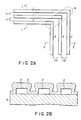
- Fig. 1A three lines 1, 1, 1, which are made of aluminum or the like and extend in a horizontal direction, are arranged at minimum intervals ⁇ 1 according to design rules.
- Three other lines 2, 2, 2 made of aluminum or the like extend perpendicular to the lines 1, 1, 1, and are connected to the end portions of the lines 1, 1, 1.
- the lines 2, 2, 2 are also arranged at minimum intervals.
- the lines 1, 1, 1 and 2, 2, 2 have minimum widths according to the design rules.
- a CVD oxide film is formed on the entire line pattern to protect the surface of the chip. More specifically, after the line pattern is formed, a CVD oxide film is deposited on the chip and openings are then formed in desired portions of the CVD film by means of the following steps: a CVD film depositing step, a cleaning step, a drying step, a resist applying step, a resist pre-baking step, a pattern printing step, a developing step, and a CVD film etching step, or the like.
- Fig. 1B shows a state in which pores 4 are formed in the CVD oxide film 3.
- the lines 1, 1, 1 and 2, 2, 2 are formed on an insulation film 5.
- pores 4 are formed in the CVD oxide film 3 as described above, a liquid used in the succeeding cleaning step or the like tends to fill the pores in the bending portion of the line pattern due to the capillary phenomenon.
- the liquid which fills the pores does not dry sufficiently in the drying step and remains especially in the bending portion. Then, as the liquid is vaporized in the resist pre-baking step, the resist film which has been applied to the CVD film explodes, thereby forming a hole. Consequently, a portion which should have been covered by the resist film is exposed, and undesirable etching is performed on that portion, resulting in a defective device.
- first patterned lines 1, 1, 1, made of aluminum or the like and extending in a horizontal direction in the drawing are arranged at minimum intervals ⁇ 1 according to design rules.
- Three second patterned lines 2, 2, 2, made of aluminum or the like, extend perpendicular to the lines 1, 1, 1, and their end portions are respectively connected to the end portions of the lines 1, 1, 1.
- the lines 2, 2, 2 are arranged at intervals ⁇ 2 which are wider than the minimum intervals ⁇ 1. All of the lines 1, 1, 1 and 2, 2, 2 have minimum widths within the limits of their design rules.
- Fig. 2B shows a cross section of the line pattern taken along the line II-II of Fig. 2A.
- the cross section taken along the line I-I is the same as that shown in Fig. 1B.
- a CVD oxide film 3 is deposited on the lines 1, 1, 1 and 2, 2, 2, which are formed on an insulation film 5.
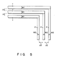
- Fig. 3 shows a semiconductor device according to a second embodiment of the present invention.
- intermediate lines 6, 6, 6 connect two sets of patterned lines 1, 1, 1 and 2, 2, 2, which are arranged at right angles to each other, in contrast to the first embodiment in which the first patterned lines 1, 1, 1 are directly connected to the second patterned lines 2, 2, 2.
- two lines are allowed to form an angle of 90°C or 135°C.
- the second embodiment corresponds to the case in which two lines form an angle of 135°C.
- the present invention can be applied to a device in which lines bend at desired angles.
- the interval ⁇ 2 between the second patterned lines 2, 2 is wider than the interval ⁇ 1 between the first patterned lines 1, 1, explosion of the resist film due to vaporization of the liquid in the pre-baking step is prevented, and therefore no holes are formed in the resist film.
- Fig. 4 is a sectional view of the line pattern at a portion where the lines are arranged at intervals ⁇ (corresponding to ⁇ 2) which is wider than the minimum interval ⁇ 1.
- the CVD film 3, formed on the lines 2 made of aluminum, has a thickness of T1.
- the thickness T2 of the overhanging portion on the shoulder of the line 2 is about 0.9 ⁇ T1.
- the distance T3 between the edge of the bottom surface of the stepped portion of the CVD film 3 and the edge of the line 2 is about 0.8 ⁇ T1. Pores are formed in the CVD film 3 due to the fact that the thickness T3 is smaller than the thickness T2. If the lines 2, 2, 2 are parallel to one another, an overhanging portion of the CVD film 3 formed on a line 2 faces close to that formed on an adjacent line 2.
- a distance T4 obtained by subtracting 2 ⁇ T2 (the thicknesses of the overhanging portions formed on both shoulders of a line 2) from ⁇ (the distance between two adjacent lines) reduces in reverse proportion to T1 (the thickness of the CVD film 3). If T4 is 0, a pore is formed in the CVD film 3 between the two adjacent lines, when ⁇ is 1.8 ⁇ T1 or less.
- the lines 2, 2, 2 are arranged at intervals of 1.62 ⁇ m or longer, e.g., 1.8 ⁇ m.
- first patterned lines 1, 1, 1 have a width W1, which is wider than the minimum width according to design rules
- second patterned lines 2, 2, 2 have a width W2, which is the minimum width according to the design rules.
- An interval between adjacent lines 1, 1, 1 is ⁇ 1, which is the minimum interval within the limits of design rules.
- Ah interval between adjacent lines 2, 2, 2 is ⁇ 2, which is wider than ⁇ 1.
- second patterned lines 2, 2, 2 are thinner than first patterned lines 1, 1, 1. All of the lines 1, 1, 1 and 2, 2, 2 have the minimum width according to design rules and arranged at intervals ⁇ 1, which is the minimum interval according to the design rules. No pores are formed in the CVD film 3 as shown in Fig. 6B, because one set of lines is thinner than the other sets of lines extending perpendicular thereto. Hence, explosion of the resist film due to vaporization of liquid filling pores does not occur in the pre-baking step, and therefore no hole is formed in the resist film.
- lines 2, 2, 2 are arranged at regular intervals of ⁇ 2 in the above embodiments, the intervals need not be the same, so long as they are longer than ⁇ 1.
- lines need not be made of aluminum, but can be made of tungstem, cuprum, polycrystalline silicon, or the like.
- a semiconductor device in which a CVD oxide film is deposited on a line pattern having a plurality of lines arranged at predetermined intervals and a bending portion, wherein no liquid remains in the bending portion and undesirable etching of the CVD oxide film at the bending portion of the line pattern is prevented.
Landscapes
- Internal Circuitry In Semiconductor Integrated Circuit Devices (AREA)
- Electrodes Of Semiconductors (AREA)
Applications Claiming Priority (2)
| Application Number | Priority Date | Filing Date | Title |
|---|---|---|---|
| JP2031488A JPH06105710B2 (ja) | 1990-02-14 | 1990-02-14 | 半導体装置 |
| JP31488/90 | 1990-02-14 |
Publications (3)
| Publication Number | Publication Date |
|---|---|
| EP0442491A2 true EP0442491A2 (fr) | 1991-08-21 |
| EP0442491A3 EP0442491A3 (en) | 1991-11-13 |
| EP0442491B1 EP0442491B1 (fr) | 1995-11-15 |
Family
ID=12332657
Family Applications (1)
| Application Number | Title | Priority Date | Filing Date |
|---|---|---|---|
| EP91102091A Expired - Lifetime EP0442491B1 (fr) | 1990-02-14 | 1991-02-14 | Dispositif semi-conducteur comprenant une configuration de conducteurs dans laquelle une pluralité de lignes sont arrangeés d'une façon très serrée |
Country Status (4)
| Country | Link |
|---|---|
| EP (1) | EP0442491B1 (fr) |
| JP (1) | JPH06105710B2 (fr) |
| KR (1) | KR930009017B1 (fr) |
| DE (1) | DE69114539T2 (fr) |
Cited By (4)
| Publication number | Priority date | Publication date | Assignee | Title |
|---|---|---|---|---|
| DE19530951A1 (de) * | 1995-08-23 | 1997-02-27 | Bosch Gmbh Robert | Verfahren zur Anordnung von Leiterbahnen auf der Oberfläche von Halbleiterbauelementen |
| DE19531651A1 (de) * | 1995-08-29 | 1997-03-06 | Bosch Gmbh Robert | Verfahren zur Anordnung von Leiterbahnen auf der Oberfläche eines Halbleiterbauelements |
| US5859449A (en) * | 1994-08-05 | 1999-01-12 | Mitsubishi Denki Kabushiki Kaisha | Semiconductor integrated circuit |
| WO2000070672A1 (fr) * | 1999-05-18 | 2000-11-23 | Infineon Technologies Ag | Realisation d'un angle d'une piste conductrice electrique, en particulier en cuivre, produite par damasquinage sur un substrat |
Families Citing this family (1)
| Publication number | Priority date | Publication date | Assignee | Title |
|---|---|---|---|---|
| JP5411436B2 (ja) * | 2008-03-04 | 2014-02-12 | セミコンダクター・コンポーネンツ・インダストリーズ・リミテッド・ライアビリティ・カンパニー | 集積回路及びその製造方法 |
Family Cites Families (1)
| Publication number | Priority date | Publication date | Assignee | Title |
|---|---|---|---|---|
| JPS6428941A (en) * | 1987-07-24 | 1989-01-31 | Konishiroku Photo Ind | Integrated circuit device |
-
1990
- 1990-02-14 JP JP2031488A patent/JPH06105710B2/ja not_active Expired - Lifetime
-
1991
- 1991-02-09 KR KR1019910002225A patent/KR930009017B1/ko not_active Expired - Lifetime
- 1991-02-14 DE DE69114539T patent/DE69114539T2/de not_active Expired - Fee Related
- 1991-02-14 EP EP91102091A patent/EP0442491B1/fr not_active Expired - Lifetime
Cited By (7)
| Publication number | Priority date | Publication date | Assignee | Title |
|---|---|---|---|---|
| US5859449A (en) * | 1994-08-05 | 1999-01-12 | Mitsubishi Denki Kabushiki Kaisha | Semiconductor integrated circuit |
| DE19530951A1 (de) * | 1995-08-23 | 1997-02-27 | Bosch Gmbh Robert | Verfahren zur Anordnung von Leiterbahnen auf der Oberfläche von Halbleiterbauelementen |
| US5736426A (en) * | 1995-08-23 | 1998-04-07 | Robert Bosch Gmbh | Process for arranging printed conductors on the surface of semiconductor components |
| DE19531651A1 (de) * | 1995-08-29 | 1997-03-06 | Bosch Gmbh Robert | Verfahren zur Anordnung von Leiterbahnen auf der Oberfläche eines Halbleiterbauelements |
| US5888893A (en) * | 1995-08-29 | 1999-03-30 | Robert Bosch Gmbh | Process for arranging printed conductors on the surface of a semiconductor component |
| DE19531651C2 (de) * | 1995-08-29 | 2001-09-27 | Bosch Gmbh Robert | Verfahren zur Anordnung von Leiterbahnen auf der Oberfläche eines Halbleiterbauelements |
| WO2000070672A1 (fr) * | 1999-05-18 | 2000-11-23 | Infineon Technologies Ag | Realisation d'un angle d'une piste conductrice electrique, en particulier en cuivre, produite par damasquinage sur un substrat |
Also Published As
| Publication number | Publication date |
|---|---|
| DE69114539T2 (de) | 1996-05-02 |
| KR910016072A (ko) | 1991-09-30 |
| EP0442491A3 (en) | 1991-11-13 |
| JPH03236239A (ja) | 1991-10-22 |
| EP0442491B1 (fr) | 1995-11-15 |
| DE69114539D1 (de) | 1995-12-21 |
| JPH06105710B2 (ja) | 1994-12-21 |
| KR930009017B1 (ko) | 1993-09-18 |
Similar Documents
| Publication | Publication Date | Title |
|---|---|---|
| US4916514A (en) | Integrated circuit employing dummy conductors for planarity | |
| JP2000269219A (ja) | 半導体装置 | |
| JPH10209273A (ja) | 半導体装置の製造方法 | |
| EP0442491A2 (fr) | Dispositif semi-conducteur comprenant une configuration de conducteurs dans laquelle une pluralité de lignes sont arrangeés d'une façon très serrée | |
| KR100532728B1 (ko) | 반도체 장치 및 그 제조 방법 | |
| US4286374A (en) | Large scale integrated circuit production | |
| JPS63318141A (ja) | 半導体装置 | |
| JP2752863B2 (ja) | 半導体装置 | |
| KR100200687B1 (ko) | 새로운 패드층을 구비하는 반도체장치 | |
| JPH0249010B2 (fr) | ||
| GB2047466A (en) | Multi level connection networks | |
| JPH02192146A (ja) | 半導体装置 | |
| JP2797929B2 (ja) | 半導体装置 | |
| KR100245091B1 (ko) | 반도체 소자의 도전배선 형성방법 | |
| JP3435317B2 (ja) | 半導体装置の製造方法及び半導体装置 | |
| JP2848367B2 (ja) | 半導体集積回路 | |
| JPH02262338A (ja) | 半導体装置の製造方法 | |
| JPH03108359A (ja) | 配線構造及びその形成方法 | |
| KR100273682B1 (ko) | 반도체장치 및 그 제조 방법 | |
| JPS5923530A (ja) | 半導体装置及びその製造方法 | |
| KR100265991B1 (ko) | 반도체 장치의 다층 배선간 연결공정 | |
| JPH02140934A (ja) | 半導体装置 | |
| US20070279272A1 (en) | Semiconductor device and method for manufacturing the same | |
| JPS6039849A (ja) | 半導体装置の製造方法 | |
| JPH02143452A (ja) | 半導体装置 |
Legal Events
| Date | Code | Title | Description |
|---|---|---|---|
| PUAI | Public reference made under article 153(3) epc to a published international application that has entered the european phase |
Free format text: ORIGINAL CODE: 0009012 |
|
| 17P | Request for examination filed |
Effective date: 19910214 |
|
| AK | Designated contracting states |
Kind code of ref document: A2 Designated state(s): DE FR GB |
|
| PUAL | Search report despatched |
Free format text: ORIGINAL CODE: 0009013 |
|
| AK | Designated contracting states |
Kind code of ref document: A3 Designated state(s): DE FR GB |
|
| 17Q | First examination report despatched |
Effective date: 19940204 |
|
| GRAA | (expected) grant |
Free format text: ORIGINAL CODE: 0009210 |
|
| AK | Designated contracting states |
Kind code of ref document: B1 Designated state(s): DE FR GB |
|
| REF | Corresponds to: |
Ref document number: 69114539 Country of ref document: DE Date of ref document: 19951221 |
|
| ET | Fr: translation filed | ||
| PLBE | No opposition filed within time limit |
Free format text: ORIGINAL CODE: 0009261 |
|
| STAA | Information on the status of an ep patent application or granted ep patent |
Free format text: STATUS: NO OPPOSITION FILED WITHIN TIME LIMIT |
|
| 26N | No opposition filed | ||
| REG | Reference to a national code |
Ref country code: GB Ref legal event code: IF02 |
|
| PGFP | Annual fee paid to national office [announced via postgrant information from national office to epo] |
Ref country code: DE Payment date: 20080207 Year of fee payment: 18 Ref country code: GB Payment date: 20080213 Year of fee payment: 18 |
|
| PGFP | Annual fee paid to national office [announced via postgrant information from national office to epo] |
Ref country code: FR Payment date: 20080208 Year of fee payment: 18 |
|
| GBPC | Gb: european patent ceased through non-payment of renewal fee |
Effective date: 20090214 |
|
| REG | Reference to a national code |
Ref country code: FR Ref legal event code: ST Effective date: 20091030 |
|
| PG25 | Lapsed in a contracting state [announced via postgrant information from national office to epo] |
Ref country code: DE Free format text: LAPSE BECAUSE OF NON-PAYMENT OF DUE FEES Effective date: 20090901 |
|
| PG25 | Lapsed in a contracting state [announced via postgrant information from national office to epo] |
Ref country code: GB Free format text: LAPSE BECAUSE OF NON-PAYMENT OF DUE FEES Effective date: 20090214 Ref country code: FR Free format text: LAPSE BECAUSE OF NON-PAYMENT OF DUE FEES Effective date: 20090302 |