EP0442727A2 - Appareil pour détecter l'épaisseur de papier - Google Patents
Appareil pour détecter l'épaisseur de papier Download PDFInfo
- Publication number
- EP0442727A2 EP0442727A2 EP91301173A EP91301173A EP0442727A2 EP 0442727 A2 EP0442727 A2 EP 0442727A2 EP 91301173 A EP91301173 A EP 91301173A EP 91301173 A EP91301173 A EP 91301173A EP 0442727 A2 EP0442727 A2 EP 0442727A2
- Authority
- EP
- European Patent Office
- Prior art keywords
- circuit
- detecting
- paper
- paper thickness
- electrode
- Prior art date
- Legal status (The legal status is an assumption and is not a legal conclusion. Google has not performed a legal analysis and makes no representation as to the accuracy of the status listed.)
- Granted
Links
Images


Classifications
-
- G—PHYSICS
- G01—MEASURING; TESTING
- G01B—MEASURING LENGTH, THICKNESS OR SIMILAR LINEAR DIMENSIONS; MEASURING ANGLES; MEASURING AREAS; MEASURING IRREGULARITIES OF SURFACES OR CONTOURS
- G01B7/00—Measuring arrangements characterised by the use of electric or magnetic techniques
- G01B7/02—Measuring arrangements characterised by the use of electric or magnetic techniques for measuring length, width or thickness
- G01B7/06—Measuring arrangements characterised by the use of electric or magnetic techniques for measuring length, width or thickness for measuring thickness
- G01B7/08—Measuring arrangements characterised by the use of electric or magnetic techniques for measuring length, width or thickness for measuring thickness using capacitive means
- G01B7/087—Measuring arrangements characterised by the use of electric or magnetic techniques for measuring length, width or thickness for measuring thickness using capacitive means for measuring of objects while moving
Definitions
- the present invention relates to a paper thickness detecting apparatus using an electrostatic sensor device.
- these systems include a paper thickness detecting apparatus. When two sheets of paper are fed, the apparatus detects this and stops the system, or the two sheets of paper are discharged by discharging means.
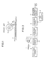
- Fig. 1 shows a general paper thickness detecting apparatus used in a copying machine or a bill identification system as described above.
- a potentiometer 3 is arranged on a path 2 of paper 1.
- This potentiometer 3 includes a rotating shaft 3a and a probe 3b mounted on the rotating shaft 3a, and the distal end of the probe 3b is constantly biased against the paper 1 so as to be in contact with the paper 1.
- the probe 3b is rotated in a direction indicated by an arrow as a paper thickness changes, and a rotational angle of the probe 3b is converted into a voltage change and extracted.
- the potentiometer 3 since a change in thin paper such as a copying sheet or bill is detected by the rotational angle of the probe 3b, a change in rotational angle of the probe 3b with a change in paper thickness obtained when two sheets of paper are fed is very small. In order to correctly detect a change in paper thickness, therefore, the potentiometer 3 must have very high precision. As a result, the arrangement of the apparatus is complicated, and the manufacturing cost of the apparatus is increased.
- the present invention has been made to solve the above conventional problems and has as its object to provide a paper thickness detecting apparatus having a simple arrangement and capable of detecting a change in paper thickness with high precision even if a running speed of paper is increased.
- a paper thickness detecting apparatus comprising an electrode detecting unit constituted by a ground electrode and a detecting electrode arranged to oppose each other in upper and lower positions of a paper path, an oscillating circuit for oscillating an oscillation frequency signal, and a resonant circuit, having a resonator independently of the oscillating circuit, for changing a resonance point in accordance with a change in electrostatic capacitance corresponding to a change in paper thickness detected by the electrode detecting unit.
- a permittivity between the ground electrode and the detecting electrode of the electrode detecting unit changes, a change in paper thickness is detected as a small change in electrostatic capacitance by the electrode detecting unit, and the detection result is supplied to the resonant circuit.
- the resonant circuit shifts a resonance point in correspondence with the change in small electrostatic capacitance detected by the electrode detecting unit and outputs a detection signal corresponding to the change in resonance point. By analyzing this detection signal, a state of two sheets of paper passing through the path is detected as a change in paper thickness.
- a paper thickness detecting apparatus comprising first and second detecting electrodes arranged in front and rear positions of a running path region of paper in a non-contact state with paper, an oscillating circuit for oscillating an oscillation frequency signal, a first resonant circuit, having a resonator independently of the oscillating circuit, for changing a resonance point in response to a change in electrostatic capacitance detected by the first detecting electrode and outputting a detection signal corresponding to the change in resonance point, a second resonant circuit, having a resonator independently of the oscillating circuit and the resonator of the first resonant circuit, for changing a resonance point in response to a change in electrostatic capacitance detected by the second detecting electrode and outputting a detection signal corresponding to the change in resonance point, and an output circuit for outputting a signal indicating a difference between the detection signals from the first and second resonant circuits.
- the first detecting electrode is arranged on the upstream side of the running path region and the second detecting electrode is arranged on the downstream side thereof.
- the paper is detected as a change in electrostatic capacitance in a detection region of the first detecting electrode, and the detection result is supplied to the first resonant circuit.
- the paper reaches the second detecting electrode, the paper is detected as a change in electrostatic capacitance in a detection region of the second detecting electrode, and the detection result is supplied to the second resonant circuit.
- the first and second resonant circuits shift resonance points in response to the changes in electrostatic capacitances supplied from the corresponding detecting electrodes and supply detection signals indicating paper thicknesses corresponding to the changes in resonance points to the output circuit.
- the output circuit obtains a difference between the detection signals supplied from the first and second resonant circuits and supplies the differential signal to a desired signal processing circuit for arithmetically operating a paper thickness or the like.
- a term "paper” is a general term indicating not only a bill and a copying sheet but also a plastic film or sheet.
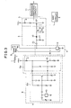
- Fig. 2 is a block diagram showing the first embodiment of a paper thickness detecting apparatus according 'to the present invention
- Fig. 3 is a circuit diagram showing an arrangement of the embodiment in detail.
- the apparatus of this embodiment comprises an oscillating circuit 6 including a high-impedance converting circuit 6a, a resonant circuit 7, an electrode detecting unit 8, a wave detecting circuit 4, an amplifying circuit 5, an AGC circuit (automatic gain control circuit) 9, and an impedance matching circuit 11.
- the head of reference symbol ⁇ indicates a ground point.
- the oscillating circuit 6 is a well known circuit using a ceramic resonator 10 for oscillating an oscillation frequency of a predetermined high frequency fixed within the range of 1 GHz to 10 GHz, e.g., 1 GHz in this embodiment.
- the oscillating circuit 6 supplies a high oscillation frequency signal to the resonant circuit 7 via the high-impedance converting circuit 6a.
- the resonant circuit 7 is constituted by a ceramic resonator 12 which is connected to the electrode detecting unit 8.
- the electrode detecting unit 8 is constituted by a pair of a detecting electrode 14 and a ground electrode 15.
- the detecting and ground electrodes 14 and 15 are located in upper and lower positions of a path 2 of paper 1 to oppose each other via a passing space of the paper 1.
- the detecting electrode 14 is connected to the signal input side of the ceramic resonator 12, and the ground electrode 15 is connected to its ground side.
- the resonant circuit 7 has resonance frequency characteristics, as shown in Fig. 4. Referring to Fig. 4, a fixed oscillation frequency f osc of the oscillating circuit 6 is slightly deviated from a resonance frequency f2 of the resonant circuit 7. The resonance frequency f2 of the resonant circuit 7 is shifted in accordance with a change in electrostatic capacitance between the electrodes 14 and 15 detected by the electrode detecting unit 8, e.g., shifted to f1 when an electrostatic capacitance C changes by + ⁇ C. Since the oscillation frequency of the oscillating circuit 6 is fixed at f osc , the resonant circuit 7 supplies an output voltage V2 at a resonance point A2 if the electrostatic capacitance does not change.
- the resonance frequency is shifted to f1 to change the resonance point from A2 to A1, and the resonant circuit 7 supplies an output voltage V1.
- the resonance frequency of the resonant circuit 7 is shifted in accordance with the change in electrostatic capacitance between the electrodes 14 and 15, and the resonant circuit 7 supplies the output voltage V corresponding to the electrostatic capacitance change accordingly.
- a ceramic dielectric generally has a high (large) Q
- a high detection sensitivity can be expected by constituting the resonator of the circuit by the ceramic resonators 10 and 12.
- the resonant circuit 7 is directly connected to an oscillating circuit unit 6b of the oscillating circuit 6, however, since the impedance of the oscillating circuit unit 6b is lower than that of the ceramic resonator 12 in operation, Q of the resonant circuit 7 is reduced. As a result, since an output voltage at a resonance point is reduced, a satisfactory performance (of high Q) of the resonant circuit 7 cannot be obtained.
- the high-impedance converting circuit 6a is provided between the oscillating circuit unit 6b and the resonant circuit 7.
- the high-impedance converting circuit 6a is constituted as a high-impedance circuit by connecting circuit elements such as a transistor 13, a resistor, and a capacitor.
- the transistor 13 applies a high impedance to the resonant circuit 7 by an emitter-follower connection and intercepts a mutual interference between the oscillating circuit unit 6b on the ceramic resonator 10 side and the resonant circuit 7 on the ceramic resonator 12 side.
- the wave detecting circuit 4 is connected to the resonant circuit 7 via a coupling capacitor 25.
- This wave detecting circuit 4 is constituted by an inductance element 21, a diode 22, a capacitor 23, and a resistor 24 and receives an output signal from the resonant circuit 7 via the coupling capacitor 25.
- the diode 22, the capacitor 23, and the resistor 24 constitute a signal detecting circuit, and the inductance element 21 and the capacitor 25 serve as a high-impedance circuit.
- the wave detecting circuit 4 envelope-detects an output signal from the resonant circuit 7 having a high frequency and converts the signal into a signal for detecting a paper thickness.
- the amplifying circuit 5 is constituted by a transistor 27 and an element such as a resistor.
- the amplifying circuit 5 amplifies a signal supplied from the wave detecting circuit 4 and supplies the signal to a signal processing circuit (not shown) via the impedance matching circuit 11 and to the AGC circuit 9.
- the AGC circuit 9 prevents the gain of the transistor 27 from falling outside the set gain range for paper thickness detection due to disturbance such as rumples or a rupture of the paper 1, thereby enabling correct detection of a paper thickness even if the paper 1 has a rupture or rumples.
- the oscillation frequency f osc of the oscillating circuit 6 is slightly deviated from the resonance frequency f2 of the resonant circuit 7, as shown in Fig. 4.
- the resonant circuit 7 outputs a constant voltage V2.
- the resonance frequency of the resonant circuit 7 is shifted from f2 to f1 with respect to the oscillation frequency f osc of the oscillating circuit 6, the resonance point changes from A2 to A1, and the resonant circuit 7 outputs a voltage V1.
- the permittivity between the electrodes 14 and 15 further changes, the resonance frequency of the resonant circuit 7 is shifted to f0, the resonance point changes from A1 to A0, and the resonant circuit 7 outputs a voltage V0.
- the resonant circuit 7 forms an amplitude modulation wave in accordance with the change in output voltage corresponding to the paper thicknesses and supplies the modulation wave to the wave detecting circuit 4. That is, the resonant circuit 7 performs multiplication between the oscillation frequency f osc and a change component ⁇ f of the resonance frequency corresponding to the change in paper thickness and obtains the amplitude modulation (AM) wave.
- the oscillation frequency f osc is 1 GHz
- a detection signal as a modulation wave is obtained as a signal having a high frequency corresponding to the change in paper thickness and having a frequency of 1 GHz as the center, and this signal having a high frequency is supplied to the wave detecting circuit 4.
- the wave detecting circuit performs envelope detection to convert this high-frequency signal into a signal for paper thickness detection (in this embodiment, a signal of 3 MHz).
- This band-converted signal is amplified by an amplifying circuit of the transistor 27.
- An output signal from the transistor 27 is supplied to the signal processing circuit (not shown) via the impedance matching circuit 11, and is also supplied to the AGC circuit 9.
- the AGC circuit 9 corrects deviation of the gain of the transistor 27 from the set gain range for paper thickness detection due to disturbance such as rumples or a rupture of the paper 1 and adjusts it in an optimal position in a linear region of the resonance frequency curve in Fig. 4.
- the thickness of the paper 1 passing through the path 2 is detected in a non-contact state. Even if the running speed of the paper 1 is increased, therefore, the apparatus can reliably follow the paper 1 to correctly detect a change in paper thickness or overlapping of sheets of paper.
- the resonators of the oscillating circuit 6 and the resonant circuit 7 are constituted by the ceramic resonators 10 and 12, a large Q value with respect to the resonant circuit 7 can be obtained.
- peripheral circuits of the resonant circuit 7, i.e., the impedance converting circuit 6a and a resonating circuit of the inductance element 21 and the capacitor 25 are constituted by high-impedance circuits, a small change in electrostatic capacitance can be detected with high sensitivity during an operation of the resonant circuit 7 without producing Q damp.
- the apparatus can have a very small size.
- the present invention is not limited to the above embodiment but can be variously modified.
- the resonators of the oscillating circuit 6 and the resonant circuit 7 are made of materials having the same temperature characteristics, a paper thickness detecting apparatus having high temperature stability can be obtained.
- Fig. 5 is a block diagram showing the second embodiment of a paper thickness detecting apparatus according to the present invention.
- the apparatus of the second embodiment comprises an oscillating circuit 6, a distributor 16, a first sensor circuit 11a, a second sensor circuit 11b, a differential amplifier 17 as an output circuit, a first electrode detecting unit 8a, and a second electrode detecting unit 8b.
- the first electrode detecting unit 8a is constituted by a detecting electrode 14a and a ground electrode
- the second electrode detecting unit 8b is constituted by a detecting electrode 14b and the ground electrode 15.
- the ground electrode 15 and the detecting electrodes 14a and 14b are arranged to sandwich a running path region 2 of paper 1, i.e., arranged to oppose each other via a passing space of the paper 1.
- the detecting electrode 14a is arranged on the upstream side of the detecting electrode 14b.
- the first and second sensor circuits 11a and 11b have the same circuit arrangement.
- Fig. 6 is a circuit diagram showing in detail the oscillating circuit 6, the distributor 16, the first sensor circuit 11a, and the first electrode detecting unit 8a.
- the oscillating circuit 6 is the same as the oscillating circuit in the first embodiment of the present invention.
- This oscillating circuit 6 oscillates an oscillation frequency signal having a high frequency and supplies the signal to the distributor 16 via a high impedance converting circuit 6a.
- the distributor 16 distributes this oscillation frequency signal to the first and second sensor circuits 11a and 11b.
- the sensor circuit 11a is constituted by a resonant circuit (first resonant circuit) 7a, a wave detecting circuit 4a, an AFC circuit (automatic frequency control circuit) 9a, and an amplifying circuit 5a.
- the resonant circuit 7a is constituted by a ceramic resonator 12, and the detecting electrode 14a of the electrode detecting unit 8a is connected to the signal input side of the resonant circuit 7a.
- the ground electrode 15 is connected to the ground side of the resonant circuit 7a.
- a fixed oscillation frequency f osc of the oscillating circuit 6 is slightly deviated from a resonance frequency f2 of the resonant circuit 7a as similarly shown in Fig. 4.
- the resonance frequency f2 of the resonant circuit 7a is shifted in accordance with a change in electrostatic capacitance between the electrodes 14a and 15 detected by the electrode detecting unit 8a, e.g., shifted to f1 when an electrostatic capacitance C changes by + ⁇ C. Since the oscillation frequency of the oscillating circuit 6 is fixed at f ocs , the resonant circuit 7a supplies an output voltage V2 at a resonance point A2 when the electrostatic capacitance does not change.
- the resonance frequency of the resonant circuit 7a is shifted in accordance with the change in electrostatic capacitance between the electrodes 14a and 15, and the resonant circuit 7a supplies the output voltage V corresponding to the electrostatic capacitance change.
- the wave detecting circuit 4a receives an output signal from the resonant circuit 7a via a coupling capacitor 25.
- the wave detecting circuit 4a envelope-detects the output signal output from the resonant circuit 7a and having a high frequency, converts the signal into a signal having a signal band for detecting a paper thickness, and supplies the converted signal to the amplifying circuit 5a and the AFC circuit 9a.
- the amplifying circuit 5a amplifies the signal from the wave detecting circuit 4a and supplies the amplified signal to the differential amplifier.
- the AFC circuit 9a prevents the resonance point from falling outside the set frequency range for paper thickness detection due to disturbance such as rumples or a rupture of the paper 1, thereby enabling correct detection of a paper thickness even if the paper 1 has a rupture or rumples.
- this embodiment includes the second sensor circuit 11b having the same arrangement as that of the first sensor circuit 11a.
- the second sensor circuit 11b also receives the oscillation frequency signal supplied from the oscillating circuit 6 and distributed by the distributor 16 and performs the same circuit operation as that of the first sensor circuit.
- the fixed oscillation frequency f osc of the oscillating circuit 6 is slightly deviated from the resonance frequency f2 of the resonant circuits 7a and 7b, as shown in Fig. 4.
- the resonant circuits 7a and 7b output a constant voltage V2.
- the resonance frequency of the resonant circuit 7a on the first sensor circuit 11a is shifted from f2 to f1, the resonance point changes from A2 to A1, and the resonant circuit 7a outputs a voltage V1.
- the resonance frequency of the resonant circuit 7a is shifted to f0, the resonance point changes from A1 to A0, and the resonant circuit 7a outputs a voltage V0.
- the second electrode detecting unit 8b when the paper 1 passes between the detecting electrode 14b and the ground electrode 15, a change in electrostatic capacitance corresponding to the passing of the paper 1 is detected by the second electrode detecting unit 8b, the detection result is supplied to the resonant circuit 7b on the second sensor circuit 11b, and the circuit 7b outputs an output voltage corresponding to a paper thickness.
- the first and second resonant circuits form an AM wave from the changes in output voltages corresponding to the paper thickness and supply the formed waves as detection signals to the corresponding wave detecting circuits 4a and 4b.
- the first resonant circuit 7a performs multiplication between the oscillation frequency f osc and a change component ⁇ f of the resonance frequency corresponding to the change in paper thickness detected by the detecting electrode 14a and obtains the AM wave.
- the second resonant circuit 7b performs multiplication between the oscillation frequency f osc and a change component ⁇ f of the resonance frequency corresponding to the change in paper thickness detected by the detecting electrode 14b and obtains the AM wave.
- the oscillation frequency f osc is 1GHz
- a detection signal as an AM wave is a signal of a high frequency corresponding to the change in paper thickness and having 1 GHz as the ceter. This high-frequency signal is supplied from each resonant circuit to a corresponding one of the wave detecting circuits 4a and 4b.
- the wave detecting circuit 4a (4b) envelope-detects this high-frequency signal to convert the signal into a signal for detecting a paper thickness (in this embodiment, a signal having a frequency of 3 MHz).
- This band-converted signal is amplified by the amplifying circuit 5a (5b) and supplied to the differential amplifier 17.
- the band-converted signal is also supplied to the AFC circuit 9a (9b).
- the AFC circuit 9a (9b) corrects deviation of the resonance point from the set gain range for paper thickness detection due to disturbance such as rumples or a rupture of the paper 1 and adjusts it in an optimal position in a linear region of a resonance frequency curve having a high variation.
- the differential amplifier 17 obtains a difference between the signals supplied from the amplifying circuits 5a and 5b and supplies the obtained differential output to a desired signal processing circuit (not shown).
- Figs. 7A and 7B show waveforms of the differential output obtained by the differential amplifier 17. For example, when one sheet of the paper 1 runs through the running path region 2 and a leading end A of the paper 1 comes to a position immediately below the detecting electrode 14a, as indicated by a solid line in Fig. 5, a change in electrostatic capacitance between the detecting and ground electrodes 14a and 15 is detected not by the electrode detecting unit 8b but by the electrode detecting unit 8a. Therefore, as shown in Fig. 7A, the-differential output between the first and second signals of the sensor circuits 11a and 11b appears as a peak S1 projecting in the negative direction.
- an electrostatic capacitance C between the detecting electrodes 14a and 14b and the ground electrode 15 is determined by a space permittivity E, a permittivity E1 of paper, a thickness nl ( n is an integer) of the paper, and a space width L - nl.
- the differential amplifier 17 outputs a pulse signal S A in the negative direction when a leading end A of the paper passes through the detecting electrode 14a, and the differential output becomes zero when the leading end A of the paper A reaches the detecting electrode 14b.
- a pulse waveform S B appears when a leading end B of the overlapping paper passes through the detecting electrode 14a, and the differential output becomes zero when the leading end B of the paper reaches the detecting electrode 14b.
- a pulse waveform S C appears to-project upward.
- the differential output becomes zero.
- a pulse waveform S D appears in the same polarity as that of S C .
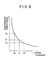
- the height of a pulse waveform is determined by the number of sheets of paper. That is, as shown in Fig. 9, the electrostatic capacitance is in inverse proportion to the thickness of paper. More specifically, while the electrostatic capacitance is C0 when no paper is present (l0 in Fig.
- the length of the paper 1 can be obtained by an interval between the pulse waveforms S A and S C .
- the deviation between two sheets of paper can be obtained on the basis of the interval between the pulse waveforms S A and S B .
- the detecting electrodes 14a and 14b are arranged close to each other and their electrode areas are minimized, a small deviation between two sheets of paper can be obtained with high precision.
- the thickness of the paper 1 passing through the running path region 2 is detected in a non-contact state. Even if the running speed of the paper 1 is increased, therefore, the apparatus can reliably follow the movement of the paper to correctly detect a change in paper thickness or overlapping of sheets of paper.
- a paper thickness of interest can be detected with high precision.
- detection of a paper thickness or the like is performed on the basis of a signal indicating a difference between the detection signals on the first and second sensor circuits 11a and 11b, disturbance components of an environmental change such as a temperature or a humidity can be canceled to be removed. As a result, detection of a paper thickness or the like can be performed with high reliability.
- the resonator of the oscillating circuit 6 and the resonators of the resonant circuits 7a and 7b are constituted by the ceramic resonators 10 and 12, a large Q value of the circuits 6b and 7 can be obtained.
- peripheral circuits of the resonant circuit 7, i.e., the impedance converting circuit 6a and the resonating circuit of the inductance element 21 and the capacitor 25 are constituted by high-impedance circuits, a small change in electrostatic capacitance can be detected with high precision without producing Q damp during an operation of the resonant circuit.
- the apparatus can have a very small size.
- a pair of the front and rear electrode detecting units are arranged along the running path region of paper in a non-contact state with paper, and a paper thickness or the like is detected by using a change in electrostatic capacitance of electrode detection regions obtained when paper passes through the electrode detecting units in a non-contact state. Even if the running speed of the paper is increased, therefore, the apparatus can reliably follow the movement of the paper to correctly detect its thickness.
- the resonance point of the resonant circuit is shifted by using a change in electrostatic capacitance corresponding to a change in paper thickness, thereby obtaining the paper thickness.
- a small change in paper thickness can be correctly detected, and the manufacturing cost of the apparatus can be reduced.
- the paper thickness is detected on the basis of a differential output between signals obtained by the first and second sensor circuits, disturbance components can be canceled to be removed. Therefore, information indicating, e.g. a paper thickness, overlapping of sheets of paper, a paper length, or a deviation between overlapped sheets of paper can be detected with high sensitivity, high precision, and high reliability, resulting in a very large technical value.
Landscapes
- Physics & Mathematics (AREA)
- General Physics & Mathematics (AREA)
- Measurement Of Length, Angles, Or The Like Using Electric Or Magnetic Means (AREA)
Applications Claiming Priority (4)
| Application Number | Priority Date | Filing Date | Title |
|---|---|---|---|
| JP13276/90 | 1990-02-14 | ||
| JP1990013276U JPH0744965Y2 (ja) | 1990-02-14 | 1990-02-14 | 紙厚検出装置 |
| JP2035571A JPH0752083B2 (ja) | 1990-02-16 | 1990-02-16 | 紙厚検出装置 |
| JP35571/90 | 1990-02-16 |
Publications (3)
| Publication Number | Publication Date |
|---|---|
| EP0442727A2 true EP0442727A2 (fr) | 1991-08-21 |
| EP0442727A3 EP0442727A3 (en) | 1992-03-18 |
| EP0442727B1 EP0442727B1 (fr) | 1996-10-30 |
Family
ID=26349044
Family Applications (1)
| Application Number | Title | Priority Date | Filing Date |
|---|---|---|---|
| EP91301173A Expired - Lifetime EP0442727B1 (fr) | 1990-02-14 | 1991-02-13 | Appareil pour détecter l'épaisseur de papier |
Country Status (3)
| Country | Link |
|---|---|
| US (1) | US5198777A (fr) |
| EP (1) | EP0442727B1 (fr) |
| DE (1) | DE69122895T2 (fr) |
Cited By (5)
| Publication number | Priority date | Publication date | Assignee | Title |
|---|---|---|---|---|
| EP0509731A3 (en) * | 1991-04-15 | 1993-06-09 | Murata Manufacturing Co., Ltd. | Electrostatic sensor apparatus |
| EP0586349A1 (fr) * | 1992-06-17 | 1994-03-09 | G.D Societa' Per Azioni | Appareil de mesure de l'épaisseur d'un matériau en bande, en particulier dans un dispositif de changement automatique de bobines de matériau métallisé en bande |
| WO2007137761A1 (fr) * | 2006-06-01 | 2007-12-06 | Dahle Bürotechnik Gmbh | Destructeur de documents |
| EP2180290A1 (fr) * | 2007-08-02 | 2010-04-28 | Acco UK Limited | Déchiqueteuse |
| CN113280725A (zh) * | 2021-03-09 | 2021-08-20 | 歌尔微电子股份有限公司 | 石英晶体厚度检测装置 |
Families Citing this family (48)
| Publication number | Priority date | Publication date | Assignee | Title |
|---|---|---|---|---|
| US5412318A (en) * | 1992-03-17 | 1995-05-02 | Landis & Gyr Business Support Ag | Device for detecting attempts at fraud on an apparatus for reading and writing on a chip card |
| ZA934445B (en) * | 1992-06-22 | 1994-01-24 | David John Radford | Radio frequency measuring apparatus |
| FR2692978A1 (fr) * | 1992-06-30 | 1993-12-31 | Alcatel Fibres Optiques | Dispositif et procédé de contrôle de l'épaisseur et de la régularité d'un revêtement déposé sur un corps isolant allongé. |
| US5321366A (en) * | 1992-08-31 | 1994-06-14 | Murata Mfg. Co. Ltd. | Capacitance sensor apparatus of divided multi-electrode type |
| JP2922376B2 (ja) * | 1992-12-26 | 1999-07-19 | キヤノン株式会社 | シート厚測定装置 |
| US5455565A (en) * | 1993-11-08 | 1995-10-03 | Ivac Corporation | Fluid monitor system and method using a resonator |
| US5808435A (en) * | 1996-05-28 | 1998-09-15 | Kmy Instruments | Micropositioning device for disk head testing system |
| US5922959A (en) * | 1996-10-15 | 1999-07-13 | Currency Systems International | Methods of measuring currency limpness |
| US6341522B1 (en) | 1996-12-13 | 2002-01-29 | Measurex Corporation | Water weight sensor array imbedded in a sheetmaking machine roll |
| US5928475A (en) * | 1996-12-13 | 1999-07-27 | Honeywell-Measurex, Corporation | High resolution system and method for measurement of traveling web |
| US6072309A (en) * | 1996-12-13 | 2000-06-06 | Honeywell-Measurex Corporation, Inc. | Paper stock zeta potential measurement and control |
| US6087837A (en) | 1996-12-13 | 2000-07-11 | Honeywell-Measurex | Compact high resolution under wire water weight sensor array |
| US5891306A (en) * | 1996-12-13 | 1999-04-06 | Measurex Corporation | Electromagnetic field perturbation sensor and methods for measuring water content in sheetmaking systems |
| US5853543A (en) * | 1997-01-27 | 1998-12-29 | Honeywell-Measurex Corporation | Method for monitoring and controlling water content in paper stock in a paper making machine |
| US6168080B1 (en) | 1997-04-17 | 2001-01-02 | Translucent Technologies, Llc | Capacitive method and apparatus for accessing contents of envelopes and other similarly concealed information |
| US5944955A (en) * | 1998-01-15 | 1999-08-31 | Honeywell-Measurex Corporation | Fast basis weight control for papermaking machine |
| US6092003A (en) * | 1998-01-26 | 2000-07-18 | Honeywell-Measurex Corporation | Paper stock shear and formation control |
| US6076022A (en) * | 1998-01-26 | 2000-06-13 | Honeywell-Measurex Corporation | Paper stock shear and formation control |
| US6080278A (en) * | 1998-01-27 | 2000-06-27 | Honeywell-Measurex Corporation | Fast CD and MD control in a sheetmaking machine |
| US6149770A (en) * | 1998-04-14 | 2000-11-21 | Honeywell-Measurex Corporation | Underwire water weight turbulence sensor |
| US6168687B1 (en) | 1998-04-24 | 2001-01-02 | Honeywell-Measurex Corporation | System and method for sheet measurement and control in papermaking machine |
| US6006602A (en) * | 1998-04-30 | 1999-12-28 | Honeywell-Measurex Corporation | Weight measurement and measurement standardization sensor |
| US6086716A (en) * | 1998-05-11 | 2000-07-11 | Honeywell-Measurex Corporation | Wet end control for papermaking machine |
| DE19826909A1 (de) * | 1998-06-17 | 1999-12-23 | Koenig & Bauer Ag | Einrichtung zur kapazitiven Doppelbogenkontrolle |
| US6202929B1 (en) | 1999-03-10 | 2001-03-20 | Micro-Epsilon Mess Technik | Capacitive method and apparatus for accessing information encoded by a differentially conductive pattern |
| US6995574B2 (en) | 2003-12-18 | 2006-02-07 | The Boeing Company | Measurement of a coating on a composite using capacitance |
| US7954737B2 (en) | 2007-10-04 | 2011-06-07 | Fellowes, Inc. | Shredder thickness with anti-jitter feature |
| US8870106B2 (en) * | 2004-09-10 | 2014-10-28 | Fellowes, Inc. | Shredder with thickness detector |
| US7631822B2 (en) * | 2004-09-10 | 2009-12-15 | Fellowes Inc. | Shredder with thickness detector |
| US8672247B2 (en) | 2005-07-11 | 2014-03-18 | Fellowes, Inc. | Shredder with thickness detector |
| DE102006038339B4 (de) * | 2006-08-15 | 2008-08-21 | Andritz Küsters GmbH & Co. KG | Verfahren und Vorrichtung zur Ausrüstung einer Warenbahn |
| US8922226B2 (en) * | 2006-08-28 | 2014-12-30 | Detection Systems Pty Ltd | Production line detection apparatus and method |
| EP2174899B1 (fr) * | 2007-07-26 | 2017-12-27 | Fujitsu Limited | Dispositif de détection d'épaisseur de feuille de papier |
| US8430347B2 (en) * | 2009-01-05 | 2013-04-30 | Fellowes, Inc. | Thickness adjusted motor controller |
| US8201761B2 (en) * | 2009-01-05 | 2012-06-19 | Fellowes, Inc. | Thickness sensor based motor controller |
| US8091809B2 (en) * | 2009-03-24 | 2012-01-10 | Fellowes, Inc. | Shredder with jam proof system |
| US8205815B2 (en) * | 2009-05-15 | 2012-06-26 | Fellowes, Inc. | Paper alignment sensor arrangement |
| US8550387B2 (en) * | 2009-06-18 | 2013-10-08 | Tai Hoon K. Matlin | Restrictive throat mechanism for paper shredders |
| US8678305B2 (en) * | 2009-06-18 | 2014-03-25 | Fellowes, Inc. | Restrictive throat mechanism for paper shredders |
| US8382019B2 (en) | 2010-05-03 | 2013-02-26 | Fellowes, Inc. | In-rush current jam proof sensor control |
| US8511593B2 (en) | 2010-05-28 | 2013-08-20 | Fellowes, Inc. | Differential jam proof sensor for a shredder |
| GB2481002B (en) * | 2010-06-04 | 2015-01-14 | Plastic Logic Ltd | Determining layer thickness |
| GB201011785D0 (en) * | 2010-07-13 | 2010-08-25 | Oxford Rf Sensors Ltd | Permittivity sensor |
| US8854056B1 (en) * | 2012-09-13 | 2014-10-07 | Cypress Semiconductor Corporation | Capacitance sensing devices and methods |
| US9746385B2 (en) * | 2013-06-12 | 2017-08-29 | Honeywell International Inc. | System and method for measuring varying parameters using adaptive signal conditioning |
| WO2016170639A1 (fr) * | 2015-04-23 | 2016-10-27 | 富士通フロンテック株式会社 | Capteur de détection de l'épaisseur de feuilles de papier et unité de distinction de billets de banque |
| US10209054B2 (en) * | 2016-04-20 | 2019-02-19 | Duke University | Non-invasive thickness measurement using capacitance measurement |
| CN109297397B (zh) * | 2018-10-25 | 2020-07-31 | 中国电子产品可靠性与环境试验研究所((工业和信息化部电子第五研究所)(中国赛宝实验室)) | 静电换能器可动电极的厚度测量方法、装置以及系统 |
Family Cites Families (11)
| Publication number | Priority date | Publication date | Assignee | Title |
|---|---|---|---|---|
| US2562575A (en) * | 1947-01-04 | 1951-07-31 | Emhart Mfg Co | Electronic device for measuring physical constants |
| FR1297916A (fr) * | 1961-05-26 | 1962-07-06 | Commissariat Energie Atomique | Dispositif pour la mesure de l'épaisseur d'un film liquide |
| US3300716A (en) * | 1962-04-21 | 1967-01-24 | Cons Electrodynamics Corp | Apparatus for measuring and testing electrical properties of nonconductive materials |
| US3341774A (en) * | 1962-07-17 | 1967-09-12 | Comm Res Inc | Capacitance detector having a transmitter connected to one plate and a receiver connected to another plate |
| US3519922A (en) * | 1965-12-16 | 1970-07-07 | Nash & Harrison Ltd | Apparatus for detecting abrupt change in the thickness of sheet material |
| US3609735A (en) * | 1968-12-03 | 1971-09-28 | Harris Intertype Corp | Inductive-capacitive probe in machine for handling sheetlike material |
| US3990005A (en) * | 1974-09-03 | 1976-11-02 | Ade Corporation | Capacitive thickness gauging for ungrounded elements |
| US4528655A (en) * | 1981-11-16 | 1985-07-09 | Murata Manufacturing Co., Ltd. | Apparatus for detecting variation of electrostatic capacitance |
| FR2528970B1 (fr) * | 1982-06-22 | 1985-09-27 | Flonic Sa | Dispositif de verification d'epaisseur de matieres dielectriques en feuille |
| GB8709465D0 (en) * | 1987-04-22 | 1987-05-28 | Watkiss Automation Ltd | Sensor |
| JPH06101052B2 (ja) * | 1988-06-30 | 1994-12-12 | 株式会社日本コンラックス | 硬貨識別装置 |
-
1991
- 1991-02-12 US US07/654,425 patent/US5198777A/en not_active Expired - Lifetime
- 1991-02-13 EP EP91301173A patent/EP0442727B1/fr not_active Expired - Lifetime
- 1991-02-13 DE DE69122895T patent/DE69122895T2/de not_active Expired - Fee Related
Cited By (10)
| Publication number | Priority date | Publication date | Assignee | Title |
|---|---|---|---|---|
| EP0509731A3 (en) * | 1991-04-15 | 1993-06-09 | Murata Manufacturing Co., Ltd. | Electrostatic sensor apparatus |
| US5325067A (en) * | 1991-04-15 | 1994-06-28 | Murata Mfg. Co., Ltd. | Apparatus for matching impedance in an electrostatic sensor |
| EP0586349A1 (fr) * | 1992-06-17 | 1994-03-09 | G.D Societa' Per Azioni | Appareil de mesure de l'épaisseur d'un matériau en bande, en particulier dans un dispositif de changement automatique de bobines de matériau métallisé en bande |
| US5521498A (en) * | 1992-06-17 | 1996-05-28 | G.D S.P.A. | Device for sensing the thickness of strip material in particular in devices for changing rolls of metallized strip material automatically |
| WO2007137761A1 (fr) * | 2006-06-01 | 2007-12-06 | Dahle Bürotechnik Gmbh | Destructeur de documents |
| EP2180290A1 (fr) * | 2007-08-02 | 2010-04-28 | Acco UK Limited | Déchiqueteuse |
| US9669410B2 (en) | 2007-08-02 | 2017-06-06 | ACCO Brands Corporation | Shredding machine |
| US10576476B2 (en) | 2007-08-02 | 2020-03-03 | ACCO Brands Corporation | Shredding machine |
| CN113280725A (zh) * | 2021-03-09 | 2021-08-20 | 歌尔微电子股份有限公司 | 石英晶体厚度检测装置 |
| CN113280725B (zh) * | 2021-03-09 | 2022-10-28 | 歌尔微电子股份有限公司 | 石英晶体厚度检测装置 |
Also Published As
| Publication number | Publication date |
|---|---|
| DE69122895D1 (de) | 1996-12-05 |
| US5198777A (en) | 1993-03-30 |
| EP0442727A3 (en) | 1992-03-18 |
| DE69122895T2 (de) | 1997-05-28 |
| EP0442727B1 (fr) | 1996-10-30 |
Similar Documents
| Publication | Publication Date | Title |
|---|---|---|
| US5198777A (en) | Paper thickness detecting apparatus having a resonator with a resonance point set by a capacitance detecting unit | |
| US5231359A (en) | Ceramic resonance type electrostatic sensor apparatus | |
| US5587529A (en) | Angular rate detector | |
| AU671316B2 (en) | Oscillator circuit | |
| US4868488A (en) | Use of a dielectric microwave resonator and sensor circuit for determining the position of a body | |
| US10269200B2 (en) | Paper sheet thickness detecting sensor and banknote classifying unit | |
| JPH0752083B2 (ja) | 紙厚検出装置 | |
| JPH0816942B2 (ja) | スレッド内蔵紙葉の検査装置 | |
| JP2518170B2 (ja) | 静電センサ装置 | |
| JPH0744965Y2 (ja) | 紙厚検出装置 | |
| JPH0599605A (ja) | 非接触式厚み検出装置 | |
| JPH0711545B2 (ja) | 多チャンネル静電センサ装置 | |
| JP3327706B2 (ja) | 紙葉検査用静電容量センサの検出点最適化方法 | |
| JP2652575B2 (ja) | 移動体の静電検出装置 | |
| JP2518187B2 (ja) | 静電センサ装置 | |
| JPH03123873A (ja) | 多連静電センサ装置 | |
| JP3116693B2 (ja) | 静電センサ | |
| JPH0820478B2 (ja) | 静電センサ装置 | |
| JP3307032B2 (ja) | 静電センサ | |
| JPH04186168A (ja) | 静電センサ装置 | |
| JP2531003B2 (ja) | セラミック共振形静電センサ装置 | |
| JPH0769371B2 (ja) | セラミック形静電センサの可変出力回路 | |
| JP2530866Y2 (ja) | セラミック共振器形静電センサの検波増幅回路 | |
| JP2508685Y2 (ja) | 静電センサ装置 | |
| JPS63316515A (ja) | 近接センサ |
Legal Events
| Date | Code | Title | Description |
|---|---|---|---|
| PUAI | Public reference made under article 153(3) epc to a published international application that has entered the european phase |
Free format text: ORIGINAL CODE: 0009012 |
|
| AK | Designated contracting states |
Kind code of ref document: A2 Designated state(s): DE GB IT |
|
| PUAL | Search report despatched |
Free format text: ORIGINAL CODE: 0009013 |
|
| AK | Designated contracting states |
Kind code of ref document: A3 Designated state(s): DE GB IT |
|
| 17P | Request for examination filed |
Effective date: 19920604 |
|
| 17Q | First examination report despatched |
Effective date: 19931028 |
|
| GRAG | Despatch of communication of intention to grant |
Free format text: ORIGINAL CODE: EPIDOS AGRA |
|
| GRAH | Despatch of communication of intention to grant a patent |
Free format text: ORIGINAL CODE: EPIDOS IGRA |
|
| GRAH | Despatch of communication of intention to grant a patent |
Free format text: ORIGINAL CODE: EPIDOS IGRA |
|
| GRAA | (expected) grant |
Free format text: ORIGINAL CODE: 0009210 |
|
| AK | Designated contracting states |
Kind code of ref document: B1 Designated state(s): DE GB IT |
|
| ITF | It: translation for a ep patent filed | ||
| REF | Corresponds to: |
Ref document number: 69122895 Country of ref document: DE Date of ref document: 19961205 |
|
| PLBE | No opposition filed within time limit |
Free format text: ORIGINAL CODE: 0009261 |
|
| STAA | Information on the status of an ep patent application or granted ep patent |
Free format text: STATUS: NO OPPOSITION FILED WITHIN TIME LIMIT |
|
| 26N | No opposition filed | ||
| REG | Reference to a national code |
Ref country code: GB Ref legal event code: IF02 |
|
| PGFP | Annual fee paid to national office [announced via postgrant information from national office to epo] |
Ref country code: GB Payment date: 20060208 Year of fee payment: 16 |
|
| PGFP | Annual fee paid to national office [announced via postgrant information from national office to epo] |
Ref country code: DE Payment date: 20060209 Year of fee payment: 16 |
|
| PGFP | Annual fee paid to national office [announced via postgrant information from national office to epo] |
Ref country code: IT Payment date: 20060228 Year of fee payment: 16 |
|
| GBPC | Gb: european patent ceased through non-payment of renewal fee |
Effective date: 20070213 |
|
| PG25 | Lapsed in a contracting state [announced via postgrant information from national office to epo] |
Ref country code: DE Free format text: LAPSE BECAUSE OF NON-PAYMENT OF DUE FEES Effective date: 20070901 |
|
| PG25 | Lapsed in a contracting state [announced via postgrant information from national office to epo] |
Ref country code: GB Free format text: LAPSE BECAUSE OF NON-PAYMENT OF DUE FEES Effective date: 20070213 |
|
| PG25 | Lapsed in a contracting state [announced via postgrant information from national office to epo] |
Ref country code: IT Free format text: LAPSE BECAUSE OF NON-PAYMENT OF DUE FEES Effective date: 20070213 |