EP0443277A1 - Corps céramique métallisé et méthode pour le produire - Google Patents
Corps céramique métallisé et méthode pour le produire Download PDFInfo
- Publication number
- EP0443277A1 EP0443277A1 EP90400458A EP90400458A EP0443277A1 EP 0443277 A1 EP0443277 A1 EP 0443277A1 EP 90400458 A EP90400458 A EP 90400458A EP 90400458 A EP90400458 A EP 90400458A EP 0443277 A1 EP0443277 A1 EP 0443277A1
- Authority
- EP
- European Patent Office
- Prior art keywords
- gas
- ceramic body
- sintered ceramic
- tungsten
- process according
- Prior art date
- Legal status (The legal status is an assumption and is not a legal conclusion. Google has not performed a legal analysis and makes no representation as to the accuracy of the status listed.)
- Granted
Links
- 239000000919 ceramic Substances 0.000 title claims abstract description 44
- 238000000034 method Methods 0.000 title claims abstract description 41
- BLRPTPMANUNPDV-UHFFFAOYSA-N Silane Chemical class [SiH4] BLRPTPMANUNPDV-UHFFFAOYSA-N 0.000 claims abstract description 35
- 229910052721 tungsten Inorganic materials 0.000 claims abstract description 19
- 229910052750 molybdenum Inorganic materials 0.000 claims abstract description 18
- 239000010937 tungsten Substances 0.000 claims abstract description 17
- 239000011733 molybdenum Substances 0.000 claims abstract description 16
- WFKWXMTUELFFGS-UHFFFAOYSA-N tungsten Chemical compound [W] WFKWXMTUELFFGS-UHFFFAOYSA-N 0.000 claims abstract description 14
- 229910052751 metal Inorganic materials 0.000 claims abstract description 11
- 239000002184 metal Substances 0.000 claims abstract description 11
- 229910001092 metal group alloy Inorganic materials 0.000 claims abstract description 5
- -1 molybdenum halide Chemical class 0.000 claims abstract 8
- 239000007789 gas Substances 0.000 claims description 44
- 238000000151 deposition Methods 0.000 claims description 21
- 230000008021 deposition Effects 0.000 claims description 18
- 229910017083 AlN Inorganic materials 0.000 claims description 16
- PIGFYZPCRLYGLF-UHFFFAOYSA-N Aluminum nitride Chemical compound [Al]#N PIGFYZPCRLYGLF-UHFFFAOYSA-N 0.000 claims description 16
- ZOKXTWBITQBERF-UHFFFAOYSA-N Molybdenum Chemical compound [Mo] ZOKXTWBITQBERF-UHFFFAOYSA-N 0.000 claims description 10
- 239000003870 refractory metal Substances 0.000 claims description 10
- 229910052990 silicon hydride Inorganic materials 0.000 claims description 10
- 229910001507 metal halide Inorganic materials 0.000 claims description 9
- 150000005309 metal halides Chemical class 0.000 claims description 9
- PNEYBMLMFCGWSK-UHFFFAOYSA-N Alumina Chemical compound [O-2].[O-2].[O-2].[Al+3].[Al+3] PNEYBMLMFCGWSK-UHFFFAOYSA-N 0.000 claims description 8
- XUIMIQQOPSSXEZ-UHFFFAOYSA-N Silicon Chemical compound [Si] XUIMIQQOPSSXEZ-UHFFFAOYSA-N 0.000 claims description 8
- 229910015255 MoF6 Inorganic materials 0.000 claims description 7
- 239000000463 material Substances 0.000 claims description 7
- 239000000203 mixture Substances 0.000 claims description 7
- RLCOZMCCEKDUPY-UHFFFAOYSA-H molybdenum hexafluoride Chemical compound F[Mo](F)(F)(F)(F)F RLCOZMCCEKDUPY-UHFFFAOYSA-H 0.000 claims description 7
- 229910010293 ceramic material Inorganic materials 0.000 claims description 6
- 229910052575 non-oxide ceramic Inorganic materials 0.000 claims description 5
- 229910052574 oxide ceramic Inorganic materials 0.000 claims description 5
- VEXZGXHMUGYJMC-UHFFFAOYSA-M Chloride anion Chemical compound [Cl-] VEXZGXHMUGYJMC-UHFFFAOYSA-M 0.000 claims description 2
- KRHYYFGTRYWZRS-UHFFFAOYSA-M Fluoride anion Chemical compound [F-] KRHYYFGTRYWZRS-UHFFFAOYSA-M 0.000 claims description 2
- 238000004519 manufacturing process Methods 0.000 claims description 2
- HBMJWWWQQXIZIP-UHFFFAOYSA-N silicon carbide Chemical compound [Si+]#[C-] HBMJWWWQQXIZIP-UHFFFAOYSA-N 0.000 claims description 2
- 229910010271 silicon carbide Inorganic materials 0.000 claims description 2
- 229910000077 silane Inorganic materials 0.000 claims 5
- 150000004820 halides Chemical class 0.000 claims 2
- 229910007264 Si2H6 Inorganic materials 0.000 claims 1
- 229910005096 Si3H8 Inorganic materials 0.000 claims 1
- 239000013338 boron nitride-based material Substances 0.000 claims 1
- 238000005229 chemical vapour deposition Methods 0.000 claims 1
- PZPGRFITIJYNEJ-UHFFFAOYSA-N disilane Chemical compound [SiH3][SiH3] PZPGRFITIJYNEJ-UHFFFAOYSA-N 0.000 claims 1
- 150000004678 hydrides Chemical class 0.000 claims 1
- 239000000758 substrate Substances 0.000 abstract description 30
- 238000001465 metallisation Methods 0.000 description 11
- 229910052710 silicon Inorganic materials 0.000 description 7
- 239000010703 silicon Substances 0.000 description 7
- LTPBRCUWZOMYOC-UHFFFAOYSA-N Beryllium oxide Chemical compound O=[Be] LTPBRCUWZOMYOC-UHFFFAOYSA-N 0.000 description 6
- 230000017525 heat dissipation Effects 0.000 description 6
- 230000015572 biosynthetic process Effects 0.000 description 5
- 239000000654 additive Substances 0.000 description 4
- 239000011224 oxide ceramic Substances 0.000 description 4
- 239000000843 powder Substances 0.000 description 4
- 239000004065 semiconductor Substances 0.000 description 4
- 238000005245 sintering Methods 0.000 description 4
- 238000005219 brazing Methods 0.000 description 3
- 238000005516 engineering process Methods 0.000 description 3
- 239000011225 non-oxide ceramic Substances 0.000 description 3
- 238000005086 pumping Methods 0.000 description 3
- 229910000679 solder Inorganic materials 0.000 description 3
- 230000006641 stabilisation Effects 0.000 description 3
- 238000011105 stabilization Methods 0.000 description 3
- XKRFYHLGVUSROY-UHFFFAOYSA-N Argon Chemical compound [Ar] XKRFYHLGVUSROY-UHFFFAOYSA-N 0.000 description 2
- VTYYLEPIZMXCLO-UHFFFAOYSA-L Calcium carbonate Chemical compound [Ca+2].[O-]C([O-])=O VTYYLEPIZMXCLO-UHFFFAOYSA-L 0.000 description 2
- PXHVJJICTQNCMI-UHFFFAOYSA-N Nickel Chemical compound [Ni] PXHVJJICTQNCMI-UHFFFAOYSA-N 0.000 description 2
- 229910003091 WCl6 Inorganic materials 0.000 description 2
- 238000002441 X-ray diffraction Methods 0.000 description 2
- 229910052786 argon Inorganic materials 0.000 description 2
- 238000010438 heat treatment Methods 0.000 description 2
- 229910052734 helium Inorganic materials 0.000 description 2
- 238000004377 microelectronic Methods 0.000 description 2
- 238000010926 purge Methods 0.000 description 2
- 229910001220 stainless steel Inorganic materials 0.000 description 2
- 239000000126 substance Substances 0.000 description 2
- KPGXUAIFQMJJFB-UHFFFAOYSA-H tungsten hexachloride Chemical compound Cl[W](Cl)(Cl)(Cl)(Cl)Cl KPGXUAIFQMJJFB-UHFFFAOYSA-H 0.000 description 2
- 229910052582 BN Inorganic materials 0.000 description 1
- PZNSFCLAULLKQX-UHFFFAOYSA-N Boron nitride Chemical compound N#B PZNSFCLAULLKQX-UHFFFAOYSA-N 0.000 description 1
- 101000960224 Clarkia breweri (Iso)eugenol O-methyltransferase Proteins 0.000 description 1
- 229910015320 MoMn Inorganic materials 0.000 description 1
- VYPSYNLAJGMNEJ-UHFFFAOYSA-N Silicium dioxide Chemical compound O=[Si]=O VYPSYNLAJGMNEJ-UHFFFAOYSA-N 0.000 description 1
- ATJFFYVFTNAWJD-UHFFFAOYSA-N Tin Chemical compound [Sn] ATJFFYVFTNAWJD-UHFFFAOYSA-N 0.000 description 1
- RTAQQCXQSZGOHL-UHFFFAOYSA-N Titanium Chemical compound [Ti] RTAQQCXQSZGOHL-UHFFFAOYSA-N 0.000 description 1
- NRTOMJZYCJJWKI-UHFFFAOYSA-N Titanium nitride Chemical compound [Ti]#N NRTOMJZYCJJWKI-UHFFFAOYSA-N 0.000 description 1
- 230000000996 additive effect Effects 0.000 description 1
- 239000000853 adhesive Substances 0.000 description 1
- 230000001070 adhesive effect Effects 0.000 description 1
- 229910045601 alloy Inorganic materials 0.000 description 1
- 239000000956 alloy Substances 0.000 description 1
- 238000004458 analytical method Methods 0.000 description 1
- 235000010216 calcium carbonate Nutrition 0.000 description 1
- 229910000019 calcium carbonate Inorganic materials 0.000 description 1
- 239000012159 carrier gas Substances 0.000 description 1
- 238000012512 characterization method Methods 0.000 description 1
- 150000001875 compounds Chemical class 0.000 description 1
- PMHQVHHXPFUNSP-UHFFFAOYSA-M copper(1+);methylsulfanylmethane;bromide Chemical compound Br[Cu].CSC PMHQVHHXPFUNSP-UHFFFAOYSA-M 0.000 description 1
- 238000001784 detoxification Methods 0.000 description 1
- 238000009826 distribution Methods 0.000 description 1
- 230000000694 effects Effects 0.000 description 1
- 230000005669 field effect Effects 0.000 description 1
- 239000011521 glass Substances 0.000 description 1
- 239000001307 helium Substances 0.000 description 1
- SWQJXJOGLNCZEY-UHFFFAOYSA-N helium atom Chemical compound [He] SWQJXJOGLNCZEY-UHFFFAOYSA-N 0.000 description 1
- 150000002484 inorganic compounds Chemical class 0.000 description 1
- 229910010272 inorganic material Inorganic materials 0.000 description 1
- 230000010354 integration Effects 0.000 description 1
- 229910052748 manganese Inorganic materials 0.000 description 1
- 239000011572 manganese Substances 0.000 description 1
- 229910052759 nickel Inorganic materials 0.000 description 1
- 238000007747 plating Methods 0.000 description 1
- 238000004451 qualitative analysis Methods 0.000 description 1
- 239000010935 stainless steel Substances 0.000 description 1
- 239000010936 titanium Substances 0.000 description 1
- 229910052719 titanium Inorganic materials 0.000 description 1
- 230000001988 toxicity Effects 0.000 description 1
- 231100000419 toxicity Toxicity 0.000 description 1
- XLYOFNOQVPJJNP-UHFFFAOYSA-N water Substances O XLYOFNOQVPJJNP-UHFFFAOYSA-N 0.000 description 1
Images

Classifications
-
- C—CHEMISTRY; METALLURGY
- C04—CEMENTS; CONCRETE; ARTIFICIAL STONE; CERAMICS; REFRACTORIES
- C04B—LIME, MAGNESIA; SLAG; CEMENTS; COMPOSITIONS THEREOF, e.g. MORTARS, CONCRETE OR LIKE BUILDING MATERIALS; ARTIFICIAL STONE; CERAMICS; REFRACTORIES; TREATMENT OF NATURAL STONE
- C04B41/00—After-treatment of mortars, concrete, artificial stone or ceramics; Treatment of natural stone
- C04B41/45—Coating or impregnating, e.g. injection in masonry, partial coating of green or fired ceramics, organic coating compositions for adhering together two concrete elements
- C04B41/50—Coating or impregnating, e.g. injection in masonry, partial coating of green or fired ceramics, organic coating compositions for adhering together two concrete elements with inorganic materials
- C04B41/51—Metallising, e.g. infiltration of sintered ceramic preforms with molten metal
- C04B41/5133—Metallising, e.g. infiltration of sintered ceramic preforms with molten metal with a composition mainly composed of one or more of the refractory metals
-
- C—CHEMISTRY; METALLURGY
- C23—COATING METALLIC MATERIAL; COATING MATERIAL WITH METALLIC MATERIAL; CHEMICAL SURFACE TREATMENT; DIFFUSION TREATMENT OF METALLIC MATERIAL; COATING BY VACUUM EVAPORATION, BY SPUTTERING, BY ION IMPLANTATION OR BY CHEMICAL VAPOUR DEPOSITION, IN GENERAL; INHIBITING CORROSION OF METALLIC MATERIAL OR INCRUSTATION IN GENERAL
- C23C—COATING METALLIC MATERIAL; COATING MATERIAL WITH METALLIC MATERIAL; SURFACE TREATMENT OF METALLIC MATERIAL BY DIFFUSION INTO THE SURFACE, BY CHEMICAL CONVERSION OR SUBSTITUTION; COATING BY VACUUM EVAPORATION, BY SPUTTERING, BY ION IMPLANTATION OR BY CHEMICAL VAPOUR DEPOSITION, IN GENERAL
- C23C16/00—Chemical coating by decomposition of gaseous compounds, without leaving reaction products of surface material in the coating, i.e. chemical vapour deposition [CVD] processes
- C23C16/06—Chemical coating by decomposition of gaseous compounds, without leaving reaction products of surface material in the coating, i.e. chemical vapour deposition [CVD] processes characterised by the deposition of metallic material
- C23C16/08—Chemical coating by decomposition of gaseous compounds, without leaving reaction products of surface material in the coating, i.e. chemical vapour deposition [CVD] processes characterised by the deposition of metallic material from metal halides
-
- C—CHEMISTRY; METALLURGY
- C23—COATING METALLIC MATERIAL; COATING MATERIAL WITH METALLIC MATERIAL; CHEMICAL SURFACE TREATMENT; DIFFUSION TREATMENT OF METALLIC MATERIAL; COATING BY VACUUM EVAPORATION, BY SPUTTERING, BY ION IMPLANTATION OR BY CHEMICAL VAPOUR DEPOSITION, IN GENERAL; INHIBITING CORROSION OF METALLIC MATERIAL OR INCRUSTATION IN GENERAL
- C23C—COATING METALLIC MATERIAL; COATING MATERIAL WITH METALLIC MATERIAL; SURFACE TREATMENT OF METALLIC MATERIAL BY DIFFUSION INTO THE SURFACE, BY CHEMICAL CONVERSION OR SUBSTITUTION; COATING BY VACUUM EVAPORATION, BY SPUTTERING, BY ION IMPLANTATION OR BY CHEMICAL VAPOUR DEPOSITION, IN GENERAL
- C23C16/00—Chemical coating by decomposition of gaseous compounds, without leaving reaction products of surface material in the coating, i.e. chemical vapour deposition [CVD] processes
- C23C16/22—Chemical coating by decomposition of gaseous compounds, without leaving reaction products of surface material in the coating, i.e. chemical vapour deposition [CVD] processes characterised by the deposition of inorganic material, other than metallic material
- C23C16/30—Deposition of compounds, mixtures or solid solutions, e.g. borides, carbides, nitrides
- C23C16/42—Silicides
Definitions
- the present invention relates to a sintered ceramic body formed with a metallized layer on its surface, said metallized layer essentially comprising a metal or a metal alloy selected among tungsten or molybdenum. It also relates to a method of forming the same on a sintered ceramic body.
- Aluminium nitride has also more balanced characteristics (thermal expansion coefficient similar to that of silicon, low dielectric constant, high bonding strength,..) than other ceramic substrates, and thus the field of uses is expected to be wider as described by Brunner et al. in an article entitled "Metallized Aluminium Nitride Ceramics : potential, properties, application” published in INTERCERAM N o 4 pp 29 - 32 1988.
- Other ceramic materials such as boron nitride and silicon carbide-based materials have been also investigated and are possible candidates.
- Refractory metals such as tungsten, molybdenum are particularly good candidates thanks to their high thermal conductivity and expansion coefficients close to silicon. Moreover, it is possible to use high temperature processes such as brazing or the like, which are necessary for high power applications.
- refractory metals The commonly used metallization process of refractory metals consists in depositing on the substrate a paste made of refractory metal powders and additives (typically organic vehicles to allow deposition and frit glasses or inorganic additives to enhance adhesion) followed by a sintering at high temperature, generally above 1400 C. During this heat treatment, creation of intermediate layers at the refractory metal-ceramic interface, allows good adhesion.
- additives typically organic vehicles to allow deposition and frit glasses or inorganic additives to enhance adhesion
- This method (sometimes called Moly-manganese process) has been developed for alumina (Al203) and can be applied to other oxide ceramic substrate like BeO (see for more details "Effect of sintering conditions on Al2O3-MoMn bond strengths” - Ceramic Bulletin, vol.50 N o 12 (1971) M.E. ARTHUR et al).
- This method is not suitable for non-oxide ceramics, and particularly to AlN.
- the present invention proposes a metallization method of refractory metals, essentially molybdenum and tungsten, on both oxide and non-oxide ceramics, preferably alumina-based materials for oxide ceramics and preferably aluminum nitride-based materials for non-oxide ceramics, by a CVD process using silicon hydride gases (Si n H 2n+2 ) and metal halides gases.
- Si n H 2n+2 silicon hydride gases
- metal halides gases metal halides gases
- an important and innovative advantage of the present method is the possibility to vary the metallization thicknesses at will, from about 0.5 microns to a few hundreds microns. In some cases, it can be a simple and immediate metallization of ceramics (from 0.5 to a few microns thickness), in other cases, the growth of the refractory metal deposit (several tens microns up to a few hundreds microns) leads to the direct formation of a metallic heat spreader/ceramic system. Thus, the adequate thickness for each application can be chosen in order to effectively dissipate the heat for each given electronic assembly package.
- silicon hydride gas and metal halide gas are mixed in adequate proportions and injected in a CVD reactor containing the ceramic substrate heated at a controlled temperature.
- the metal halide gas may be a fluoride gas or chloride gas such as WF6, WCl6, MoF6 and MoCl6.
- a temperature between about 20 ° C to about 750 ° C is set for deposition.
- the ratio of flowrates of silicon hydride/metal halide is set between 0.2 and 5.
- the pressure inside the reactor can be set between 0.01 Torr and atmospheric pressure.
- the silicon hydride gas (Si n H 2n+2 ) reduces the metal halide gas (MX6), and the deposited refractory metal layer can be described by the chemical formula MSi z (M indicates metal, the molar ratio "Z" of Si to M varies from 2 to much less, preferably 0.01 ⁇ z ⁇ 0.1).
- the metal alloy layer WSi z are as follows :
- One of the main advantages already discussed is the possibility to adjust the thickness (from 0.5 to a few hundreds microns) for each application in order to effectively dissipate the heat for a given electronic assembly package.
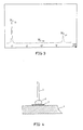
- Fig 2 shows a CVD system used to carry out the present example. It comprised the gas distribution system, the cold wall type chamber, the heating system, and the pumping system.
- the available gases are SiH4, WF6 (or MoF6, WCl6, MoCl6), He and Ar.
- Helium (He) is used as a carrier gas for metal halides.
- Argon is used to purge the chamber after the deposition is completed.
- Chamber (1) is a cold wall type water cooled (2) reactor made of stainless steel.
- the ceramic substrate, in this example AlN substrate (3) is set on a quartz glass plate (4) under which is a radient heater (5) with three infrared lamps, positionned in the middle of the chamber.
- the substrate temperature is measured by an infrared pyrometer (6).
- the chamber is pumped on by a turbo molecular pump (7) which is backed by one master booster pump (8) and a rotary pump (9).
- a pressure base around 10 ⁇ 6 Torr (1.33 x 10 ⁇ 4Pa) can be easily reached.
- a gate valve (10) isolates the chamber from the turbomolecular pump.
- a second pumping line bypassing the gate valve and containing a butterfly pressure controlling valve (11), a trap for detoxification (12), a master booster pump (13) and rotary pump (14) is operated during deposition.
- An Aluminium Nitride substrate (3) is set in the chamber (1) and when the pressure base is reached, typically around 10 ⁇ 6 Torr, the pumping line is exchanged for that used for deposition.
- Deposition time is 4 minutes.
- the pressure inside the chamber is set at 0.2 Torr. After the deposition was completed several purges were carried out with Ar gas.
- Nickel plating is carried out on a prescribed surface part (typically 2 mm by 2 mm) of a metallized layer 2 which is formed on the ceramic substrate 1. Thereafter, a stainless wire 3 of 0,8 mm diameter is soldered on the same by metal brazing 4. The stainless steel wire 3 is pulled up to measure the tensile strength of the metallized layer.
- an Alumina substrate is set in the reactor, then heated at 500°C.
- the deposition duration is two hours.
- the pressure inside the chamber is set at 0.4 Torr.
- the ratio SiH4/WF6 is maintained at substantially 0.60.
- the thickness of the layer is 94 microns, i.e. a deposition rate which is about 0.8 micron/min.
- This third example describes a deposition of Molybdenum layer containing some Silicon MoSi z on a ceramic substrate, e.g., in this case AIN.
- an Aluminium Nitride substrate is set in the reactor, then heated at 320°C. After temperature stabilization, the following gas mixture is injected in the reactor : 10 sccm of MoF6 22 sccm of SiH4 64 sccm of He
- the deposition time is 10 minutes.
- the pressure inside the chamber is set at 0.2 Torr.
- the ratio SiH4/MoF6 is maintained around 2,2.
- a qualitative analysis with a X-Ray analyser coupled with the SEM indicates the presence of Silicon in the deposited layer.
- a layer of 38 microns thick is obtained in 10 minutes, i.e. a deposition rate of about 3,8 micron/min.
Landscapes
- Chemical & Material Sciences (AREA)
- Engineering & Computer Science (AREA)
- Materials Engineering (AREA)
- Organic Chemistry (AREA)
- Ceramic Engineering (AREA)
- Inorganic Chemistry (AREA)
- General Chemical & Material Sciences (AREA)
- Chemical Kinetics & Catalysis (AREA)
- Mechanical Engineering (AREA)
- Metallurgy (AREA)
- Structural Engineering (AREA)
- Chemical Vapour Deposition (AREA)
- Ceramic Products (AREA)
Priority Applications (7)
| Application Number | Priority Date | Filing Date | Title |
|---|---|---|---|
| DE69032867T DE69032867T2 (de) | 1990-02-20 | 1990-02-20 | Metallisierte keramische Körper und Verfahren zu deren Herstellung |
| EP90400458A EP0443277B1 (fr) | 1990-02-20 | 1990-02-20 | Corps céramique métallisé et méthode pour le produire |
| AT90400458T ATE175179T1 (de) | 1990-02-20 | 1990-02-20 | Metallisierte keramische körper und verfahren zu deren herstellung |
| ES90400458T ES2127183T3 (es) | 1990-02-20 | 1990-02-20 | Cuerpo ceramico metalizado y metodo para fabricarlo. |
| KR1019910002464A KR910015718A (ko) | 1990-02-20 | 1991-02-13 | 금속 세라믹물체 및 그의 제조방법 |
| JP3045850A JPH04218674A (ja) | 1990-02-20 | 1991-02-18 | メタライズされたセラミック体およびその製造方法 |
| CA002036541A CA2036541A1 (fr) | 1990-02-20 | 1991-02-18 | Corps ceramique metallise et procede de fabrication |
Applications Claiming Priority (1)
| Application Number | Priority Date | Filing Date | Title |
|---|---|---|---|
| EP90400458A EP0443277B1 (fr) | 1990-02-20 | 1990-02-20 | Corps céramique métallisé et méthode pour le produire |
Publications (2)
| Publication Number | Publication Date |
|---|---|
| EP0443277A1 true EP0443277A1 (fr) | 1991-08-28 |
| EP0443277B1 EP0443277B1 (fr) | 1998-12-30 |
Family
ID=8205684
Family Applications (1)
| Application Number | Title | Priority Date | Filing Date |
|---|---|---|---|
| EP90400458A Expired - Lifetime EP0443277B1 (fr) | 1990-02-20 | 1990-02-20 | Corps céramique métallisé et méthode pour le produire |
Country Status (7)
| Country | Link |
|---|---|
| EP (1) | EP0443277B1 (fr) |
| JP (1) | JPH04218674A (fr) |
| KR (1) | KR910015718A (fr) |
| AT (1) | ATE175179T1 (fr) |
| CA (1) | CA2036541A1 (fr) |
| DE (1) | DE69032867T2 (fr) |
| ES (1) | ES2127183T3 (fr) |
Cited By (1)
| Publication number | Priority date | Publication date | Assignee | Title |
|---|---|---|---|---|
| CN118702507A (zh) * | 2024-08-14 | 2024-09-27 | 湖南省新化县鑫星电子陶瓷有限责任公司 | 一种氧化铝陶瓷基片的表面金属化工艺 |
Citations (5)
| Publication number | Priority date | Publication date | Assignee | Title |
|---|---|---|---|---|
| FR2344642A1 (fr) * | 1976-03-16 | 1977-10-14 | Thomson Csf | Procede de realisation de depots metalliques sur des supports en nitrure de bore |
| EP0157052A1 (fr) * | 1984-03-16 | 1985-10-09 | Genus, Inc. | Couche composite de tungstène et silicium à basse résistivité |
| EP0245934A2 (fr) * | 1986-05-15 | 1987-11-19 | Varian Associates, Inc. | Dépôt du silliciure métallique par LPCVD |
| EP0247783A2 (fr) * | 1986-05-29 | 1987-12-02 | Massachusetts Institute Of Technology | Méthode pour la déposition de métaux réfractaires |
| EP0305143A2 (fr) * | 1987-08-24 | 1989-03-01 | Fujitsu Limited | Procédé pour la formation sélective d'une couche conductrice |
-
1990
- 1990-02-20 AT AT90400458T patent/ATE175179T1/de active
- 1990-02-20 ES ES90400458T patent/ES2127183T3/es not_active Expired - Lifetime
- 1990-02-20 EP EP90400458A patent/EP0443277B1/fr not_active Expired - Lifetime
- 1990-02-20 DE DE69032867T patent/DE69032867T2/de not_active Expired - Fee Related
-
1991
- 1991-02-13 KR KR1019910002464A patent/KR910015718A/ko not_active Ceased
- 1991-02-18 CA CA002036541A patent/CA2036541A1/fr not_active Abandoned
- 1991-02-18 JP JP3045850A patent/JPH04218674A/ja active Pending
Patent Citations (5)
| Publication number | Priority date | Publication date | Assignee | Title |
|---|---|---|---|---|
| FR2344642A1 (fr) * | 1976-03-16 | 1977-10-14 | Thomson Csf | Procede de realisation de depots metalliques sur des supports en nitrure de bore |
| EP0157052A1 (fr) * | 1984-03-16 | 1985-10-09 | Genus, Inc. | Couche composite de tungstène et silicium à basse résistivité |
| EP0245934A2 (fr) * | 1986-05-15 | 1987-11-19 | Varian Associates, Inc. | Dépôt du silliciure métallique par LPCVD |
| EP0247783A2 (fr) * | 1986-05-29 | 1987-12-02 | Massachusetts Institute Of Technology | Méthode pour la déposition de métaux réfractaires |
| EP0305143A2 (fr) * | 1987-08-24 | 1989-03-01 | Fujitsu Limited | Procédé pour la formation sélective d'une couche conductrice |
Non-Patent Citations (1)
| Title |
|---|
| JOURNAL OF THE ELECTROCHEMICAL SOCIETY. vol. 135, no. 7, July 1988, MANCHESTER, NEW HAMP pages 1752 - 1757; G. A. West et al: "Chemical vapor deposiotion of Molybdenum Silicide" * |
Cited By (1)
| Publication number | Priority date | Publication date | Assignee | Title |
|---|---|---|---|---|
| CN118702507A (zh) * | 2024-08-14 | 2024-09-27 | 湖南省新化县鑫星电子陶瓷有限责任公司 | 一种氧化铝陶瓷基片的表面金属化工艺 |
Also Published As
| Publication number | Publication date |
|---|---|
| EP0443277B1 (fr) | 1998-12-30 |
| ES2127183T3 (es) | 1999-04-16 |
| DE69032867D1 (de) | 1999-02-11 |
| ATE175179T1 (de) | 1999-01-15 |
| JPH04218674A (ja) | 1992-08-10 |
| DE69032867T2 (de) | 1999-06-17 |
| CA2036541A1 (fr) | 1991-08-21 |
| KR910015718A (ko) | 1991-09-30 |
Similar Documents
| Publication | Publication Date | Title |
|---|---|---|
| EP0521405B1 (fr) | Composant évacuant la chaleur et dispositif semi-conducteur qui en est muni | |
| EP0516819B1 (fr) | Liaison directe de cuivre a des substrats en nitrure d'aluminium | |
| EP0991121A2 (fr) | Socle de montage améliorant le dissipation de chaleur pour empaquetage semiconducteur | |
| JPS62207789A (ja) | 窒化アルミニウム製基材の表面構造及びその製造法 | |
| JPH0516398B2 (fr) | ||
| JP2856782B2 (ja) | 低温cvdによる銅薄膜の形成方法 | |
| WO2002099879A1 (fr) | Dissipateur de chaleur et procede de fabrication correspondant | |
| WO1997005757A1 (fr) | Boitiers electroniques au diamant et a metal lie | |
| EP0443277B1 (fr) | Corps céramique métallisé et méthode pour le produire | |
| JPH0243700B2 (fr) | ||
| JPS58103156A (ja) | 半導体素子塔載用基板 | |
| EP0640039A1 (fr) | Metallisation en couche mince et brasage de nitrure d'aluminium | |
| JP3297571B2 (ja) | 静電チャック | |
| JP3569093B2 (ja) | 配線基板およびその製造方法 | |
| JP2000294696A (ja) | 電子回路用部材およびその製造方法 | |
| JPH03252382A (ja) | 窒化アルミニウム基板およびその製造方法 | |
| JPH05326767A (ja) | 放熱基板 | |
| JPS62182182A (ja) | 金属化面を有する窒化アルミニウム焼結体 | |
| JP2003068948A (ja) | 放熱基板の製造方法 | |
| JP2837049B2 (ja) | 複層セラミックスるつぼの製造方法 | |
| JPH04949B2 (fr) | ||
| Lux et al. | Diamond: a novel substrate for thick film technology | |
| JPH02283684A (ja) | 窒化アルミニウム焼結体の製造方法 | |
| JPH0453836B2 (fr) | ||
| JPH04337276A (ja) | 複層セラミックスヒ−タ− |
Legal Events
| Date | Code | Title | Description |
|---|---|---|---|
| PUAI | Public reference made under article 153(3) epc to a published international application that has entered the european phase |
Free format text: ORIGINAL CODE: 0009012 |
|
| 17P | Request for examination filed |
Effective date: 19900223 |
|
| AK | Designated contracting states |
Kind code of ref document: A1 Designated state(s): AT BE CH DE DK ES FR GB IT LI LU NL SE |
|
| 17Q | First examination report despatched |
Effective date: 19930615 |
|
| GRAG | Despatch of communication of intention to grant |
Free format text: ORIGINAL CODE: EPIDOS AGRA |
|
| GRAG | Despatch of communication of intention to grant |
Free format text: ORIGINAL CODE: EPIDOS AGRA |
|
| GRAH | Despatch of communication of intention to grant a patent |
Free format text: ORIGINAL CODE: EPIDOS IGRA |
|
| GRAH | Despatch of communication of intention to grant a patent |
Free format text: ORIGINAL CODE: EPIDOS IGRA |
|
| GRAA | (expected) grant |
Free format text: ORIGINAL CODE: 0009210 |
|
| AK | Designated contracting states |
Kind code of ref document: B1 Designated state(s): AT BE CH DE DK ES FR GB IT LI LU NL SE |
|
| PG25 | Lapsed in a contracting state [announced via postgrant information from national office to epo] |
Ref country code: CH Free format text: LAPSE BECAUSE OF FAILURE TO SUBMIT A TRANSLATION OF THE DESCRIPTION OR TO PAY THE FEE WITHIN THE PRESCRIBED TIME-LIMIT Effective date: 19981230 Ref country code: AT Free format text: LAPSE BECAUSE OF FAILURE TO SUBMIT A TRANSLATION OF THE DESCRIPTION OR TO PAY THE FEE WITHIN THE PRESCRIBED TIME-LIMIT Effective date: 19981230 Ref country code: NL Free format text: LAPSE BECAUSE OF FAILURE TO SUBMIT A TRANSLATION OF THE DESCRIPTION OR TO PAY THE FEE WITHIN THE PRESCRIBED TIME-LIMIT Effective date: 19981230 Ref country code: BE Free format text: LAPSE BECAUSE OF FAILURE TO SUBMIT A TRANSLATION OF THE DESCRIPTION OR TO PAY THE FEE WITHIN THE PRESCRIBED TIME-LIMIT Effective date: 19981230 Ref country code: LI Free format text: LAPSE BECAUSE OF FAILURE TO SUBMIT A TRANSLATION OF THE DESCRIPTION OR TO PAY THE FEE WITHIN THE PRESCRIBED TIME-LIMIT Effective date: 19981230 |
|
| REF | Corresponds to: |
Ref document number: 175179 Country of ref document: AT Date of ref document: 19990115 Kind code of ref document: T |
|
| REG | Reference to a national code |
Ref country code: CH Ref legal event code: EP |
|
| ET | Fr: translation filed | ||
| REF | Corresponds to: |
Ref document number: 69032867 Country of ref document: DE Date of ref document: 19990211 |
|
| ITF | It: translation for a ep patent filed | ||
| PG25 | Lapsed in a contracting state [announced via postgrant information from national office to epo] |
Ref country code: LU Free format text: LAPSE BECAUSE OF NON-PAYMENT OF DUE FEES Effective date: 19990220 |
|
| PG25 | Lapsed in a contracting state [announced via postgrant information from national office to epo] |
Ref country code: DK Free format text: LAPSE BECAUSE OF FAILURE TO SUBMIT A TRANSLATION OF THE DESCRIPTION OR TO PAY THE FEE WITHIN THE PRESCRIBED TIME-LIMIT Effective date: 19990330 Ref country code: SE Free format text: LAPSE BECAUSE OF FAILURE TO SUBMIT A TRANSLATION OF THE DESCRIPTION OR TO PAY THE FEE WITHIN THE PRESCRIBED TIME-LIMIT Effective date: 19990330 |
|
| REG | Reference to a national code |
Ref country code: ES Ref legal event code: FG2A Ref document number: 2127183 Country of ref document: ES Kind code of ref document: T3 |
|
| NLV1 | Nl: lapsed or annulled due to failure to fulfill the requirements of art. 29p and 29m of the patents act | ||
| REG | Reference to a national code |
Ref country code: CH Ref legal event code: PL |
|
| PLBE | No opposition filed within time limit |
Free format text: ORIGINAL CODE: 0009261 |
|
| STAA | Information on the status of an ep patent application or granted ep patent |
Free format text: STATUS: NO OPPOSITION FILED WITHIN TIME LIMIT |
|
| 26N | No opposition filed | ||
| PGFP | Annual fee paid to national office [announced via postgrant information from national office to epo] |
Ref country code: FR Payment date: 20010111 Year of fee payment: 12 |
|
| PGFP | Annual fee paid to national office [announced via postgrant information from national office to epo] |
Ref country code: GB Payment date: 20010118 Year of fee payment: 12 |
|
| PGFP | Annual fee paid to national office [announced via postgrant information from national office to epo] |
Ref country code: DE Payment date: 20010119 Year of fee payment: 12 |
|
| PGFP | Annual fee paid to national office [announced via postgrant information from national office to epo] |
Ref country code: ES Payment date: 20010207 Year of fee payment: 12 |
|
| REG | Reference to a national code |
Ref country code: GB Ref legal event code: IF02 |
|
| PG25 | Lapsed in a contracting state [announced via postgrant information from national office to epo] |
Ref country code: GB Free format text: LAPSE BECAUSE OF NON-PAYMENT OF DUE FEES Effective date: 20020220 |
|
| PG25 | Lapsed in a contracting state [announced via postgrant information from national office to epo] |
Ref country code: DE Free format text: LAPSE BECAUSE OF NON-PAYMENT OF DUE FEES Effective date: 20020903 |
|
| GBPC | Gb: european patent ceased through non-payment of renewal fee |
Effective date: 20020220 |
|
| PG25 | Lapsed in a contracting state [announced via postgrant information from national office to epo] |
Ref country code: FR Free format text: LAPSE BECAUSE OF NON-PAYMENT OF DUE FEES Effective date: 20021031 |
|
| REG | Reference to a national code |
Ref country code: FR Ref legal event code: ST |
|
| PG25 | Lapsed in a contracting state [announced via postgrant information from national office to epo] |
Ref country code: ES Free format text: LAPSE BECAUSE OF NON-PAYMENT OF DUE FEES Effective date: 20031122 |
|
| REG | Reference to a national code |
Ref country code: ES Ref legal event code: FD2A Effective date: 20031122 |
|
| PG25 | Lapsed in a contracting state [announced via postgrant information from national office to epo] |
Ref country code: IT Free format text: LAPSE BECAUSE OF NON-PAYMENT OF DUE FEES;WARNING: LAPSES OF ITALIAN PATENTS WITH EFFECTIVE DATE BEFORE 2007 MAY HAVE OCCURRED AT ANY TIME BEFORE 2007. THE CORRECT EFFECTIVE DATE MAY BE DIFFERENT FROM THE ONE RECORDED. Effective date: 20050220 |
|
| PG25 | Lapsed in a contracting state [announced via postgrant information from national office to epo] |
Ref country code: ES Free format text: LAPSE BECAUSE OF NON-PAYMENT OF DUE FEES Effective date: 20020228 |