EP0443521A1 - Lichtempfindliches Element für Elektrophotographie - Google Patents
Lichtempfindliches Element für Elektrophotographie Download PDFInfo
- Publication number
- EP0443521A1 EP0443521A1 EP91102351A EP91102351A EP0443521A1 EP 0443521 A1 EP0443521 A1 EP 0443521A1 EP 91102351 A EP91102351 A EP 91102351A EP 91102351 A EP91102351 A EP 91102351A EP 0443521 A1 EP0443521 A1 EP 0443521A1
- Authority
- EP
- European Patent Office
- Prior art keywords
- layer
- photosensitive member
- doped
- electrophotography
- photoconductive layer
- Prior art date
- Legal status (The legal status is an assumption and is not a legal conclusion. Google has not performed a legal analysis and makes no representation as to the accuracy of the status listed.)
- Withdrawn
Links
Images
Classifications
-
- G—PHYSICS
- G03—PHOTOGRAPHY; CINEMATOGRAPHY; ANALOGOUS TECHNIQUES USING WAVES OTHER THAN OPTICAL WAVES; ELECTROGRAPHY; HOLOGRAPHY
- G03G—ELECTROGRAPHY; ELECTROPHOTOGRAPHY; MAGNETOGRAPHY
- G03G5/00—Recording-members for original recording by exposure, e.g. to light, to heat or to electrons; Manufacture thereof; Selection of materials therefor
- G03G5/02—Charge-receiving layers
- G03G5/04—Photoconductive layers; Charge-generation layers or charge-transporting layers; Additives therefor; Binders therefor
- G03G5/08—Photoconductive layers; Charge-generation layers or charge-transporting layers; Additives therefor; Binders therefor characterised by the photoconductive material being inorganic
- G03G5/082—Photoconductive layers; Charge-generation layers or charge-transporting layers; Additives therefor; Binders therefor characterised by the photoconductive material being inorganic and not being incorporated in a bonding material, e.g. vacuum deposited
- G03G5/08214—Silicon-based
- G03G5/08278—Depositing methods
-
- G—PHYSICS
- G03—PHOTOGRAPHY; CINEMATOGRAPHY; ANALOGOUS TECHNIQUES USING WAVES OTHER THAN OPTICAL WAVES; ELECTROGRAPHY; HOLOGRAPHY
- G03G—ELECTROGRAPHY; ELECTROPHOTOGRAPHY; MAGNETOGRAPHY
- G03G5/00—Recording-members for original recording by exposure, e.g. to light, to heat or to electrons; Manufacture thereof; Selection of materials therefor
- G03G5/02—Charge-receiving layers
- G03G5/04—Photoconductive layers; Charge-generation layers or charge-transporting layers; Additives therefor; Binders therefor
- G03G5/08—Photoconductive layers; Charge-generation layers or charge-transporting layers; Additives therefor; Binders therefor characterised by the photoconductive material being inorganic
- G03G5/082—Photoconductive layers; Charge-generation layers or charge-transporting layers; Additives therefor; Binders therefor characterised by the photoconductive material being inorganic and not being incorporated in a bonding material, e.g. vacuum deposited
- G03G5/08214—Silicon-based
- G03G5/08221—Silicon-based comprising one or two silicon based layers
Definitions
- This invention relates to a photosensitive member for electrophotography, and more particularly to a photosensitive member for electrophotography of negative charge type which is useful as a photoreceptor of duplicator.
- a photosensitive member for electrophotography made of an a-Si (amorphous silicon) having excellent properties of high photoconductivity and high hardness and being non-pollutive has been given special notices.
- the a-Si photosensitive member is generally fabricated ; by plasma CVD process in such manner that a source gas such as monosilane (SiH4) or disilane (Si2H6) is introduced into a vacuum chamber and applied with a radio frequency (rf) power to form a glow discharge, so that the source gas is decomposed to deposit a photoconductive layer mainly of a-Si on a substrate; or by reactive sputtering process in such manner that a silicon wafer is used in place of the above source gas as a target for sputtering and H2, He, Ar or like gas is introduced and applied with a rf power to form a glow discharge so as to sputter the target Si wafer, thereby depositing a photoconductive layer mainly of a-Si on the substrate.
- the a-Si photoconductive layer fabricated above usually contains hydrogen of 10 to 30 at.% and exhibits a slightly n-type conduction even when not added, i.e., non-doped, with a conductivity-controlling impurity (for example, B (boron) of III group element, P (phosphorus) of V group element and the like). Since the electron as a carrier is superior in mobility than the hole, the a-Si photoconductive layer inherently exhibits a high photoconductivity but shows a relatively high dark conductivity such as 10 ⁇ 9 to 10 ⁇ 10 S/cm.
- the photoconductive layer having such conductivities, when applied as it is to a photosensitive member for electrophotography of negative charge type, is inferior in charge acceptance and dark decay characteristic (charge retentivity) due to the relatively high dark conductivity.
- an a-Si layer can be fabricated by ECR process (electron cyclotron resonance process) (USP 4,532,199). Also, we have proposed that an a-SiGe layer, an a-Si/a-SiGe composite layer or an a-SiX layer (wherein X represents C, N or O) each fabricated by ECR process can suitably be applied as a photoconductive layer of photosensitive member for electrophotography mainly of positive charge type (US patent application serial Nos. 368,807, 372,019 and 369,473). However, it is still not known of fabricating by ECR process an a-Si photoconductive layer in the photosensitive member for electrophotography of negative charge type.
- a photosensitive member for electrophotography comprising an intermediate layer, a photoconductive layer and a surface protecting layer each deposited upwardly in this order on a conductive substrate, wherein the photoconductive layer comprises a non-doped a-Si layer made of an amorphous silicon containing hydrogen and/or halogen of 40 at.% or more.
- the invention is based on the inventor's discovery of such a fact that using the non-doped a-Si layer as defined above as a photoconductive layer of the photosensitive member of negative charge type enables the photosensitive member to exhibit an excellent charge acceptance and dark decay characteristic.
- the photoconductive layer can simply be fabricated without doping impurity such as B or P or adding chemical modifier such as C, N or O. Therefore, in addition to the merit of enabling the characteristic of a non-doped a-Si to be developed for the photoconductive layer, the photosensitive member can take such an advantage in production of being efficiently fabricated with higher photoconductivity and lower dark conductivity.
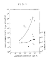
- Fig. 1 is a diagram showing a property of an a-Si layer of the present invention prepared by ECR process.
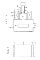
- Fig. 2 is a cross sectional view showing a structure of the photosensitive member of the present invention.
- Fig. 3 is a schematic diagram of a deposition apparatus according to ECR process.
- the conductive substrate may employ conventional materials available in the art, for example, metals such as Al, Cr, Mo, Au, Ir, Nb, Ta, Pt, Pd and the like, or a plate made from alloys provided from those metals. Also, available are a film or a sheet made of synthetic resins such as polyester, polyethylene, cellulose acetate, polypropylene and the like, or a sheet made of glass, ceramic and the like, the surfaces of the film or sheet being coated with a conductive layer.
- the substrate may be formed in any shape suitable for the purpose (for example, a drum and the like) and is not limited to a particular shape.
- the intermediate layer which prevents the injection of holes from the conductive substrate to the photoconductive layer is first fabricated on the above conductive substrate.
- the intermediate layer may be a conventional a-Si layer doped with a n-type impurity (for example, phosphorus) optionally containing a chemical modifier.
- a doped a-Si layer (n-type impurity of 1016 to 1021/cm3) having a thickness of 0.2 to 20 ⁇ m fabricated, for example, in accordance with a conventional PCVD process or sputtering process, or ECR process.
- the photoconductive layer is deposited on the intermediate layer, comprising an a-Si layer which contains hydrogen and/or halogen of 40 at.% or more and not doped with any impurity such as B or P, or a chemical modifier and the like.
- the non-doped a-Si layer defined above can be prepared in accordance with ECR process using as a source gas, for example, SiH4, Si2H6, SiF4, SiCl4, SiHCl3, SiH2Cl2 and the like, solely or in combination. It is preferable that an applied microwave power in ECR process be 0.5 to 5 kW, source gas flow be 50 to 500 sccm, and the gas pressure under deposition be 10 ⁇ 5 to 10 ⁇ 2 Torr. Also, it is preferable that the thickness of the non-doped a-Si layer be 10 to 50 ⁇ m and the hydrogen and/or halogen content be 40 to 60 at.%, most preferably be 42 to 55 at.%.
- a source gas for example, SiH4, Si2H6, SiF4, SiCl4, SiHCl3, SiH2Cl2 and the like, solely or in combination. It is preferable that an applied microwave power in ECR process be 0.5 to 5 kW, source gas flow be 50 to 500 sccm
- the surface protecting layer is fabricated on the photoconductive layer to complete the photosensitive member of the present invention.
- the surface protecting layer may be preferably provided for protecting the photosensitive member from physical or chemical damage such as corona discharge, and may preferably be an a-Si layer added with a chemical modifier such as C, N, O and the like, i.e., a-SiC, a-SiN or a-SiO layer and the like.
- the surface protecting layer can be fabricated in accordance with a conventional PCVD process or ECR process using a silicon source gas similarly with the aforesaid process and a chemical modifier source gas such as hydrocarbons (for example, CH4, C2H6, C3H8, and the like), NH3, O2, CO2 and the like. It is preferable that the concentration of the chemical modifier element be 10 to 200 at.% and the thickness of the surface protecting layer be 0.1 to 10 ⁇ m.
- the hydrogen and/or halogen content in an a-Si layer fabricated in accordance with a conventional plasma CVD process or reactive sputtering process is generally 10 to 30 at.%, but that in an a-Si layer fabricated in accordance with ECR process is possibly around 40 at.% to 60 at.%.
- ECR process employs the formation of plasma based on the resonance between electron and microwave in magnetic field to make deposition in the presence of the Si source gas and has the following features.
- the a-Si layer obtained by ECR process has the following characteristics.
- the photosensitive member for electrophotography having an excellent charge acceptance and dark decay characteristic can be fabricated without decreasing the inherent excellent photoconductivity of a-Si.
- Fig. 3 shows a schematic diagram of a deposition apparatus according to ECR process.
- the deposition apparatus comprises a plasma formation chamber 11 and a deposition chamber 12 wherein film-deposition is made.
- the plasma formation chamber 11 and the deposition chamber 12 are evacuated by a turbo-molecular pump and a rotary oil pump (each not shown).
- the plasma formation chamber 11 constructs a cavity resonator, to which microwave power with a frequency of 2.45 GHz is introduced through a rectangular waveguide 14 and a microwave introducing window 15 made of quartz glass. H2, N2 and an inert gas such as He, Ar or the like are introduced into the plasma formation chamber 11 through a gas tube 17.
- a magnetic coil 16 is provided around the plasma formation chamber 11 to form a magnetic field satisfying ECR conditions in a proper region inside the plasma formation chamber 11 and form divergent magnetic field by which excited plasma is extracted into the deposition chamber 12 through a plasma extraction window 13.
- a conductive substrate 18 for a photosensitive member which is to be situated in the deposition chamber 12 is made of a conductive material, for example, Al and in a cylindrical shape in this example. The cylindrical substrate 18 is supported rotatably by a supporting means (not shown) to uniformly deposit a film on its surface.
- the deposition chamber 12 is provided with a gas inlet tube 19 for introducing a source gas such as SiH4 or the like.
- the deposition process is conducted in the following manner.
- the plasma formation chamber 11 and the deposition chamber 12 are first evacuated, then H2, N2 and an inert gas such as He, Ar or the like are introduced into the plasma formation chamber 11 and a source gas into the deposition chamber 12.
- the source gases include silicon compounds having either hydrogen or halogen or both of them such as SiH4, Si2H6, SiF4, SiCl4, SiH2Cl2 and the like.
- gas pressure is set at about 10 ⁇ 3 to 10 ⁇ 4 Torr.
- a current is supplied to the magnetic coil 16 to form a magnetic field, and microwave power is introduced into the plasma formation chamber 11 to form plasma.
- Excited plasma is introduced into the deposition chamber 12 through the plasma extraction window 13 to deposit a film on the substrate 18.
- the substrate 18 is rotated during deposition thereby enabling a uniform film-formation. Uniformity of deposition may be improved by changing the shape of the plasma extraction window 13 and a distance between the plasma extraction window 13 and the substrate 18.
- Fig. 1 shows a relationship between the hydrogen content in the a-Si film and the photoconductivity ( ⁇ ) and dark conductivity.
- the a-Si film fabricated according to ECR process exhibits a lower dark conductivity than those provided by the conventional process.
- the dark conductivity shown by the conventional a-Si film when not doped with impurity is 10 ⁇ 9 to 10 ⁇ 10 S/cm and that shown by the ECR a-Si film of the present invention is 10 ⁇ 11 to 10 ⁇ 12 S/cm.
- the hydrogen content is set to be 40 at.% or more
- the ECR a-Si film exhibits a best photoconductivity 10 ⁇ 7 to 10 ⁇ 6cm2/V which is the same as the conventional a-Si film with the hydrogen content of 10 to 30 at.%.
- the a-Si film having the favorable properties above is not able to be prepared by the conventional deposition methods and is sufficiently usable as a photoconductive layer of a photosensitive member for electrophotography of negative charge type, providing a good contrast in image on the basis of the large difference between the dark conductivity and photoconductivity.
- the hydrogen content in the a-Si layer is over 60 at.%, hydrogen may exists therein in SiH2 polymer configuration, causing the photoconductivity to be lowered. Hence, it is preferable that the hydrogen content be set to 40 to 60 at.%.
- the favorable dark conductivity and photoconductivity were observed when the a-Si film contains halogen as well as or in place of hydrogen.
- Fig. 2 shows a structure of an photosensitive member for electrophotography which we practically prepared.
- the photosensitive member has an intermediate layer 2 (4 ⁇ m thick ), a photoconductive layer 3 (35 ⁇ m) and a surface protecting layer 4 (0.5 ⁇ m) each deposited on a conductive substrate 1 made of aluminium and the like.
- the intermediate layer 2, photoconductive layer 3 and surface protecting layer 4 are formed with the depositing apparatus as aforesaid.
- the following table shows the deposition conditions for each layer.
- An electrophotographic property as a negative charge type photosensitive member was measured on the above member to obtain a result that the photosensitive member has a sufficient charge acceptance and dark decay characteristic and exhibits a favorable photosensitivity superior to the conventional member, with having a less residual potential.
- the photosensitive member was mounted in a commercially available duplicator for an estimation of image quality and could provide a favorable image without having fogging.
- SiH2Cl2, SiCl4, SiF4 and the like may be used as a source gas to provide a similar result with the above.
- the present invention provides an advantage that the non-doped a-Si which is inherently superior in photoconductivity is made use of without deteriorating the photoconductivity due to the addition, for example, of boron or like.
- adjusting the hydrogen and/or halogen content in the a-Si to 40 at.% or more decreases the dark conductivity thereby providing a sufficient charge acceptance and dark decay characteristic for a photosensitive member.
- the photosensitive member of an a-Si layer having hydrogen and/or halogen content of 40 at.% or more with a favorable property cannot be obtained by the conventional PCVD or reactive sputtering process but is realized by ECR process.
- ECR process eliminates such problems in the conventional depositing processes of (1) a lower deposition rate, (2) a lower gas usage efficiency, and (3) production of polymeric powder of (SiH2) n forms defects in a deposited layer. Further, the high quality a-Si layer can be obtained without heating the substrate, and cost reduction and improvement of productivity can be facilitated.
Landscapes
- Chemical & Material Sciences (AREA)
- Inorganic Chemistry (AREA)
- Physics & Mathematics (AREA)
- General Physics & Mathematics (AREA)
- Photoreceptors In Electrophotography (AREA)
Applications Claiming Priority (2)
| Application Number | Priority Date | Filing Date | Title |
|---|---|---|---|
| JP40718/90 | 1990-02-20 | ||
| JP2040718A JPH03242653A (ja) | 1990-02-20 | 1990-02-20 | 電子写真感光体 |
Publications (1)
| Publication Number | Publication Date |
|---|---|
| EP0443521A1 true EP0443521A1 (de) | 1991-08-28 |
Family
ID=12588379
Family Applications (1)
| Application Number | Title | Priority Date | Filing Date |
|---|---|---|---|
| EP91102351A Withdrawn EP0443521A1 (de) | 1990-02-20 | 1991-02-19 | Lichtempfindliches Element für Elektrophotographie |
Country Status (3)
| Country | Link |
|---|---|
| US (1) | US5100749A (de) |
| EP (1) | EP0443521A1 (de) |
| JP (1) | JPH03242653A (de) |
Families Citing this family (2)
| Publication number | Priority date | Publication date | Assignee | Title |
|---|---|---|---|---|
| US5239397A (en) * | 1989-10-12 | 1993-08-24 | Sharp Kabushiki | Liquid crystal light valve with amorphous silicon photoconductor of amorphous silicon and hydrogen or a halogen |
| JPH0572783A (ja) * | 1991-04-12 | 1993-03-26 | Fuji Xerox Co Ltd | 電子写真感光体 |
Citations (3)
| Publication number | Priority date | Publication date | Assignee | Title |
|---|---|---|---|---|
| US4698288A (en) * | 1985-12-19 | 1987-10-06 | Xerox Corporation | Electrophotographic imaging members having a ground plane of hydrogenated amorphous silicon |
| DE3717727A1 (de) * | 1987-05-26 | 1988-12-08 | Licentia Gmbh | Elektrofotografisches aufzeichnungsmaterial und verfahren zu seiner herstellung |
| EP0336700A2 (de) * | 1988-04-04 | 1989-10-11 | Sharp Kabushiki Kaisha | Elektrophotographisches lichtempfindliches Element |
Family Cites Families (4)
| Publication number | Priority date | Publication date | Assignee | Title |
|---|---|---|---|---|
| JPS56115573A (en) * | 1980-02-15 | 1981-09-10 | Matsushita Electric Ind Co Ltd | Photoconductive element |
| JPS5752180A (en) * | 1980-09-12 | 1982-03-27 | Canon Inc | Photoconductive member |
| JPS5756847A (en) * | 1980-09-24 | 1982-04-05 | Canon Inc | Photoconductive member |
| JPH07117764B2 (ja) * | 1988-04-04 | 1995-12-18 | シャープ株式会社 | 電子写真感光体の製造方法 |
-
1990
- 1990-02-20 JP JP2040718A patent/JPH03242653A/ja active Pending
-
1991
- 1991-02-19 US US07/656,430 patent/US5100749A/en not_active Expired - Lifetime
- 1991-02-19 EP EP91102351A patent/EP0443521A1/de not_active Withdrawn
Patent Citations (3)
| Publication number | Priority date | Publication date | Assignee | Title |
|---|---|---|---|---|
| US4698288A (en) * | 1985-12-19 | 1987-10-06 | Xerox Corporation | Electrophotographic imaging members having a ground plane of hydrogenated amorphous silicon |
| DE3717727A1 (de) * | 1987-05-26 | 1988-12-08 | Licentia Gmbh | Elektrofotografisches aufzeichnungsmaterial und verfahren zu seiner herstellung |
| EP0336700A2 (de) * | 1988-04-04 | 1989-10-11 | Sharp Kabushiki Kaisha | Elektrophotographisches lichtempfindliches Element |
Also Published As
| Publication number | Publication date |
|---|---|
| US5100749A (en) | 1992-03-31 |
| JPH03242653A (ja) | 1991-10-29 |
Similar Documents
| Publication | Publication Date | Title |
|---|---|---|
| CA1166505A (en) | Electrophotographic photosensitive layer including amorphous silicon containing hydrogen | |
| US4702934A (en) | Electrophotographic photosensitive member, process and apparatus for the preparation thereof | |
| GB2148328A (en) | Chemical vapour deposition process | |
| JPH0360917B2 (de) | ||
| US5582648A (en) | Apparatus for preparing a functional deposited film by microwave plasma chemical vapor deposition | |
| US4943503A (en) | Amorphous silicon photoreceptor | |
| US5338580A (en) | Method of preparation of functional deposited film by microwave plasma chemical vapor deposition | |
| EP0443521A1 (de) | Lichtempfindliches Element für Elektrophotographie | |
| JPH081895B2 (ja) | 非晶質シリコン膜の形成方法 | |
| JPS6348057B2 (de) | ||
| US5011759A (en) | Semiconductor element and method of forming same and article in which said element is used | |
| JP3010199B2 (ja) | 光導電体 | |
| JP2650050B2 (ja) | 薄膜形成法 | |
| JP3102725B2 (ja) | 光受容部材及びその製造方法 | |
| US5009977A (en) | Photosensitive member for electrophotography having amorphous silicon | |
| US4971878A (en) | Amorphous silicon photosensitive member for use in electrophotography | |
| US4913995A (en) | Amorphous silicon electrophotographic photoreceptor with an intermediate gradient layer and its method of preparation | |
| US4990423A (en) | Photosensitive member for electrophotography | |
| JPH0647738B2 (ja) | プラズマcvd法による堆積膜形成方法 | |
| JPH0315739B2 (de) | ||
| JP2668407B2 (ja) | 電子写真用像形成部材 | |
| JP3320228B2 (ja) | 電子写真用光受容部材の製造方法 | |
| JP3402952B2 (ja) | 堆積膜形成方法及び堆積膜形成装置 | |
| JPH087448B2 (ja) | 電子写真感光体の製造方法 | |
| JPH07117764B2 (ja) | 電子写真感光体の製造方法 |
Legal Events
| Date | Code | Title | Description |
|---|---|---|---|
| PUAI | Public reference made under article 153(3) epc to a published international application that has entered the european phase |
Free format text: ORIGINAL CODE: 0009012 |
|
| AK | Designated contracting states |
Kind code of ref document: A1 Designated state(s): DE FR GB |
|
| 17P | Request for examination filed |
Effective date: 19911126 |
|
| 17Q | First examination report despatched |
Effective date: 19940726 |
|
| STAA | Information on the status of an ep patent application or granted ep patent |
Free format text: STATUS: THE APPLICATION IS DEEMED TO BE WITHDRAWN |
|
| 18D | Application deemed to be withdrawn |
Effective date: 19951209 |