EP0444433A2 - Circuit pour trigger de Schmitt opto-électronique - Google Patents
Circuit pour trigger de Schmitt opto-électronique Download PDFInfo
- Publication number
- EP0444433A2 EP0444433A2 EP91101428A EP91101428A EP0444433A2 EP 0444433 A2 EP0444433 A2 EP 0444433A2 EP 91101428 A EP91101428 A EP 91101428A EP 91101428 A EP91101428 A EP 91101428A EP 0444433 A2 EP0444433 A2 EP 0444433A2
- Authority
- EP
- European Patent Office
- Prior art keywords
- stage
- output
- transistor
- amplifier stage
- differential amplifier
- Prior art date
- Legal status (The legal status is an assumption and is not a legal conclusion. Google has not performed a legal analysis and makes no representation as to the accuracy of the status listed.)
- Granted
Links
Images
Classifications
-
- H—ELECTRICITY
- H03—ELECTRONIC CIRCUITRY
- H03K—PULSE TECHNIQUE
- H03K17/00—Electronic switching or gating, i.e. not by contact-making and –breaking
- H03K17/51—Electronic switching or gating, i.e. not by contact-making and –breaking characterised by the components used
- H03K17/78—Electronic switching or gating, i.e. not by contact-making and –breaking characterised by the components used using opto-electronic devices, i.e. light-emitting and photoelectric devices electrically- or optically-coupled
- H03K17/795—Electronic switching or gating, i.e. not by contact-making and –breaking characterised by the components used using opto-electronic devices, i.e. light-emitting and photoelectric devices electrically- or optically-coupled controlling bipolar transistors
-
- H—ELECTRICITY
- H03—ELECTRONIC CIRCUITRY
- H03K—PULSE TECHNIQUE
- H03K3/00—Circuits for generating electric pulses; Monostable, bistable or multistable circuits
- H03K3/02—Generators characterised by the type of circuit or by the means used for producing pulses
- H03K3/023—Generators characterised by the type of circuit or by the means used for producing pulses by the use of differential amplifiers or comparators, with internal or external positive feedback
- H03K3/0233—Bistable circuits
- H03K3/02337—Bistables with hysteresis, e.g. Schmitt trigger
Definitions
- the invention relates to a circuit arrangement for an Opto-Schmitt trigger according to the preamble of claim 1.
- Opto-Schmitt triggers are used as radiation receivers in the form of individual components or in sensors, for example in fork / reflex light barriers or in opto-isolators.
- the optical receiving part usually a photodiode, is used to convert the optical radiation into an electrical signal, the electronic part - amplifier and Schmitt trigger - for processing the input signal; the output signal is output at the circuit output.
- the output signal is modified; when a second threshold value is reached, it returns to the original value. Due to the Schmitt trigger function, pulse formation takes place, and due to the built-in hysteresis, interference signals are largely suppressed.
- the invention is based on the object of specifying an advantageous circuit arrangement for an Opto-Schmitt trigger. This is achieved according to the invention in that the amplifier stage contains a transimpedance amplifier stage, a differential amplifier stage, a first reference network and a compensation element, that the Schmitt trigger stage consists of a differential amplifier stage, a second reference network and a positive feedback branch, and that the output signal at the circuit output of the Output stage is present.
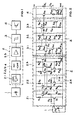
- the individual circuit components of the Opto-Schmitt trigger circuit according to the invention are listed in the block diagram of FIG. 1; these components are also shown in FIGS. 2, 4 and 6 as schematic blocks.
- the monolithically integrated Opto-Schmitt trigger IC consists of an integrated photodiode 1, a two-stage amplifier 2 (transimpedance amplifier 2.1, differential amplifier 2.3, reference network 2.2 and compensation element 2.4) with a downstream Schmitt trigger stage 3 and the circuit output 4.
- the optical input signal is first converted into an electrical signal (photocurrent).
- the transimpedance amplifier 2.1 converts the photo current into a voltage swing, which is amplified by the differential amplifier 2.3.
- pulse shaping is carried out with the inclusion of a hysteresis;
- a TTL-compatible signal is available at the output transistor of the open collector output 4, for example.
- the transimpedance amplifier stage is simulated according to the invention by the first reference network and the photo-receiving element by a compensation element.
- the switch-on and switch-off thresholds of the Schmitt trigger stage can be individually adapted to different basic signal levels by changing resistances. However, the switch-off threshold must not fall below a certain minimum value, since safe switch-off must also be ensured in the event of parameter fluctuations or specimen scatter of the components.
- the switch-on sensitivity of the Schmitt trigger can be changed as a function of the temperature. The sensitivity is preferably changed such that it increases with increasing temperature; this serves to partially compensate for the temperature influence on the optical path - for example in opto-couplers between the LED and the photodiode.
- the compensation capacitor is replaced by a further photodiode - the difference between two photodiode signals can be formed.
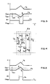
- Example 1 "active-LOW" version (Fig. 2 and 3)
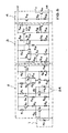
- the incident optical radiation is detected by the photodiode 1 and converted into a voltage signal by the conversion resistor R3 of the transimpedance amplifier stage 2.1.
- the transimpedance amplifier stage 2.1 contains in addition to the resistor R3, the resistors R1, R5 and R11 and the transistors Q1 and Q3. Due to the circuit arrangement, the input time constant is kept small, so that the operating frequency of the circuit is high.
- the cathode-side output of the photodiode 1 is connected to both the resistor R3 and the base of the transistor Q1; the collector of the transistor Q1 is connected to both the base of the transistor Q3 and to a terminal of the resistor R1.
- the emitter of the transistor Q3 leads both to the resistor R11, the other terminal of which is connected to the two resistors R3 and R5, and to the base terminal of the first transistor Q5 of the differential amplifier in the differential amplifier stage 2.3.
- the anode of the photodiode 1, the emitter of the transistor Q1 and the second terminal of the resistor R5 are connected to ground potential (GND), the collector of the transistor Q3 and the second terminal of the resistor R1 to the supply voltage (for example + 5V).
- the reference network 2.2 is constructed analogously to the transimpedance amplifier stage 2.1, the transistors Q2 and Q4 of the reference network, the transistors Q1 and Q3 of the transimpedance amplifier, the resistors R2, R6 and R12 of the reference network correspond to the resistors R1, R5 and R11 of the transimpedance amplifier.
- the emitter of the transistor Q4 is connected to the base of the second transistor Q6 of the differential amplifier in the differential amplifier stage 2.3.
- the dynamic properties of the transimpedance amplifier stage 2.1 are influenced by the photo receiving element, for example the photodiode 1;
- the photo-receiving element 1 is simulated by the compensation element 2.4, for example by the compensation capacitor C.
- a dynamic synchronization of the base potentials of the two differential amplifier transistors Q5 and Q6 is thus achieved.
- This consists of the transistors Q5, Q6, Q7 and Q9, the diode Q8, and the resistors R7 to R10 and R13 to R15.
- the two transistors Q5 and Q6 form the actual differential amplifier, the bases of which, as described above, are driven by the transimpedance amplifier stage 2.1 or the reference network 2.2 and with the aid of the compensation element 2.4 in static and dynamic synchronism.
- the emitters of the transistors Q5 and Q6 are on the resistors R9 and R10 to the common current source, the collector of transistor Q7 connected; this is driven by the voltage divider R8, R14 and Q8, the base of the transistor Q7 being connected to the anode of the diode Q8 and the resistor R8.
- the emitter of the transistor Q7 is connected to ground via the resistor R13, the cathode of the diode Q8 via the resistor R14.
- the output signal of the differential amplifier stage 2.3 is output via the tap on the collector of the transistor Q5 and the emitter follower transistor Q9 and its emitter resistor R15 at the emitter of the transistor Q9 as the voltage U3.
- the collector resistor R7 of the transistor Q5, the second terminal of the resistor R8 and the collectors of the transistors Q6 and Q9 are connected to the supply voltage.
- the second connection of the emitter resistor R15 is connected to ground potential.
- the two transistors Q10 and Q11 whose emitters are connected to each other and to the collector of the transistor Q12 working as a current source, form the "actual Schmitt trigger".
- the collector of the transistor Q10 is direct, the collector of the transistor Q11 via the collector resistor R21 connected to the supply voltage.
- the base of the transistor Q12 is driven by the voltage divider R19, diode Q13 and R17, the base being connected to a terminal of the resistor R19 and to the anode of the diode Q13; the cathode of the diode Q13 is connected to the resistor R17.
- the second terminal of the resistor R19 is connected to the supply voltage, the resistor R17 and the emitter resistor R18 of the transistor Q12 to ground.
- the base potential of the transistor Q10 is driven by the voltage output of the differential amplifier stage 2.3 (emitter of the transistor Q9), the base potential of the transistor Q11 from the emitter of the transistor Q14 of a reference network 3.2.
- the tap on the collector of the transistor Q11 is connected to the base of the transistor Q17 in the positive feedback branch 3.3.
- the reference network 3.2 provides the reference potential for the base of the transistor Q11 and consists of the voltage divider R22, diode Q15 and R23 and the emitter follower transistor Q14 with the emitter resistor R20.
- the collector of the emitter follower transistor Q14 and the second terminal of the resistor R22 are connected to the supply voltage, the second terminal of the resistor R23, the other terminal of which is connected to the cathode of the diode Q15, to ground potential.
- the anode of the diode Q15, the first terminal of the resistor R22 and the base of the transistor Q14 are connected to the node K1, to which the anode of the diode Q16 of the positive feedback branch 3.3 is connected.
- the positive feedback in the Schmitt trigger stage 3 is achieved in the positive feedback branch 3.3 using the emitter follower transistor Q1 Transistor, the divider from R2 aus, R25, the transistor Q19, its collector resistor R2widerstand and the diode Q16 and the resistor R29.
- the anode of the diode Q16 is connected to the base of the transistor Q14, the resistor R22 and the anode of the diode Q15, the cathode of Q16 to the resistor R29, whose other connection to both the resistor R26, to the collector of the transistor Q19 and to the base of the emitter follower transistor Q18 is connected.
- the base of the transistor Q19 in turn is connected to the second terminal of the resistor R24 and to the resistor R25, the second terminal and the emitter of the transistor Q19 is connected to ground potential.
- the second connection of the resistor R26 is connected to the supply voltage.
- the switch-on threshold of the Schmitt trigger 3 is - in the "active-LOW" version described here - set by the resistance R29 and the internal resistance of the network R22, Q15 and R23; it can be changed by varying the resistance R29 without touching the switch-off threshold.
- the switch-off threshold must not be changed arbitrarily or unintentionally, so that the switch-off condition for the Opto-Schmitt trigger remains guaranteed.
- the diode path Q16 with the resistor R29 in the blocking state is determined by the point P2, so that the typical hysteresis curve of a Schmitt trigger is achieved.
- the voltage U2 drops so far (point P2) that the transistor Q10 changes to the conductive state.
- the transistor Q10 takes over the full current of the current source Q12, the transistor Q11 blocks.
- the emitter follower Q17 and the voltage divider R24 and R25 causes the transistor Q19 to go into the conductive state; thereby the collector potential of the transistor Q19 drops sharply (approximately to the collector-emitter residual voltage U CE rest ). Consequently, the branch diode Q16 and R29 conductive, which in turn the voltage divider R22, Q15, R23 is loaded by this branch, so that the base potential of the transistor Q14 or the base potential of the transistor Q11 drops to the point P1.
- the voltage U3 has the switch-U one below. The hysteresis is given by the voltage difference between the turn-.DELTA.U a U (point P1) and the switch-off of U (point P2).
- the point P1 By varying the resistance R29 the point P1, ie the switch-on threshold of the Opto-Schmitt trigger, can be changed individually without the point P2, ie the switch-off threshold, being changed.
- the point P2, ie the switch-off threshold of the Opto-Schmitt trigger By varying the resistances R22 and R23, the point P2, ie the switch-off threshold of the Opto-Schmitt trigger, can be shifted.
- This consists of the emitter follower Q18, the base of which is connected to the resistors R26, R29 and the collector of the transistor Q19, the voltage divider R27, R28 and, for example, the open collector output transistor Q20.
- the emitter of the transistor Q18 is connected to the resistor R27, the base of the transistor Q20 to the tap of the voltage divider R27, R28; the collector of the transistor Q18 is connected to the supply voltage, the second terminal of the resistor R28 and the emitter of the transistor Q20 to ground.
- the voltage curve at the output of the Opto-Schmitt trigger (U4) is shown in the bottom curve of FIG.
- the HIGH state being given, for example, by the supply voltage 5 V and the LOW state by the residual voltage U rest of the output transistor Q20 .
- point P1 blocks the transistor Q19 according to the above statements, so that the transistor Q10 leads the output transistor Q20; the output is thus in the LOW state.
- the open collector output can be connected to the supply voltage via a load resistor, whereby the load resistor R L can be specified individually for the respective application. After falling below the minimum irradiation (point P2), the transistor Q19 is conductive, so that the transistor Q18 and thus the transistor Q20 blocks; the output then goes high.
- any other circuit outputs can be used, depending on the requirements and possible applications.
- Example 2 "active HIGH” version (Fig. 4 and 5)
- the output transistor switches to the HIGH state when a photocurrent is generated, ie the circuit output 4 takes the HIGH state when there is light excitation and the LOW state when the excitation is removed a.
- the required circuit is modified only slightly in the differential amplifier part 2.3 compared to the "active LOW" version in FIG. 2; the resistance R7 is no longer, as in Figure 2, the collector resistance of the transistor Q5, but as shown in Figure 4, the collector resistance of the transistor Q6.
- the potential tap of the two transistors is just being exchanged; consequently, the voltage U3 at the amplifier output is exactly opposite to that of the "active-LOW version.
- the user can therefore choose either the “active-LOW” or the “active-HIGH” version.
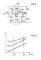
- Example 3 Targeted temperature-dependent switch-on threshold with "active-LOW” version (Fig. 6 and 7)
- FIG. 6 shows a circuit variant compared to the "active-LOW" version is shown in Figure 2, in which the Schmitt trigger 3 is achieved by a variation in the reference network 3.2 that the Switch-on of the Schmitt trigger (U a) with increasing Temperature increases.
- the diode Q15 is not arranged as in Figure 2, between the node K1 and the resistor R23, but between the node K1 and the resistor R22; this allows a specific temperature response of the switch-on and switch-off thresholds to be specified.
- the switch U a is therefore selectively changed depending on the temperature, if the opto-Schmitt trigger is used in photocells, to compensate the temperature influence of the optical path LED-photodiode: the radiation output of the LED decreases with increasing temperature, as indicated by the rising sensitivity of the photodiode is only insufficiently compensated for, so that ultimately less photocurrent is supplied by the photodiode with increasing temperature. This effect can be counteracted by increasing the switch-on sensitivity.
- the voltage at the amplifier output U3, the switch-off threshold U off and the switch-on threshold U one of the Schmitt trigger is plotted against the temperature. It can be seen that the slope of the U is a straight line that is steeper than that of the U3 straight line, as a result of which the switch-on sensitivity increases with increasing temperature.
- the sensitivity of the described Opto-Schmitt triggers at room temperature is approximately 0.6 mW / cm2 at a wavelength of 950 nm; this means that the opto-Schmitt trigger at this given radiation power, the switching threshold U reached.
Landscapes
- Amplifiers (AREA)
Applications Claiming Priority (2)
| Application Number | Priority Date | Filing Date | Title |
|---|---|---|---|
| DE4006504 | 1990-03-02 | ||
| DE4006504A DE4006504A1 (de) | 1990-03-02 | 1990-03-02 | Schaltungsanordnung fuer opto-schmitt-trigger |
Publications (3)
| Publication Number | Publication Date |
|---|---|
| EP0444433A2 true EP0444433A2 (fr) | 1991-09-04 |
| EP0444433A3 EP0444433A3 (fr) | 1994-01-26 |
| EP0444433B1 EP0444433B1 (fr) | 1997-06-25 |
Family
ID=6401247
Family Applications (1)
| Application Number | Title | Priority Date | Filing Date |
|---|---|---|---|
| EP91101428A Expired - Lifetime EP0444433B1 (fr) | 1990-03-02 | 1991-02-04 | Circuit pour trigger de Schmitt opto-électronique |
Country Status (3)
| Country | Link |
|---|---|
| US (1) | US5130526A (fr) |
| EP (1) | EP0444433B1 (fr) |
| DE (2) | DE4006504A1 (fr) |
Cited By (1)
| Publication number | Priority date | Publication date | Assignee | Title |
|---|---|---|---|---|
| EP0585557A1 (fr) * | 1992-08-31 | 1994-03-09 | Motorola, Inc. | Récepteur numérique non-linéaire de données utilisant des rafales |
Families Citing this family (10)
| Publication number | Priority date | Publication date | Assignee | Title |
|---|---|---|---|---|
| GB8915245D0 (en) * | 1989-07-03 | 1989-08-23 | Secr Defence | Avalanche photodiode quenching circuit |
| US5406071A (en) * | 1993-07-20 | 1995-04-11 | Eaton Corporation | Optically isolated pulse width modulation metering |
| US5521555A (en) * | 1994-07-25 | 1996-05-28 | Litton Systems, Inc. | Ultra low noise optical receiver |
| US5933042A (en) * | 1997-07-01 | 1999-08-03 | Eg&G Canada, Ltd. | Active quench circuit for an avalanche current device |
| WO2002103938A2 (fr) * | 2001-06-14 | 2002-12-27 | Nurlogic Design, Inc. | Procede et appareil de production de signaux optiques utilisant une photodiode aveugle |
| DE102010010326A1 (de) * | 2010-03-04 | 2011-09-08 | Vienco Gmbh | Verbessertes Verfahren zur Erfassung von Fehlstellen in einem laufenden Faden |
| DE102010010323A1 (de) * | 2010-03-04 | 2011-09-08 | Vienco Gmbh | Verfahren zur Erfassung von Fehlstellen in einem laufenden Faden mit verbesserter Arbeitspunkteinstellung |
| DE102010010324A1 (de) * | 2010-03-04 | 2011-09-08 | Vienco Gmbh | Verfahren zur Erfassung von Fehlstellen in einem laufenden Faden mit Plausibilitätskontrolle |
| US9806697B2 (en) * | 2015-07-01 | 2017-10-31 | Board Of Trustees, Southern Illinois University | All-optical proteretic photonic integrated device |
| DE102020129122A1 (de) | 2020-11-05 | 2022-05-05 | Pepperl+Fuchs Se | Optischer Sensor |
Family Cites Families (34)
| Publication number | Priority date | Publication date | Assignee | Title |
|---|---|---|---|---|
| DE223316C (fr) * | ||||
| DE143843C (fr) * | ||||
| DE231694C (fr) * | ||||
| DE144491C (fr) * | ||||
| DE144490C (fr) * | ||||
| DE238897C (fr) * | ||||
| NL6708603A (fr) * | 1967-06-21 | 1968-12-23 | ||
| CH491547A (de) * | 1969-09-16 | 1970-05-31 | Landis & Gyr Ag | Kippverstärkerschaltung mit mindestens einer monolithisch integrierten Kippverstärkerstufe |
| US3993569A (en) * | 1971-09-23 | 1976-11-23 | Lois M. Zinsmeyer | Photoelectrically triggered timing circuit for controlling electrically responsive load apparatus in response to alternate light changes |
| GB1480055A (en) * | 1973-06-30 | 1977-07-20 | Lucas Industries Ltd | Control circuit for an electrically driven vehicle |
| DE2558155C3 (de) * | 1974-12-28 | 1978-10-19 | Canon K.K., Tokio | Lkhtmeßschaltung |
| DE2610762A1 (de) * | 1976-03-15 | 1977-09-22 | Standard Elektrik Lorenz Ag | Schaltungsanordnung fuer ein schaltgeraet |
| US4085411A (en) * | 1976-04-16 | 1978-04-18 | Sprague Electric Company | Light detector system with photo diode and current-mirror amplifier |
| DD143843B1 (de) * | 1979-05-22 | 1982-12-29 | Heinz Kasten | Schwellwertschalter mit konstanter verzoegerungszeit |
| DD144491A1 (de) * | 1979-06-20 | 1980-10-15 | Wojciech Hadrysiewicz | Schwellwertschalter |
| DD144490A1 (de) * | 1979-06-20 | 1980-10-15 | Wojciech Hadrysiewicz | Schwellwertschalter |
| DE3123919C2 (de) * | 1981-06-16 | 1983-11-17 | Siemens AG, 1000 Berlin und 8000 München | Optische Empfangsschaltung |
| JPS5944123A (ja) * | 1982-09-07 | 1984-03-12 | Nec Corp | 比較回路 |
| DD210378A1 (de) * | 1982-09-29 | 1984-06-06 | Robotron Messelekt | Ruhestromarmer, selbsthaltender differenztrigger |
| US4562362A (en) * | 1982-10-18 | 1985-12-31 | Tektronix, Inc. | Automatic trigger sensitivity adjustment circuit |
| US4493002A (en) * | 1983-02-28 | 1985-01-08 | Westinghouse Electric Corp. | Electronic circuit breaker |
| DD223316A1 (de) * | 1983-09-26 | 1985-06-05 | Forsch Entwicklung Veb | Kurzschlussfester optoelektronischer schwellwertschalter mit standardisiertem ausgangspegel |
| DE3336366C2 (de) * | 1983-10-06 | 1985-08-14 | Telefunken electronic GmbH, 7100 Heilbronn | Breitbandverstärker zur Verstärkung eines Fotostromes |
| DE3411995A1 (de) * | 1984-03-31 | 1985-10-03 | Kulzer & Co Gmbh, 6380 Bad Homburg | Lichtschranke als schalter in einer aufnahmevorrichtung fuer ein handgeraet |
| DD227309A1 (de) * | 1984-10-05 | 1985-09-11 | Robotron Veb K | Empfaengerschaltung zum regenerieren digitaler signale |
| DD231694A1 (de) * | 1984-12-18 | 1986-01-02 | Komb Veb Elektro Apparate Werk | Empfangsschaltung fuer optische impulse |
| EP0200230B1 (fr) * | 1985-05-02 | 1991-09-04 | Nec Corporation | Dispositif de circuit intégré logique formé sur un composé de substrat de semi-conducteur |
| DD238897A1 (de) * | 1985-06-26 | 1986-09-03 | Elektroprojekt Anlagenbau Veb | Elektronischer schwellwertschalter zur ueberwachung eines wechselstromes |
| JPS62126A (ja) * | 1985-06-26 | 1987-01-06 | Kiiensu:Kk | 光電スイツチ |
| DE3780647T2 (de) * | 1986-11-25 | 1993-03-11 | Secr Defence Brit | Quench-schaltung fuer avalanche-photodioden. |
| US4943713A (en) * | 1987-11-27 | 1990-07-24 | Hajime Industries Ltd. | Bottle bottom inspection apparatus |
| DE3743766A1 (de) * | 1987-12-23 | 1989-07-13 | Philips Patentverwaltung | Optischer empfaenger |
| DE3806283A1 (de) * | 1988-02-27 | 1989-09-07 | Telefunken Electronic Gmbh | Optoelektronischer transimpedanz-verstaerker |
| DE3825295C2 (de) * | 1988-07-26 | 1994-05-11 | Heidelberger Druckmasch Ag | Vorrichtung zur Erfassung der Position einer Papierkante |
-
1990
- 1990-03-02 DE DE4006504A patent/DE4006504A1/de active Granted
-
1991
- 1991-02-04 DE DE59108754T patent/DE59108754D1/de not_active Expired - Fee Related
- 1991-02-04 EP EP91101428A patent/EP0444433B1/fr not_active Expired - Lifetime
- 1991-03-01 US US07/663,025 patent/US5130526A/en not_active Expired - Fee Related
Cited By (1)
| Publication number | Priority date | Publication date | Assignee | Title |
|---|---|---|---|---|
| EP0585557A1 (fr) * | 1992-08-31 | 1994-03-09 | Motorola, Inc. | Récepteur numérique non-linéaire de données utilisant des rafales |
Also Published As
| Publication number | Publication date |
|---|---|
| DE4006504A1 (de) | 1991-09-05 |
| DE4006504C2 (fr) | 1992-03-12 |
| EP0444433A3 (fr) | 1994-01-26 |
| US5130526A (en) | 1992-07-14 |
| DE59108754D1 (de) | 1997-07-31 |
| EP0444433B1 (fr) | 1997-06-25 |
Similar Documents
| Publication | Publication Date | Title |
|---|---|---|
| DE4015597C2 (de) | Fotosensorschaltung zum Erfassen von einfallendem Licht | |
| EP3124992B1 (fr) | Récepteur de lumière ayant des photodiodes à avalanche en mode geiger et procédé de lecture | |
| DE69923475T2 (de) | Detektionsschaltung | |
| DE4006504C2 (fr) | ||
| DE4304898C2 (de) | Differenzverstärkerschaltung | |
| EP0361342B1 (fr) | Récepteur optique à dynamique élargie | |
| DE112010004476T5 (de) | Empfangsschaltung für sichtbares Licht | |
| DE102004027298B4 (de) | Auf dem Chip ausgeführter Hochpassfilter mit großer Zeitkonstanten | |
| EP3339820A1 (fr) | Récepteur de lumière et procédé de lecture de photodiodes à avalanche | |
| DE2542403A1 (de) | Komparatorschaltung | |
| DE2749455C2 (fr) | ||
| DE4041032A1 (de) | Halbleiterrelaiskreis | |
| DE2728808C2 (de) | Photoelektrischer Wandler | |
| DE1966819A1 (de) | Einrichtung zur bestimmung eines lichtstromes | |
| DE69425549T2 (de) | Elektronische Schaltung zum Ersetzen einer lichtemittierenden Diode und eines lichtabhängigen Widerstandes | |
| DE102005062449A1 (de) | Optischer Empfänger | |
| DE19524884A1 (de) | Vorrichtung zur Gegenstandserfassung | |
| DE3543666A1 (de) | Verfahren und schaltungsanordnung zur kompensation von aenderungen der parameter eines optischen senders und eines optischen empfaengers in einem optischen abtaster | |
| DE2538275A1 (de) | Lichtschranke | |
| DE102011006441B4 (de) | Optischer Sensor für die Automatisierungstechnik (NIC) | |
| DE4214360C2 (de) | Lichtdetektorschaltung | |
| DE2457520A1 (de) | Bistabile selbstkompensierende schaltung fuer einen wandler | |
| DE3007600C2 (de) | Belichtungssteuerschaltung für eine Kamera | |
| DE2130634B2 (de) | Anordnung zur Kompensation des Einflusses äußerer und/oder innerer Störgrößen auf das Ausgangssignal eines Meßorgans | |
| EP0408778A1 (fr) | Detecteur de passage par zéro pour thyristor à commande optique |
Legal Events
| Date | Code | Title | Description |
|---|---|---|---|
| PUAI | Public reference made under article 153(3) epc to a published international application that has entered the european phase |
Free format text: ORIGINAL CODE: 0009012 |
|
| AK | Designated contracting states |
Kind code of ref document: A2 Designated state(s): DE FR GB IT |
|
| RAP1 | Party data changed (applicant data changed or rights of an application transferred) |
Owner name: TEMIC TELEFUNKEN MICROELECTRONIC GMBH |
|
| PUAL | Search report despatched |
Free format text: ORIGINAL CODE: 0009013 |
|
| AK | Designated contracting states |
Kind code of ref document: A3 Designated state(s): DE FR GB IT |
|
| 17P | Request for examination filed |
Effective date: 19940119 |
|
| 17Q | First examination report despatched |
Effective date: 19960327 |
|
| GRAG | Despatch of communication of intention to grant |
Free format text: ORIGINAL CODE: EPIDOS AGRA |
|
| GRAH | Despatch of communication of intention to grant a patent |
Free format text: ORIGINAL CODE: EPIDOS IGRA |
|
| GRAH | Despatch of communication of intention to grant a patent |
Free format text: ORIGINAL CODE: EPIDOS IGRA |
|
| GRAA | (expected) grant |
Free format text: ORIGINAL CODE: 0009210 |
|
| ITF | It: translation for a ep patent filed | ||
| AK | Designated contracting states |
Kind code of ref document: B1 Designated state(s): DE FR GB IT |
|
| GBT | Gb: translation of ep patent filed (gb section 77(6)(a)/1977) |
Effective date: 19970626 |
|
| REF | Corresponds to: |
Ref document number: 59108754 Country of ref document: DE Date of ref document: 19970731 |
|
| ET | Fr: translation filed | ||
| PLBE | No opposition filed within time limit |
Free format text: ORIGINAL CODE: 0009261 |
|
| STAA | Information on the status of an ep patent application or granted ep patent |
Free format text: STATUS: NO OPPOSITION FILED WITHIN TIME LIMIT |
|
| 26N | No opposition filed | ||
| REG | Reference to a national code |
Ref country code: GB Ref legal event code: 732E |
|
| REG | Reference to a national code |
Ref country code: FR Ref legal event code: TP |
|
| REG | Reference to a national code |
Ref country code: GB Ref legal event code: 732E |
|
| REG | Reference to a national code |
Ref country code: FR Ref legal event code: TP |
|
| REG | Reference to a national code |
Ref country code: GB Ref legal event code: IF02 |
|
| PGFP | Annual fee paid to national office [announced via postgrant information from national office to epo] |
Ref country code: GB Payment date: 20020115 Year of fee payment: 12 |
|
| PGFP | Annual fee paid to national office [announced via postgrant information from national office to epo] |
Ref country code: FR Payment date: 20020207 Year of fee payment: 12 Ref country code: DE Payment date: 20020207 Year of fee payment: 12 |
|
| PG25 | Lapsed in a contracting state [announced via postgrant information from national office to epo] |
Ref country code: GB Free format text: LAPSE BECAUSE OF NON-PAYMENT OF DUE FEES Effective date: 20030204 |
|
| PG25 | Lapsed in a contracting state [announced via postgrant information from national office to epo] |
Ref country code: DE Free format text: LAPSE BECAUSE OF NON-PAYMENT OF DUE FEES Effective date: 20030902 |
|
| GBPC | Gb: european patent ceased through non-payment of renewal fee | ||
| PG25 | Lapsed in a contracting state [announced via postgrant information from national office to epo] |
Ref country code: FR Free format text: LAPSE BECAUSE OF NON-PAYMENT OF DUE FEES Effective date: 20031031 |
|
| REG | Reference to a national code |
Ref country code: FR Ref legal event code: ST |
|
| PG25 | Lapsed in a contracting state [announced via postgrant information from national office to epo] |
Ref country code: IT Free format text: LAPSE BECAUSE OF NON-PAYMENT OF DUE FEES Effective date: 20050204 |