EP0585557A1 - Récepteur numérique non-linéaire de données utilisant des rafales - Google Patents
Récepteur numérique non-linéaire de données utilisant des rafales Download PDFInfo
- Publication number
- EP0585557A1 EP0585557A1 EP93110586A EP93110586A EP0585557A1 EP 0585557 A1 EP0585557 A1 EP 0585557A1 EP 93110586 A EP93110586 A EP 93110586A EP 93110586 A EP93110586 A EP 93110586A EP 0585557 A1 EP0585557 A1 EP 0585557A1
- Authority
- EP
- European Patent Office
- Prior art keywords
- input
- burst mode
- linear
- data receiver
- mode data
- Prior art date
- Legal status (The legal status is an assumption and is not a legal conclusion. Google has not performed a legal analysis and makes no representation as to the accuracy of the status listed.)
- Withdrawn
Links
- 239000003990 capacitor Substances 0.000 claims description 6
- 230000009471 action Effects 0.000 claims description 3
- 239000004065 semiconductor Substances 0.000 claims description 3
- 230000000630 rising effect Effects 0.000 claims 1
- 230000035945 sensitivity Effects 0.000 abstract description 10
- 238000010586 diagram Methods 0.000 description 5
- 230000008901 benefit Effects 0.000 description 3
- 230000008878 coupling Effects 0.000 description 3
- 238000010168 coupling process Methods 0.000 description 3
- 238000005859 coupling reaction Methods 0.000 description 3
- 238000004519 manufacturing process Methods 0.000 description 3
- 238000000034 method Methods 0.000 description 3
- 230000002411 adverse Effects 0.000 description 2
- 230000008859 change Effects 0.000 description 1
- 238000010276 construction Methods 0.000 description 1
- 230000000694 effects Effects 0.000 description 1
- 230000004048 modification Effects 0.000 description 1
- 238000012986 modification Methods 0.000 description 1
- 230000003071 parasitic effect Effects 0.000 description 1
- 230000008569 process Effects 0.000 description 1
- 230000004044 response Effects 0.000 description 1
- 230000001960 triggered effect Effects 0.000 description 1
Images

Classifications
-
- H—ELECTRICITY
- H04—ELECTRIC COMMUNICATION TECHNIQUE
- H04B—TRANSMISSION
- H04B10/00—Transmission systems employing electromagnetic waves other than radio-waves, e.g. infrared, visible or ultraviolet light, or employing corpuscular radiation, e.g. quantum communication
- H04B10/60—Receivers
- H04B10/66—Non-coherent receivers, e.g. using direct detection
- H04B10/69—Electrical arrangements in the receiver
- H04B10/693—Arrangements for optimizing the preamplifier in the receiver
- H04B10/6931—Automatic gain control of the preamplifier
-
- H—ELECTRICITY
- H03—ELECTRONIC CIRCUITRY
- H03K—PULSE TECHNIQUE
- H03K3/00—Circuits for generating electric pulses; Monostable, bistable or multistable circuits
- H03K3/02—Generators characterised by the type of circuit or by the means used for producing pulses
- H03K3/26—Generators characterised by the type of circuit or by the means used for producing pulses by the use, as active elements, of bipolar transistors with internal or external positive feedback
- H03K3/28—Generators characterised by the type of circuit or by the means used for producing pulses by the use, as active elements, of bipolar transistors with internal or external positive feedback using means other than a transformer for feedback
- H03K3/281—Generators characterised by the type of circuit or by the means used for producing pulses by the use, as active elements, of bipolar transistors with internal or external positive feedback using means other than a transformer for feedback using at least two transistors so coupled that the input of one is derived from the output of another, e.g. multivibrator
- H03K3/286—Generators characterised by the type of circuit or by the means used for producing pulses by the use, as active elements, of bipolar transistors with internal or external positive feedback using means other than a transformer for feedback using at least two transistors so coupled that the input of one is derived from the output of another, e.g. multivibrator bistable
- H03K3/287—Generators characterised by the type of circuit or by the means used for producing pulses by the use, as active elements, of bipolar transistors with internal or external positive feedback using means other than a transformer for feedback using at least two transistors so coupled that the input of one is derived from the output of another, e.g. multivibrator bistable using additional transistors in the feedback circuit
Definitions
- the present invention pertains to data receivers and more particularly to a non-linear burst mode data receiver with improved sensitivity and which is ready for logic signals in the quiescent state.
- Typical transimpedance amplifiers convert current input signals into a voltage signal through a linear process.
- the output is basically the input signal only amplified and changed from a current to a voltage.
- this transimpedance amplifier needs to have a large bandwidth to follow the input signal. With traditional designs, it is very difficult to get large bandwidth without careful layout and design of the circuit, which greatly increases the time and cost of manufacture.
- the sensitivity of prior art transimpedance amplifiers was generally adversely effected by input loading.
- the sensitivity of a transimpedance amplifier can be defined as the minimum input which will produce no errors in the output.
- the sensitivity is a strong function of parasitic capacitance and inductance at the input stage or stages.
- a non-linear burst mode data receiver including an input stage having an input terminal for receiving non-linear input signals and an output terminal supplying output signals indicative of the front and rear edges of non-linear input signals received, an amplifier coupled to receive the output signals from the input stage and provide amplified output signals at an output terminal thereof, and a hysteresis stage coupled to receive the amplified output signals from the output terminal of the amplifier and regenerate an amplified replica of the non-linear input signals.
- non-linear transimpedance amplifying comprising the steps of receiving a non-linear input signal, differentiating the non-linear input signal to produce signals indicative of front and rear edges of the received non-linear signal, amplifying the indicative signals, and utilizing the amplified indicative signals to regenerate an amplified replica of the received non-linear signal.
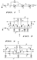
- Burst mode data receiver 10 includes an input stage 12, which in this embodiment is a transimpedance amplifier, having an input terminal 14 constructed to receive non-linear input signals.
- input terminal 14 has a photo diode 16 connected thereto, which diode 16 supplies binary signals to input terminal 14 in response to light impinging thereon.
- Burst mode data receiver 10 further includes an amplifier 18 and a hysteresis stage 20.
- Input stage 12 amplifier 18 and hysteresis stage 20 are all direct coupled with no coupling capacitors required because, as will be more apparent presently, DC inputs have no effect on amplifier 10.
- Signals supplied at input terminal 14 are current signals and output signals from hysteresis stage 20 are amplified voltage replicas of the input current signals.
- FIG. 2 illustrates a schematic diagram of a typical input stage 12.
- Input stage 12 includes a first pair of transistors 25 and 26 connected to provide a differential common emitter stage.
- the common connected emitters of transistors 25 and 26 are connected through a constant current source to a reference potential 27 and the collectors are connected through separate load resistors 28 and 29, respectively, to a power source 30.
- the collectors of transistors 25 and 26 also provide output signals to amplifier 18.
- the base of transistor 25 is connected to the emitter of a transistor 32, which emitter is also connected through a constant current source to the reference potential 27.
- the collector of transistor 32 is connected directly to power source 30 and the base is connected to input terminal 14.
- the base of transistor 26 is connected to the emitter of a transistor 33, which emitter is also connected through a constant current source to the reference potential 27.
- the collector of transistor 33 is connected directly to power source 30 and the base is connected to input terminal 14.
- the bases of transistors 32 and 33 are also separately connected through feedback resistors 35 and 36 to the collectors of transistors 25 and 26, respectively.
- a small capacitor 40 is connected between the base of transistor 26 and ground.
- Capacitor 40 is included to couple the base of transistor 26 to reference 27 and reduce the speed of operation thereof. It will be recognized by those skilled in the art that capacitance 40 could be connected to the emitter of transistor 25, or other components could be utilized at these or other points in the circuit to provide similar results.
- input currents produce a switching action in circuit 12 between transistors 25 and 26, which essentially differentiates the input signal.
- the differentiating action of stage 12 results in output pulses being produced at the collectors of transistors 25 and 26.
- a positive pulse is produced as a result of the positive going front or leading edge of the input current signals and a negative pulse is produced as a result of the negative going back or trailing edge of the input current signals. It will of course be understood by those skilled in the art that the described pulses are simply for purposes of explanation and that a variety of signals indicating the front and back edges of the input signals can be derived.
- the output pulses from input stage 12 are applied to amplifier 18 which in this specific embodiment is a differential amplifier.
- amplifier 18 By utilizing a differential amplifier as amplifier 18, the common mode properties of signals applied thereto are removed and a true differential signal is produced.
- Amplifier 18 is illustrated, for convenience of explanation, as a separate stage in this embodiment, but it should be recognized that it could actually be incorporated into one or both of input stage 12 and hysteresis stage 20. Also.
- amplifier 18 can include as many separate amplifying stages as are required for the specific application. Because the output signals of amplifier 18 are generated from the front and back edges of the input signals, pulse width distortion is virtually eliminated.
- This method and apparatus for producing non-pulse width distorted output signals has the additional advantage of being able to track input signals from less than one microampere to greater than one milliampere, which is a dynamic range of greater than a factor of three (103). Further, the bandwidth of input stage 12 is not critical, linearity is not needed and very slow signals can be tracked, as will be explained in more detail presently.
- hysteresis stage 20 includes a pair of transistors 50 and 51 connected into a differential amplifier configuration with common connected emitters connected through a constant current source to a reference potential 53.
- the collectors of transistors 50 and 51 are connected through individual load resistors 55 and 56, respectively, to a power source 58.
- the collector of transistor 50 is also connected directly to the base of a transistor 60, the collector of which is connected directly to power source 58 and the emitter of which is connected through a constant current source to reference potential 53 and through a resistor 63 to the base of transistor 51.
- the collector of transistor 51 is also connected directly to the base of a transistor 61, the collector of which is connected directly to power source 58 and the emitter of which is connected through a constant current source to reference potential 53 and through a resistor 64 to the base of transistor 50.
- Amplified pulses from the output of amplifier 18 are supplied through a resistor 66 to the base of transistor 50 and through a resistor 67 to the base of transistor 51.
- Output terminals for hysteresis stage 20 are connected to the emitters of transistors 60 and 61, respectively.
- resistors 66 and 67 are equal and the resistances of resistors 63 and 64 are equal.
- Resistors 63 and 64 provide a positive feedback from the output to the base of each transistor 50 and 51 which latches the circuit in one or the other of two output states or logic levels. Resistors 63 and 64 also establish an offset voltage which must be exceeded by input signals before switching between the two output states or logic levels occurs.
- the values of resistors 63 and 64 and resistors 66 and 67 can be changed in various applications to change the offset voltage to suit the application. Because of the latching function of hysteresis stage 20, the output is always latched in one of the possible output states, even when there is no input signal. Thus, it is not necessary to include complicated circuitry for detecting the center point of input signals and centering the output signals around the input signals or providing an input offset voltage or current signal.
- Hysteresis stage 20 provides a number of advantages to burst mode data receiver 10 including the advantage of having a latched output with no input signal. Further, hysteresis stage 20 provides output signals with faster rise and fall times because once hysteresis stage 20 is triggered the output switches states, with the switching time depending only upon the components of hysteresis stage 20. Also, the offset is generally set to be well above noise and other interference signals in the system so that only true data signals will trigger hysteresis stage 20. As previously mentioned, because of the novel hysteresis stage 20 linearity in the previous stages is not a requirement. A clock may be easily incorporated into burst mode data receiver 10, and, especially hysteresis stage 20, to provide clocked output signals, if desired.
- the time/amplitude relationship of several waveforms available at different points in FIG. 1 is represented. Specifically, the input current from photo diode 16 is illustrated in the first line.
- the second line represents typical pulses produced by input stage 12 while the third line represents the pulses amplified by amplifier 18.
- the fourth line represents the regenerated, amplified replicas of the non-linear input signals from line one. Because the output is always latched in one of the logic levels, burst mode data receiver 10 is burst mode ready, that is it is always ready for correct operation on the first bit of data received at input 14. Further, because the output is always latched in one of the logic levels, no sophisticated DC bias restore circuits are required and DC coupling is possible.
- burst mode data receiver 10 has been described as a transimpedance data amplifier which converts a current input to an amplified voltage output, it should be understood that it could be utilized to amplify voltage input signals instead of current input signals. Some modifications to input stage 12 may be required, as for example, resistors 35 and 36 may be removed.
- burst mode data receiver which is simpler to manufacture while maintaining improved sensitivity and burst mode operation. Further, the burst mode data receiver tolerates much higher input capacitances without unduly effecting the sensitivity or dynamic range. Also, the linearity requirements of the burst mode data receiver are greatly relaxed (i.e. bandwidth does not need to be large) and it further incorporates true DC operation, a low quiescent current and a large input current dynamic range. Because of the novel construction clocked outputs can be easily incorporated and the entire burst mode data receiver can be easily integrated on a single semiconductor chip.
Landscapes
- Engineering & Computer Science (AREA)
- Physics & Mathematics (AREA)
- Electromagnetism (AREA)
- Computer Networks & Wireless Communication (AREA)
- Signal Processing (AREA)
- Power Engineering (AREA)
- Amplifiers (AREA)
- Dc Digital Transmission (AREA)
Applications Claiming Priority (2)
| Application Number | Priority Date | Filing Date | Title |
|---|---|---|---|
| US937034 | 1992-08-31 | ||
| US07/937,034 US5394108A (en) | 1992-08-31 | 1992-08-31 | Non-linear burst mode data receiver |
Publications (1)
| Publication Number | Publication Date |
|---|---|
| EP0585557A1 true EP0585557A1 (fr) | 1994-03-09 |
Family
ID=25469390
Family Applications (1)
| Application Number | Title | Priority Date | Filing Date |
|---|---|---|---|
| EP93110586A Withdrawn EP0585557A1 (fr) | 1992-08-31 | 1993-07-02 | Récepteur numérique non-linéaire de données utilisant des rafales |
Country Status (3)
| Country | Link |
|---|---|
| US (1) | US5394108A (fr) |
| EP (1) | EP0585557A1 (fr) |
| JP (1) | JPH06216946A (fr) |
Families Citing this family (2)
| Publication number | Priority date | Publication date | Assignee | Title |
|---|---|---|---|---|
| WO2003009551A2 (fr) * | 2001-07-18 | 2003-01-30 | Vrije Universiteit Brussel (Vub) | Recepteur de signaux numeriques operant au-dela de la frequence 3db |
| KR100601048B1 (ko) * | 2004-04-22 | 2006-07-14 | 한국전자통신연구원 | 버스트 모드 패킷의 수신기 및 그 패킷의 수신 방법 |
Citations (2)
| Publication number | Priority date | Publication date | Assignee | Title |
|---|---|---|---|---|
| EP0430365A1 (fr) * | 1989-11-28 | 1991-06-05 | Philips Composants Et Semiconducteurs | Circuit retardateur à retard réglable |
| EP0444433A2 (fr) * | 1990-03-02 | 1991-09-04 | TEMIC TELEFUNKEN microelectronic GmbH | Circuit pour trigger de Schmitt opto-électronique |
Family Cites Families (15)
| Publication number | Priority date | Publication date | Assignee | Title |
|---|---|---|---|---|
| US3581120A (en) * | 1968-02-28 | 1971-05-25 | Western Union Telegraph Co | Schmitt trigger circuit with variable hysteresis and insensitivity to temperature change |
| US3816760A (en) * | 1971-10-26 | 1974-06-11 | Dahl G Co Inc | Variable level noise barrier circuit responsive to a bipolar input and having variable bipolar hysteresis and having a bipolar output |
| US3843208A (en) * | 1972-07-03 | 1974-10-22 | Texas Instruments Inc | Acceleration and deceleration differentiator circuits for a vehicle skid control braking system |
| JPS5394756A (en) * | 1976-12-28 | 1978-08-19 | Torio Kk | Pulse shaping circuit |
| US4233563A (en) * | 1978-09-06 | 1980-11-11 | Schanbacher William A | Frequency selective hysteresis comparator |
| GB8420651D0 (en) * | 1984-08-14 | 1984-09-19 | British Telecomm | Interface circuit |
| JPS6157118A (ja) * | 1984-08-29 | 1986-03-24 | Toshiba Corp | レベル変換回路 |
| DE3433777A1 (de) * | 1984-09-14 | 1986-03-27 | Robert Bosch Gmbh, 7000 Stuttgart | Impulsformer fuer induktive geber |
| EP0219867B1 (fr) * | 1985-10-23 | 1993-12-29 | Nec Corporation | Circuit logique |
| US4835486A (en) * | 1986-04-28 | 1989-05-30 | Burr-Brown Corporation | Isolation amplifier with precise timing of signals coupled across isolation barrier |
| US4792998A (en) * | 1986-05-23 | 1988-12-20 | Siemens Aktiengesellschaft | Receiver for optical digital signals having different amplitudes |
| US4733107A (en) * | 1986-07-10 | 1988-03-22 | Western Digital Corporation | Low current high precision CMOS schmitt trigger circuit |
| JPH055725Y2 (fr) * | 1987-02-06 | 1993-02-15 | ||
| US4812687A (en) * | 1988-07-13 | 1989-03-14 | International Business Machines Corporation | Dual direction integrating delay circuit |
| US5065054A (en) * | 1990-11-21 | 1991-11-12 | Advanced Micro Devices, Inc. | Input buffer with noise filter for eliminating short-pulse-width noise |
-
1992
- 1992-08-31 US US07/937,034 patent/US5394108A/en not_active Expired - Fee Related
-
1993
- 1993-07-02 EP EP93110586A patent/EP0585557A1/fr not_active Withdrawn
- 1993-08-25 JP JP5230745A patent/JPH06216946A/ja active Pending
Patent Citations (2)
| Publication number | Priority date | Publication date | Assignee | Title |
|---|---|---|---|---|
| EP0430365A1 (fr) * | 1989-11-28 | 1991-06-05 | Philips Composants Et Semiconducteurs | Circuit retardateur à retard réglable |
| EP0444433A2 (fr) * | 1990-03-02 | 1991-09-04 | TEMIC TELEFUNKEN microelectronic GmbH | Circuit pour trigger de Schmitt opto-électronique |
Non-Patent Citations (4)
| Title |
|---|
| JOURNAL OF LIGHTWAVE TECHNOLOGY vol. 8, no. 12, December 1990, NEW YORK US pages 1897 - 1903 OTA 'Burst-Mode Compatible Optical Receiver with a Large Dynamic Range.' * |
| PATENT ABSTRACTS OF JAPAN vol. 12, no. 250 (E-633)14 July 1988 & JP-A-63 037 713 ( KOUDENSHI KOGYO KENKYUSHO ) * |
| PATENT ABSTRACTS OF JAPAN vol. 6, no. 37 (E-97)6 March 1982 & JP-A-56 157 145 ( NEC CORP ) * |
| PATENT ABSTRACTS OF JAPAN vol. 9, no. 244 (E-346)30 September 1985 & JP-A-60 93 856 ( SUMITOMO DENKI KOGYO K.K ) * |
Also Published As
| Publication number | Publication date |
|---|---|
| US5394108A (en) | 1995-02-28 |
| JPH06216946A (ja) | 1994-08-05 |
Similar Documents
| Publication | Publication Date | Title |
|---|---|---|
| JP2625347B2 (ja) | ディジタル受信器の自動オフセット制御回路 | |
| JP2656734B2 (ja) | 光受信回路 | |
| EP0580089A1 (fr) | Récepteur pour signaux optiques, ayant un pré-amplificateur qui corrige le décalage du composant continu et un amplificateur à transimpédance à deux modes de fonctionnement | |
| US5875049A (en) | Amplifier for burst signal and optical receiving circuit | |
| US5182476A (en) | Offset cancellation circuit and method of reducing pulse pairing | |
| US4375037A (en) | Receiving circuit | |
| CN1007031B (zh) | 光接收器 | |
| US4320521A (en) | Data bus transceiver | |
| JP2655130B2 (ja) | ディジタル受信回路 | |
| US4994692A (en) | Quantizer system | |
| JPH05136635A (ja) | 信号受信装置 | |
| US5394108A (en) | Non-linear burst mode data receiver | |
| US4817208A (en) | Fiber optic receiver | |
| US7049856B2 (en) | High speed peak amplitude comparator | |
| EP0865683A1 (fr) | Recepteur de donnees en serie fonctionnant a des debits de plusieurs gigabits par seconde | |
| US5373388A (en) | AC coupled fiber optic receiver with DC coupled characteristics | |
| US6194965B1 (en) | Differential signal detection circuit | |
| JPH09289495A (ja) | バースト信号用増幅器および光受信回路 | |
| US4142110A (en) | Circuit to eliminate DC bias | |
| US4093876A (en) | Baseline restorer circuit | |
| US4795919A (en) | Zero signal state detecting circuit | |
| US3911363A (en) | Delta modulation circuitry with automatic squelch and gain control | |
| WO1999040574A2 (fr) | Dispositif de lecture d'informations sur un support d'enregistrement magnetique | |
| JP2531922B2 (ja) | 単極性符号・双極性符号変換回路 | |
| JP3266769B2 (ja) | 受光増幅回路 |
Legal Events
| Date | Code | Title | Description |
|---|---|---|---|
| PUAI | Public reference made under article 153(3) epc to a published international application that has entered the european phase |
Free format text: ORIGINAL CODE: 0009012 |
|
| AK | Designated contracting states |
Kind code of ref document: A1 Designated state(s): DE FR GB |
|
| 17P | Request for examination filed |
Effective date: 19940909 |
|
| 17Q | First examination report despatched |
Effective date: 19970909 |
|
| STAA | Information on the status of an ep patent application or granted ep patent |
Free format text: STATUS: THE APPLICATION IS DEEMED TO BE WITHDRAWN |
|
| 18D | Application deemed to be withdrawn |
Effective date: 19980120 |