EP0445038A1 - Bildabtastungsvorrichtung, bestehend aus einer Matrix statischer Ladungssensoren - Google Patents
Bildabtastungsvorrichtung, bestehend aus einer Matrix statischer Ladungssensoren Download PDFInfo
- Publication number
- EP0445038A1 EP0445038A1 EP91400555A EP91400555A EP0445038A1 EP 0445038 A1 EP0445038 A1 EP 0445038A1 EP 91400555 A EP91400555 A EP 91400555A EP 91400555 A EP91400555 A EP 91400555A EP 0445038 A1 EP0445038 A1 EP 0445038A1
- Authority
- EP
- European Patent Office
- Prior art keywords
- matrix
- sensors
- lines
- charges
- transfer
- Prior art date
- Legal status (The legal status is an assumption and is not a legal conclusion. Google has not performed a legal analysis and makes no representation as to the accuracy of the status listed.)
- Granted
Links
Images

Classifications
-
- H—ELECTRICITY
- H04—ELECTRIC COMMUNICATION TECHNIQUE
- H04N—PICTORIAL COMMUNICATION, e.g. TELEVISION
- H04N25/00—Circuitry of solid-state image sensors [SSIS]; Control thereof
- H04N25/50—Control of the SSIS exposure
- H04N25/53—Control of the integration time
-
- H—ELECTRICITY
- H04—ELECTRIC COMMUNICATION TECHNIQUE
- H04N—PICTORIAL COMMUNICATION, e.g. TELEVISION
- H04N23/00—Cameras or camera modules comprising electronic image sensors; Control thereof
- H04N23/20—Cameras or camera modules comprising electronic image sensors; Control thereof for generating image signals from infrared radiation only
-
- H—ELECTRICITY
- H04—ELECTRIC COMMUNICATION TECHNIQUE
- H04N—PICTORIAL COMMUNICATION, e.g. TELEVISION
- H04N25/00—Circuitry of solid-state image sensors [SSIS]; Control thereof
- H04N25/70—SSIS architectures; Circuits associated therewith
- H04N25/71—Charge-coupled device [CCD] sensors; Charge-transfer registers specially adapted for CCD sensors
- H04N25/711—Time delay and integration [TDI] registers; TDI shift registers
Definitions
- the invention relates to imaging devices of the type comprising a camera having a matrix of charge accumulation sensors, in particular of so-called charge coupled sensors, and means making it possible to transfer the charges accumulated by the sensors, in a short time. relative to the accumulation time, either entirely in a memory comprising a number of memory points equal to that of the sensors, or from each of the lines of sensors in a respective memory, then emptying the memories via a shift register receiving all the content of a column at once.
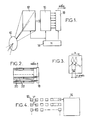
- FIG. 1 shows the principle of known imaging devices of the type defined above.
- the device shown in FIG. 1 comprises an optic 10 for forming the image of a scene on a matrix of sensors 12, distributed in rows and columns.
- a clock 14 causes the transfer of the charges accumulated on all the sensors to a memory 16, in the direction of the lines. Detection and accumulation of charges can then resume immediately on the matrix 12.
- the charges contained in each column in turn are transferred to a shift register 18 whose serial output constitutes the video output of the device.
- FIG. 2 shows a device using instead a line-to-line transfer matrix.
- Each line of sensors 20 is associated with a line of memory points 22, where the accumulation of charges takes place.
- These loads are transferred, one column at a time, to an output shift register 18 similar to that of FIG. 1.
- cameras comprising a sensitive member constituted by several lines of sensors placed parallel to each other, a scanning mirror of the sensitive member transversely to the lines and means for shifting the charges from one line to the next to a cadence synchronized with the displacement of the image of a section of the scene on the matrix.
- the invention aims to provide a scanning imaging device comprising a matrix of sensors, requiring only simple modifications of the control means of a matrix of conventional constitution, without loss of resolution or sensitivity; an additional result which the invention aims to achieve consists in enabling wide field or even panoramic surveillance with a camera having a narrow field.
- the invention proposes in particular a device of the type defined above, characterized in that it comprises means for scanning the scene observed in the direction of the lines (direction in which the field is weakest in general ), means for transferring the charges in the direction of the lines in synchronism with the scanning for a duration equal to a predetermined integration time, and for transferring all charges to the register in a short time compared to the integration time.
- Figures 1 and 2 already mentioned, show the construction of the principle of a fixed imaging device with a matrix of sensors.
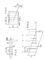
- Figures 4 and 5 show the evolution of the loads during the transfer, respectively in the case of a frame transfer device and a line to line transfer device.
- FIG. 6 schematically shows the displacement of a scene in the field of vision of the matrix as a function of time, in the case of an overlap of order equal to 3.
- Figure 7 shows the partial movement of successive images during scanning.
- FIG. 8 is a block diagram of timing circuits usable for implementing the invention.
- the device comprises scanning means, such as a mirror, causing the image of the scene to scroll at a speed Vs in the direction indicated by the arrow x in FIG. 3, this is ie in the direction of the lines (direction of charge transfer to the shift register 18).
- Vs the speed in the direction indicated by the arrow x in FIG. 3
- this displacement corresponds to n detectors.
- the charges must be moved in the direction of the lines, at the same speed Vs as the speed of movement of the image.
- the sensor matrix 12 In the case of a frame transfer matrix (FIG. 4), where the entire image is transferred completely and quickly to the memory area 16 in a time t d , the sensor matrix 12 must be controlled so to cause successive transfers of amplitude charges c corresponding to the distance between successive sensors of the same line, with a period t i / n, before the complete transfer.
- the integration time t i must in practice be a few tens of ms and it precedes the complete transfer of frame, the duration t d is much lower.
- This recovery order is not the only possible one. In practice it can be between 2 and 10. Due to the transfer during t i , the first image available at t0 + t i corresponds to Nn pixels only; a pixel at the head of this available image will still be available at t0 + t i + T and t0 + t i + 2T, while a pixel at the bottom at time t0 + t i has already been available twice.
- the spatial resolution is around 0.5 milliradians, that is to say 2 minutes.
- the device can also be used to make a panoramic surveillance, by turning it at constant speed: the duration of a revolution is then about 2.6 seconds.
- the device makes it possible to carry out an infrared or visible watch with a conventional charge-accumulation sensor camera, with a tolerable loss of field at the top of each displayed band. But there is no loss of angular field in the direction transverse to the scan.
- FIG. 8 shows a possible constitution of the circuits supplying the different timing signals from the signal of a main clock oscillator 14, at a frequency of 80 MHz.
- the additional circuits required are limited to two generators 24 and 26, the outputs of which are connected to circuits 28 and 30 for driving the sensor array.
Landscapes
- Engineering & Computer Science (AREA)
- Multimedia (AREA)
- Signal Processing (AREA)
- Transforming Light Signals Into Electric Signals (AREA)
Applications Claiming Priority (2)
| Application Number | Priority Date | Filing Date | Title |
|---|---|---|---|
| FR9002586A FR2659182B1 (fr) | 1990-03-01 | 1990-03-01 | Dispositif d'imagerie a balayage, comportant une matrice de capteurs a accumulation de charges. |
| FR9002586 | 1990-03-01 |
Publications (2)
| Publication Number | Publication Date |
|---|---|
| EP0445038A1 true EP0445038A1 (de) | 1991-09-04 |
| EP0445038B1 EP0445038B1 (de) | 1995-04-12 |
Family
ID=9394283
Family Applications (1)
| Application Number | Title | Priority Date | Filing Date |
|---|---|---|---|
| EP91400555A Expired - Lifetime EP0445038B1 (de) | 1990-03-01 | 1991-02-28 | Bildabtastungsvorrichtung, bestehend aus einer Matrix statischer Ladungssensoren |
Country Status (3)
| Country | Link |
|---|---|
| EP (1) | EP0445038B1 (de) |
| DE (1) | DE69108759T2 (de) |
| FR (1) | FR2659182B1 (de) |
Cited By (3)
| Publication number | Priority date | Publication date | Assignee | Title |
|---|---|---|---|---|
| WO1992010059A1 (en) * | 1990-11-28 | 1992-06-11 | Recon/Optical, Inc. | Electro-optical imaging array with motion compensation |
| US5692062A (en) * | 1994-10-03 | 1997-11-25 | Recon/Optical, Inc. | Electro-optical imaging array with profiled foward motion compensation |
| CN106959509A (zh) * | 2017-03-01 | 2017-07-18 | 北京理工大学 | 一种凝视型周视等作用距离红外成像系统设计方法 |
Citations (1)
| Publication number | Priority date | Publication date | Assignee | Title |
|---|---|---|---|---|
| EP0223119A1 (de) * | 1985-11-04 | 1987-05-27 | Compagnie des Montres Longines, Francillon S.A. | Rennsportzeitmessgerät |
-
1990
- 1990-03-01 FR FR9002586A patent/FR2659182B1/fr not_active Expired - Fee Related
-
1991
- 1991-02-28 DE DE69108759T patent/DE69108759T2/de not_active Expired - Fee Related
- 1991-02-28 EP EP91400555A patent/EP0445038B1/de not_active Expired - Lifetime
Patent Citations (1)
| Publication number | Priority date | Publication date | Assignee | Title |
|---|---|---|---|---|
| EP0223119A1 (de) * | 1985-11-04 | 1987-05-27 | Compagnie des Montres Longines, Francillon S.A. | Rennsportzeitmessgerät |
Cited By (3)
| Publication number | Priority date | Publication date | Assignee | Title |
|---|---|---|---|---|
| WO1992010059A1 (en) * | 1990-11-28 | 1992-06-11 | Recon/Optical, Inc. | Electro-optical imaging array with motion compensation |
| US5692062A (en) * | 1994-10-03 | 1997-11-25 | Recon/Optical, Inc. | Electro-optical imaging array with profiled foward motion compensation |
| CN106959509A (zh) * | 2017-03-01 | 2017-07-18 | 北京理工大学 | 一种凝视型周视等作用距离红外成像系统设计方法 |
Also Published As
| Publication number | Publication date |
|---|---|
| FR2659182B1 (fr) | 1992-06-19 |
| FR2659182A1 (fr) | 1991-09-06 |
| DE69108759T2 (de) | 1995-12-07 |
| EP0445038B1 (de) | 1995-04-12 |
| DE69108759D1 (de) | 1995-05-18 |
Similar Documents
| Publication | Publication Date | Title |
|---|---|---|
| EP0178954B1 (de) | Verfahren und Einrichtung zur Abtastung eines Fensters im Bildbereich einer bildorganisierten Ladungsübertragungsanordnung | |
| EP0265302B1 (de) | Schnelle Videobildaufnahme mit einem optischen matrixförmigen Ladungsübertragungssensor | |
| EP2056590B1 (de) | Verfahren und Vorrichtung zum Pixelsauslesen aus einer bidimensionalen Matrix | |
| EP0254634B1 (de) | Verfahren und Vorrichtung zum optischen Abstandsmessen | |
| FR2502875A1 (fr) | Procede et dispositif de cadrage et de stabilisation d'image de camera electro-optique | |
| FR2676284A1 (fr) | Procede de detection d'obstacles presents devant un vehicule automobile et dispositif pour la mise en óoeuvre d'un tel procede. | |
| FR2508748A1 (fr) | Systeme et procede pour convertir un signal video non entrelace en un signal video entrelace | |
| EP0575220B1 (de) | Multistandard-Beobachtungskamera und Überwachungssystem damit | |
| JP4259749B2 (ja) | 高速プロファイリングのためのエンハンスドフレーム転送周波数で駆動したライン間転送ccd | |
| FR2696843A1 (fr) | Appareil de prise de vues à distance, à haute résolution, pour porteur aérien. | |
| WO1992003016A2 (fr) | Camera panoramique du type a transfert de charges dans un systeme de veille | |
| FR2608341A1 (fr) | Appareil capteur d'image a l'etat solide du type a dispositif a couplage de charge et procede de commande d'un tel appareil | |
| EP0738074A1 (de) | Detektionsverfahren mit verteilten Integrations- und Ausleseperioden für eine Abtastungskamera, und entsprechende Detektoranordnung | |
| EP0222641B1 (de) | Einrichtungen für elektronische Überblendung | |
| EP0445038B1 (de) | Bildabtastungsvorrichtung, bestehend aus einer Matrix statischer Ladungssensoren | |
| FR2667182A1 (fr) | Capteur de camera et procede de balayage d'image. | |
| EP0452188B1 (de) | Abbildungs- und Überwachungsvorrichtung mit Matrixsensor | |
| US5297762A (en) | Optical navigation sensor with single two-dimensional CCD | |
| EP0657019B1 (de) | Hochauflosendes weitwinkel-abbildungsgerat fur luftfahrzeug | |
| EP0235002B1 (de) | Optoelektronischer Ladungübertragungssensor | |
| CA1266523A (fr) | Senseur opto-electronique multichamp a transfert de charges | |
| FR2588709A1 (fr) | Systeme de grossissement d'une partie d'une image dans les dispositifs de prise de vues video notamment a senseur a transfert de charges | |
| EP0516543B1 (de) | Laufende, optoelektronische Bildaufnahmevorrichtung | |
| FR2580865A1 (fr) | Appareil d'imagerie thermique afocal | |
| EP1112653B1 (de) | Kinevideokamera |
Legal Events
| Date | Code | Title | Description |
|---|---|---|---|
| PUAI | Public reference made under article 153(3) epc to a published international application that has entered the european phase |
Free format text: ORIGINAL CODE: 0009012 |
|
| AK | Designated contracting states |
Kind code of ref document: A1 Designated state(s): DE GB IT |
|
| 17P | Request for examination filed |
Effective date: 19911209 |
|
| 17Q | First examination report despatched |
Effective date: 19940315 |
|
| GRAA | (expected) grant |
Free format text: ORIGINAL CODE: 0009210 |
|
| AK | Designated contracting states |
Kind code of ref document: B1 Designated state(s): DE GB IT |
|
| GBT | Gb: translation of ep patent filed (gb section 77(6)(a)/1977) |
Effective date: 19950410 |
|
| ITF | It: translation for a ep patent filed | ||
| REF | Corresponds to: |
Ref document number: 69108759 Country of ref document: DE Date of ref document: 19950518 |
|
| PLBE | No opposition filed within time limit |
Free format text: ORIGINAL CODE: 0009261 |
|
| STAA | Information on the status of an ep patent application or granted ep patent |
Free format text: STATUS: NO OPPOSITION FILED WITHIN TIME LIMIT |
|
| 26N | No opposition filed | ||
| REG | Reference to a national code |
Ref country code: GB Ref legal event code: IF02 |
|
| PGFP | Annual fee paid to national office [announced via postgrant information from national office to epo] |
Ref country code: DE Payment date: 20060203 Year of fee payment: 16 |
|
| PGFP | Annual fee paid to national office [announced via postgrant information from national office to epo] |
Ref country code: GB Payment date: 20060207 Year of fee payment: 16 |
|
| PGFP | Annual fee paid to national office [announced via postgrant information from national office to epo] |
Ref country code: IT Payment date: 20060228 Year of fee payment: 16 |
|
| GBPC | Gb: european patent ceased through non-payment of renewal fee |
Effective date: 20070228 |
|
| PG25 | Lapsed in a contracting state [announced via postgrant information from national office to epo] |
Ref country code: DE Free format text: LAPSE BECAUSE OF NON-PAYMENT OF DUE FEES Effective date: 20070901 |
|
| PG25 | Lapsed in a contracting state [announced via postgrant information from national office to epo] |
Ref country code: GB Free format text: LAPSE BECAUSE OF NON-PAYMENT OF DUE FEES Effective date: 20070228 |
|
| PG25 | Lapsed in a contracting state [announced via postgrant information from national office to epo] |
Ref country code: IT Free format text: LAPSE BECAUSE OF NON-PAYMENT OF DUE FEES Effective date: 20070228 |