EP0445527A2 - Composante optique de guide d'onde et m˩thode de fabrication d'une composante optique de guide d'onde - Google Patents
Composante optique de guide d'onde et m˩thode de fabrication d'une composante optique de guide d'onde Download PDFInfo
- Publication number
- EP0445527A2 EP0445527A2 EP19910101404 EP91101404A EP0445527A2 EP 0445527 A2 EP0445527 A2 EP 0445527A2 EP 19910101404 EP19910101404 EP 19910101404 EP 91101404 A EP91101404 A EP 91101404A EP 0445527 A2 EP0445527 A2 EP 0445527A2
- Authority
- EP
- European Patent Office
- Prior art keywords
- channel
- polymer
- protective layer
- optical waveguide
- optical
- Prior art date
- Legal status (The legal status is an assumption and is not a legal conclusion. Google has not performed a legal analysis and makes no representation as to the accuracy of the status listed.)
- Granted
Links
- 230000003287 optical effect Effects 0.000 title claims abstract description 72
- 238000004519 manufacturing process Methods 0.000 title claims abstract description 8
- 229920000642 polymer Polymers 0.000 claims abstract description 51
- 239000011241 protective layer Substances 0.000 claims abstract description 35
- 239000011521 glass Substances 0.000 claims abstract description 32
- 238000000034 method Methods 0.000 claims abstract description 31
- 239000000758 substrate Substances 0.000 claims abstract description 29
- KRHYYFGTRYWZRS-UHFFFAOYSA-N Fluorane Chemical compound F KRHYYFGTRYWZRS-UHFFFAOYSA-N 0.000 claims abstract description 22
- 239000010410 layer Substances 0.000 claims description 28
- 229910052751 metal Inorganic materials 0.000 claims description 15
- 239000002184 metal Substances 0.000 claims description 15
- 230000005684 electric field Effects 0.000 claims description 6
- 238000005530 etching Methods 0.000 claims description 6
- PCHJSUWPFVWCPO-UHFFFAOYSA-N gold Chemical compound [Au] PCHJSUWPFVWCPO-UHFFFAOYSA-N 0.000 claims description 6
- 229910052737 gold Inorganic materials 0.000 claims description 6
- 239000010931 gold Substances 0.000 claims description 6
- 229910052715 tantalum Inorganic materials 0.000 claims description 6
- GUVRBAGPIYLISA-UHFFFAOYSA-N tantalum atom Chemical compound [Ta] GUVRBAGPIYLISA-UHFFFAOYSA-N 0.000 claims description 6
- 230000010287 polarization Effects 0.000 claims description 5
- 239000004642 Polyimide Substances 0.000 claims description 4
- 230000035515 penetration Effects 0.000 claims description 4
- 229920001721 polyimide Polymers 0.000 claims description 4
- 239000007788 liquid Substances 0.000 claims description 3
- 230000003647 oxidation Effects 0.000 claims description 3
- 238000007254 oxidation reaction Methods 0.000 claims description 3
- 239000000178 monomer Substances 0.000 claims description 2
- BPUBBGLMJRNUCC-UHFFFAOYSA-N oxygen(2-);tantalum(5+) Chemical compound [O-2].[O-2].[O-2].[O-2].[O-2].[Ta+5].[Ta+5] BPUBBGLMJRNUCC-UHFFFAOYSA-N 0.000 claims description 2
- 230000005855 radiation Effects 0.000 claims description 2
- 238000007740 vapor deposition Methods 0.000 claims 1
- 239000003365 glass fiber Substances 0.000 abstract description 5
- 230000005540 biological transmission Effects 0.000 abstract description 4
- 230000008878 coupling Effects 0.000 description 5
- 238000010168 coupling process Methods 0.000 description 5
- 238000005859 coupling reaction Methods 0.000 description 5
- 229920002120 photoresistant polymer Polymers 0.000 description 4
- 229920003229 poly(methyl methacrylate) Polymers 0.000 description 3
- 238000006116 polymerization reaction Methods 0.000 description 3
- 239000004926 polymethyl methacrylate Substances 0.000 description 3
- 208000026817 47,XYY syndrome Diseases 0.000 description 2
- 230000001680 brushing effect Effects 0.000 description 2
- 238000001035 drying Methods 0.000 description 2
- 239000000463 material Substances 0.000 description 2
- 238000001465 metallisation Methods 0.000 description 2
- 239000010453 quartz Substances 0.000 description 2
- VYPSYNLAJGMNEJ-UHFFFAOYSA-N silicon dioxide Inorganic materials O=[Si]=O VYPSYNLAJGMNEJ-UHFFFAOYSA-N 0.000 description 2
- 238000004528 spin coating Methods 0.000 description 2
- PBCFLUZVCVVTBY-UHFFFAOYSA-N tantalum pentoxide Inorganic materials O=[Ta](=O)O[Ta](=O)=O PBCFLUZVCVVTBY-UHFFFAOYSA-N 0.000 description 2
- 230000006978 adaptation Effects 0.000 description 1
- 239000003795 chemical substances by application Substances 0.000 description 1
- 238000013016 damping Methods 0.000 description 1
- 238000003780 insertion Methods 0.000 description 1
- 230000037431 insertion Effects 0.000 description 1
- YTCQFLFGFXZUSN-BAQGIRSFSA-N microline Chemical compound OC12OC3(C)COC2(O)C(C(/Cl)=C/C)=CC(=O)C21C3C2 YTCQFLFGFXZUSN-BAQGIRSFSA-N 0.000 description 1
- 230000000149 penetrating effect Effects 0.000 description 1
- 239000004033 plastic Substances 0.000 description 1
- 229920003023 plastic Polymers 0.000 description 1
- 238000003825 pressing Methods 0.000 description 1
- 230000001681 protective effect Effects 0.000 description 1
- 239000002904 solvent Substances 0.000 description 1
- 238000003860 storage Methods 0.000 description 1
- 229910001936 tantalum oxide Inorganic materials 0.000 description 1
- 238000010345 tape casting Methods 0.000 description 1
- 230000002123 temporal effect Effects 0.000 description 1
- 239000002966 varnish Substances 0.000 description 1
Images
Classifications
-
- G—PHYSICS
- G02—OPTICS
- G02F—OPTICAL DEVICES OR ARRANGEMENTS FOR THE CONTROL OF LIGHT BY MODIFICATION OF THE OPTICAL PROPERTIES OF THE MEDIA OF THE ELEMENTS INVOLVED THEREIN; NON-LINEAR OPTICS; FREQUENCY-CHANGING OF LIGHT; OPTICAL LOGIC ELEMENTS; OPTICAL ANALOGUE/DIGITAL CONVERTERS
- G02F1/00—Devices or arrangements for the control of the intensity, colour, phase, polarisation or direction of light arriving from an independent light source, e.g. switching, gating or modulating; Non-linear optics
- G02F1/01—Devices or arrangements for the control of the intensity, colour, phase, polarisation or direction of light arriving from an independent light source, e.g. switching, gating or modulating; Non-linear optics for the control of the intensity, phase, polarisation or colour
- G02F1/061—Devices or arrangements for the control of the intensity, colour, phase, polarisation or direction of light arriving from an independent light source, e.g. switching, gating or modulating; Non-linear optics for the control of the intensity, phase, polarisation or colour based on electro-optical organic material
- G02F1/065—Devices or arrangements for the control of the intensity, colour, phase, polarisation or direction of light arriving from an independent light source, e.g. switching, gating or modulating; Non-linear optics for the control of the intensity, phase, polarisation or colour based on electro-optical organic material in an optical waveguide structure
-
- G—PHYSICS
- G02—OPTICS
- G02B—OPTICAL ELEMENTS, SYSTEMS OR APPARATUS
- G02B6/00—Light guides; Structural details of arrangements comprising light guides and other optical elements, e.g. couplings
- G02B6/10—Light guides; Structural details of arrangements comprising light guides and other optical elements, e.g. couplings of the optical waveguide type
- G02B6/12—Light guides; Structural details of arrangements comprising light guides and other optical elements, e.g. couplings of the optical waveguide type of the integrated circuit kind
- G02B6/13—Integrated optical circuits characterised by the manufacturing method
- G02B6/136—Integrated optical circuits characterised by the manufacturing method by etching
Definitions
- the present invention relates to an optical waveguide component according to the preamble of claim 1 and to a method for producing an optical waveguide component according to the preamble of claim 7.
- planar structures are known in which an optical polymer is applied in a very thin layer to a glass substrate and is then photolithographically structured in accordance with the desired waveguide or waveguides.
- the object of the present invention is to create an optical waveguide component of the type mentioned at the outset, in which the cross-sectional geometry of the optical waveguides that of the transmission glass fibers used for the optical waveguide comes considerably closer, so that coupling losses are significantly reduced and a corresponding adjustment is achieved.
- a method for producing an optical waveguide component is to be created which enables such a cross-sectional geometry adjustment and which is relatively inexpensive and ensures good optical results of the optical waveguides.
- the features specified in claim 1 are provided in an optical waveguide component of the type mentioned and the features specified in claim 7 in a method for producing an optical waveguide component of the type mentioned.
- the measures according to the invention make it possible to create optical waveguide components in a relatively simple manner, in which the optical waveguide (s) have a cross section, the length and width of which are approximated to one another in certain wide ranges, at least to the extent that it is optical with the cross-sectional geometry of a glass fiber is comparable '. If we are talking about at least one optical waveguide component, this can be a simple transmission component but also act on coupling components, branching components and the like.
- the advantage here is that the coupling of light from a glass fiber transmission link into the optical waveguide component can proceed without problems due to the optical approximation of the cross sections, so that the high coupling and decoupling losses that have occurred to date are significantly reduced.
- light waves of any shape can be applied to or embedded in the glass substrate, ie not only straight, but also curved, Y-shaped, double-Y-shaped and the like.
- the geometry adaptation can be optimized in a simple manner by using the features of claim 8.
- NLO non-linear optical
- the effective penetration of the electric field through the quartz of the glass substrate is reduced if it is assumed that the electrodes in question for producing the electric field are attached to the opposite outer surfaces of the glass substrate. This is not least because the electrical conductivity of the NLO polymer is greater than that of the quartz of the glass substrate.
- the features specified in claim 2 and / or 3 or in claim 9 are provided. As a result, the electrodes are brought directly to the NLO polymer, which is already shaped to the final geometry of the optical waveguide.
- the polymerization of the NLO polymer and its penetration into the etched channel is advantageously carried out using the features of one or more of claims 10 to 13.
- this can be carried out by spin coating or brushing on , Doctor blade or the like.
- the protective layer to be applied to the glass substrate which should be resistant to the hydrofluoric acid for etching the glass substrate, and for reaching the relevant line structure of the optical waveguides to be incorporated, there are numerous possibilities, such as those in the optical waveguide component by the features of claims 4 and 5 and Method for producing an optical waveguide component by which the features of claims 14 to 16 are defined. If a tantalum layer is used, a Ta2O5 layer is achieved by the thermal oxidation process. It is advantageous in all cases that the structures can be reached photolithographically.
- This protective layer is also expedient because when the channel is etched out using buffered or non-buffered hydrofluoric acid in the glass substrate, a channel widening with a trapezoidal boundary line is created below the edges of the protective layer, so that subsequent insertion of the electrode layer from the open side of the channel is prevented. that the side walls of the channel are also covered by the metallic electrode.
- optical waveguide components of almost any type, such as, for example, couplers, branching devices, polarization regulators, optical isolators and the like.
- Optical waveguides can be used in any of the optical waveguide components Shapes can be realized, that is, rectilinear, curved or curved, Y-shaped, double-Y-shaped and the like.
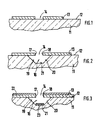
- a glass substrate 11 is used as the basis for producing an optical waveguide component, the base area of which corresponds to that of the waveguide component to be produced.
- a surface 12 of the glass substrate 11 is covered with a protective layer 13.
- the protective layer 13 can be made of tantalum, for example, but also made of gold or a plastic, namely polyimide. These materials which can be used for the protective layer 13 can be subjected to a photolithographic process by means of which fine line structures are etched into the protective layer 13 with the aid of a suitable etching agent, specifically at the points at which optical waveguides are to be provided.
- 1 shows such a micro line or micro gap 14 in the protective layer 13.
- the micro-gap 14 has a width of 7 ⁇ m, the length being arbitrary, depending on what is to be achieved with the optical waveguide or the optical waveguide arrangement on or in the waveguide component.
- the tantalum layer is subjected to a thermal oxidation process which takes place in air at about 400 ° C. for several hours and with which a protective Ta2O5 layer is reached.
- the protective layer 14 of tantalum oxide, gold or polyimide applied in this way is resistant to buffered or unbuffered hydrofluoric acid, which is used as an etchant for the glass substrate 11.
- Hydrofluoric acid is now brought onto the surface 12 of the glass substrate 11 via the micro-gap 14, so that the channel 16 shown in FIG. 2 is reached. Since the hydrofluoric acid penetrating through the micro-gap 14 also spreads under the longitudinal edges 17 and 18 of the protective layer 13 that delimit the micro-gap 14 during the etching of the glass substrate 11, a trapezoidal boundary surface 19 results due to the temporal effect of the hydrofluoric acid on the glass substrate 11 depending on the penetration depth , 20 of the channel 16.
- the glass substrate 11 is exposed to the buffered or non-buffered hydrofluoric acid until the channel 16 has reached a depth of approximately 5 to 7 ⁇ m, that is to say a depth which is approximately the width of the microgap 14 or the Corresponds to the width of the channel base 21.
- This achieves a cross-sectional geometry of the channel 16 in which the two dimensions with respect to depth or height and width are approximated to one another on average, at least not by one Multiple apart.
- the cross-sectional geometry of the channel 16 or the inclination of its flanks 19.20 can be influenced within certain limits depending on the type and duration of action of the hydrofluoric acid.
- the channel 16 could now be filled with the relevant polymer, which would be followed either by a polymerisation process for the optical polymer or a drying process.
- NLO non-linear optical
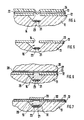
- a metal layer 22 is first applied, for example and preferably vapor-deposited, to the protective layer 13 either over the entire area or only in the area of the respective microgaps 14, as shown in FIG. 3.
- gold can be used for the metal layer 22.
- the metal for example gold, reaches the bottom 21 of the channel 16 through the micro-gap or 14.
- the longitudinal edges 17 and 18 of the protective layer 13 have the trapezoidal boundary surfaces or project beyond flanks 19 and 20 of channel 16, it is achieved that during this metallization process the metal entering channel 16 does not reach flanks 19 and 20, but merely forms an electrode 23 on channel base 21 and there.
- a glass plate 26 with its metallized side 27 is placed over the entire surface of the protective layer 13 according to FIG. 6, it goes without saying that the metal layer 27 on the glass plate 26 also only in that of the electrode or electrodes 23 on the channel base 21 opposite area or areas can be provided.
- the channel is closed on all sides and thus formed into a capillary.
- the channel (s) 16, including the micro-gap (s) 14, are now filled with liquid NLO polymer 29, which can be done, for example, by pressing into a storage recess with the aid of a tip or from an open channel end.
- a monomer or prepolymer can be used as the NLO polymer 29.
- the NLO polymer is then polymerized thermally or with UV radiation. It is also possible to use a dissolved NLO polymer which, after being introduced into the channel 16, must then be freed from solvent, that is to say dried, which should, however, expediently take place with the glass plate 26 removed.
- the NLO polymer 29 must be polarized in order to give it an optical preferred direction and thus one give the corresponding refractive index.
- the polarization of the NLO polymer takes place by applying a large electric field between the electrode 23 on the channel base 21 and the metal layer 27 on the glass plate 26 lying on it. The light wave widened (section) is thus produced.
- the finished optical waveguide component results, which, depending on the type and type of the waveguide component, can be equipped with further electrodes. Possibly.
- a dielectric intermediate layer 28 can be arranged between counter electrode 27 and protective layer or NLO polymer.
- a dielectric intermediate layer 31 is first applied to the electrode 23 on the channel base 21 following the method step according to FIG. 5.
- This dielectric intermediate layer 31 can consist, for example, of PMMA (polymethyl methacrylate).
- the NLO polymer is introduced into the channel 16 in the liquid state, which can be done, for example, by spin coating, brushing, knife coating or the like.
- a polymerization process or a drying process follows.
- An upper dielectric intermediate layer 32 is applied over the microgaps 14 and can also be made of PMMA, for example.
- a counterelectrode 33 is then placed on the upper dielectric intermediate layer 32 either over the entire surface or in the region of the channel 16, ie opposite the electrode 23.
- the upper and lower dielectric intermediate layers 31, 32 serve to optically separate the NLO polymer from the metal electrodes 23 and 33.
Landscapes
- Physics & Mathematics (AREA)
- Nonlinear Science (AREA)
- General Physics & Mathematics (AREA)
- Optics & Photonics (AREA)
- Engineering & Computer Science (AREA)
- Microelectronics & Electronic Packaging (AREA)
- Optical Integrated Circuits (AREA)
- Glass Compositions (AREA)
- Optical Couplings Of Light Guides (AREA)
Applications Claiming Priority (2)
| Application Number | Priority Date | Filing Date | Title |
|---|---|---|---|
| DE4006863 | 1990-03-05 | ||
| DE4006863A DE4006863A1 (de) | 1990-03-05 | 1990-03-05 | Optisches wellenleiterbauelement und verfahren zum herstellen eines optischen wellenleiterbauelementes |
Publications (3)
| Publication Number | Publication Date |
|---|---|
| EP0445527A2 true EP0445527A2 (fr) | 1991-09-11 |
| EP0445527A3 EP0445527A3 (en) | 1992-04-29 |
| EP0445527B1 EP0445527B1 (fr) | 1994-10-12 |
Family
ID=6401451
Family Applications (1)
| Application Number | Title | Priority Date | Filing Date |
|---|---|---|---|
| EP91101404A Expired - Lifetime EP0445527B1 (fr) | 1990-03-05 | 1991-02-02 | Composante optique de guide d'onde et méthode de fabrication d'une composante optique de guide d'onde |
Country Status (4)
| Country | Link |
|---|---|
| EP (1) | EP0445527B1 (fr) |
| AT (1) | ATE112859T1 (fr) |
| DE (2) | DE4006863A1 (fr) |
| ES (1) | ES2065558T3 (fr) |
Cited By (11)
| Publication number | Priority date | Publication date | Assignee | Title |
|---|---|---|---|---|
| EP0551118A1 (fr) * | 1992-01-10 | 1993-07-14 | INSTITUT FÜR MIKROTECHNIK MAINZ GmbH | Procédé de fabrication d'éléments microoptiques non-linéaires |
| EP0551119A1 (fr) * | 1992-01-10 | 1993-07-14 | INSTITUT FÜR MIKROTECHNIK MAINZ GmbH | Procédé de fabrication d'éléments microoptiques non-linéaires |
| EP0559040A1 (fr) * | 1992-02-29 | 1993-09-08 | Alcatel SEL Aktiengesellschaft | Procédé de fabrication de composants optoélectroniques |
| US5970186A (en) * | 1997-03-11 | 1999-10-19 | Lightwave Microsystems Corporation | Hybrid digital electro-optic switch |
| US6022671A (en) * | 1997-03-11 | 2000-02-08 | Lightwave Microsystems Corporation | Method of making optical interconnects with hybrid construction |
| US6144779A (en) * | 1997-03-11 | 2000-11-07 | Lightwave Microsystems Corporation | Optical interconnects with hybrid construction |
| US6311004B1 (en) | 1998-11-10 | 2001-10-30 | Lightwave Microsystems | Photonic devices comprising thermo-optic polymer |
| WO2002067019A3 (fr) * | 2001-02-20 | 2002-11-07 | Univ Ramot | Structure de guide d'ondes polymere sur substrat et procede de production correspondant |
| US20130279845A1 (en) * | 2011-12-21 | 2013-10-24 | Mauro J. Kobrinsky | Fabrication of planar light-wave circuits (plcs) for optical i/o |
| FR3057677A1 (fr) * | 2016-10-13 | 2018-04-20 | Stmicroelectronics Sa | Procede de fabrication d'un guide d'onde |
| US10067291B2 (en) | 2016-10-13 | 2018-09-04 | Stmicroelectronics Sa | Method of manufacturing a waveguide |
Families Citing this family (3)
| Publication number | Priority date | Publication date | Assignee | Title |
|---|---|---|---|---|
| KR100263195B1 (ko) * | 1996-09-16 | 2000-08-01 | 윤종용 | 광도파로 소자의 제작 방법 |
| DE19707093A1 (de) * | 1997-02-24 | 1998-09-03 | Daimler Benz Ag | Verfahren zur Herstellung integrierter planarer optischer Strukturen |
| DE102021003426A1 (de) | 2021-06-21 | 2022-12-22 | OptoGenTech GmbH | Verfahren zur Herstellung eines optischen Wellenleiters, ein mit diesem Verfahren hergestellter optischer Wellenleiter sowie ein medizinisches Implantat mit einem solchen optischen Wellenleiter |
Family Cites Families (2)
| Publication number | Priority date | Publication date | Assignee | Title |
|---|---|---|---|---|
| JPS6142140A (ja) * | 1984-07-30 | 1986-02-28 | インタ−ナショナル ビジネス マシ−ンズ コ−ポレ−ション | 自己整合構造の形成方法 |
| NL8801377A (nl) * | 1988-05-30 | 1989-12-18 | Nederland Ptt | Electro-optische component en een methode ten behoeve van de vervaardiging ervan. |
-
1990
- 1990-03-05 DE DE4006863A patent/DE4006863A1/de not_active Withdrawn
-
1991
- 1991-02-02 DE DE59103192T patent/DE59103192D1/de not_active Expired - Fee Related
- 1991-02-02 EP EP91101404A patent/EP0445527B1/fr not_active Expired - Lifetime
- 1991-02-02 ES ES91101404T patent/ES2065558T3/es not_active Expired - Lifetime
- 1991-02-02 AT AT91101404T patent/ATE112859T1/de not_active IP Right Cessation
Cited By (20)
| Publication number | Priority date | Publication date | Assignee | Title |
|---|---|---|---|---|
| EP0551118A1 (fr) * | 1992-01-10 | 1993-07-14 | INSTITUT FÜR MIKROTECHNIK MAINZ GmbH | Procédé de fabrication d'éléments microoptiques non-linéaires |
| EP0551119A1 (fr) * | 1992-01-10 | 1993-07-14 | INSTITUT FÜR MIKROTECHNIK MAINZ GmbH | Procédé de fabrication d'éléments microoptiques non-linéaires |
| US5376507A (en) * | 1992-01-10 | 1994-12-27 | Imm, Institut Fur Mikrotechnik Gmbh | Method to produce nonlinear optical microcomponents |
| US5376506A (en) * | 1992-01-10 | 1994-12-27 | Imm, Institut Fur Mikrotechnik Gmbh | Method to produce nonlinear optical microcomponents |
| EP0559040A1 (fr) * | 1992-02-29 | 1993-09-08 | Alcatel SEL Aktiengesellschaft | Procédé de fabrication de composants optoélectroniques |
| US5352566A (en) * | 1992-02-29 | 1994-10-04 | Alcatel N.V. | Method of manufacturing optoelectronic components |
| US6434282B1 (en) | 1997-03-11 | 2002-08-13 | Lightwave Microsystems, Corporation | Optical interconnects with hybrid construction |
| US6022671A (en) * | 1997-03-11 | 2000-02-08 | Lightwave Microsystems Corporation | Method of making optical interconnects with hybrid construction |
| US6144779A (en) * | 1997-03-11 | 2000-11-07 | Lightwave Microsystems Corporation | Optical interconnects with hybrid construction |
| US5970186A (en) * | 1997-03-11 | 1999-10-19 | Lightwave Microsystems Corporation | Hybrid digital electro-optic switch |
| US6449417B1 (en) | 1997-03-11 | 2002-09-10 | Lightwave Microsystems, Corp. | Optical interconnects with hybrid construction |
| US6311004B1 (en) | 1998-11-10 | 2001-10-30 | Lightwave Microsystems | Photonic devices comprising thermo-optic polymer |
| US6625366B2 (en) * | 2001-02-20 | 2003-09-23 | Ramot At Tel-Aviv University Ltd. | Polymer on substrate waveguide structure and corresponding production method |
| WO2002067019A3 (fr) * | 2001-02-20 | 2002-11-07 | Univ Ramot | Structure de guide d'ondes polymere sur substrat et procede de production correspondant |
| US20130279845A1 (en) * | 2011-12-21 | 2013-10-24 | Mauro J. Kobrinsky | Fabrication of planar light-wave circuits (plcs) for optical i/o |
| US9182544B2 (en) * | 2011-12-21 | 2015-11-10 | Intel Corporation | Fabrication of planar light-wave circuits (PLCS) for optical I/O |
| FR3057677A1 (fr) * | 2016-10-13 | 2018-04-20 | Stmicroelectronics Sa | Procede de fabrication d'un guide d'onde |
| US10067291B2 (en) | 2016-10-13 | 2018-09-04 | Stmicroelectronics Sa | Method of manufacturing a waveguide |
| US10488594B2 (en) | 2016-10-13 | 2019-11-26 | Stmicroelectronics Sa | Method of manufacturing a waveguide |
| US10976494B2 (en) | 2016-10-13 | 2021-04-13 | Stmicroelectronics Sa | Method of manufacturing a waveguide |
Also Published As
| Publication number | Publication date |
|---|---|
| EP0445527B1 (fr) | 1994-10-12 |
| EP0445527A3 (en) | 1992-04-29 |
| DE4006863A1 (de) | 1991-09-12 |
| ES2065558T3 (es) | 1995-02-16 |
| DE59103192D1 (de) | 1994-11-17 |
| ATE112859T1 (de) | 1994-10-15 |
Similar Documents
| Publication | Publication Date | Title |
|---|---|---|
| DE69303654T2 (de) | Optische Wellenleitervorrichtung und Herstellungsverfahren | |
| EP0635139B1 (fr) | Procede pour la fabrication de composants optiques en polymere avec couplage integre puce/fibre par moulage | |
| DE4434321C2 (de) | Optischer Wellenleiter mit einem Polymerkern und dessen Herstellungsverfahren | |
| EP0445527B1 (fr) | Composante optique de guide d'onde et méthode de fabrication d'une composante optique de guide d'onde | |
| DE3809182C2 (de) | Optisches Bauelement mit organischem nicht-linearen Material | |
| DE3486165T2 (de) | Integrierte optische schaltung. | |
| EP0807836A2 (fr) | Procédé de fabrication d'un composant guide d'ondes integré et arrangement | |
| EP1031860A2 (fr) | Méthode et moule pour la fabrication d'un module électro-optique et module électro-optique | |
| WO1998012589A1 (fr) | Commutateur a fibres optiques et procede de production correspondant | |
| DE3021228A1 (de) | Verfahren zur anbringung einer optischen faser an einer halbleiteranordnung | |
| DE69617946T2 (de) | Kaskadenartige thermooptische vorrichtung | |
| EP1264206B1 (fr) | Circuit pour guide de rayonnement | |
| DE69121267T2 (de) | Einrichtung mit Farbfilter | |
| DE69815368T2 (de) | Hybrides chipverfahren | |
| EP0883825B1 (fr) | Procede de production de composants optiques avec guides d'ondes optiques accouples, et composants optiques produits selon ce procede | |
| DE3929410A1 (de) | Integrierter lichtwellenleiter | |
| DE2614859A1 (de) | Verfahren zur herstellung von lichtleiterstrukturen mit dazwischenliegenden elektroden | |
| DE4200397C1 (fr) | ||
| EP0589902B1 (fr) | Circuit optique integre | |
| DE3880001T2 (de) | Integrierter optischer wellenleiter, herstellungsverfahren und seine verwendung in einem elekto-optischen modulator. | |
| DE69016863T2 (de) | Optische Steuerungsvorrichtung. | |
| DE4131410C2 (de) | Verfahren zur Herstellung eines Wellenlängenwandlerelements | |
| EP0589268B1 (fr) | Circuit optique integré avec une structure de Bragg | |
| DE4200396C1 (fr) | ||
| DE4202039C2 (de) | Verfahren zur Herstellung optoelektronischer Bauelemente |
Legal Events
| Date | Code | Title | Description |
|---|---|---|---|
| PUAI | Public reference made under article 153(3) epc to a published international application that has entered the european phase |
Free format text: ORIGINAL CODE: 0009012 |
|
| AK | Designated contracting states |
Kind code of ref document: A2 Designated state(s): AT BE CH DE ES FR GB IT LI NL SE |
|
| PUAL | Search report despatched |
Free format text: ORIGINAL CODE: 0009013 |
|
| AK | Designated contracting states |
Kind code of ref document: A3 Designated state(s): AT BE CH DE ES FR GB IT LI NL SE |
|
| 17P | Request for examination filed |
Effective date: 19920819 |
|
| RAP3 | Party data changed (applicant data changed or rights of an application transferred) |
Owner name: ALCATEL N.V. Owner name: ALCATEL SEL AKTIENGESELLSCHAFT |
|
| 17Q | First examination report despatched |
Effective date: 19940309 |
|
| GRAA | (expected) grant |
Free format text: ORIGINAL CODE: 0009210 |
|
| AK | Designated contracting states |
Kind code of ref document: B1 Designated state(s): AT BE CH DE ES FR GB IT LI NL SE |
|
| REF | Corresponds to: |
Ref document number: 112859 Country of ref document: AT Date of ref document: 19941015 Kind code of ref document: T |
|
| REF | Corresponds to: |
Ref document number: 59103192 Country of ref document: DE Date of ref document: 19941117 |
|
| ITF | It: translation for a ep patent filed | ||
| GBT | Gb: translation of ep patent filed (gb section 77(6)(a)/1977) |
Effective date: 19941103 |
|
| EAL | Se: european patent in force in sweden |
Ref document number: 91101404.1 |
|
| ET | Fr: translation filed | ||
| REG | Reference to a national code |
Ref country code: ES Ref legal event code: FG2A Ref document number: 2065558 Country of ref document: ES Kind code of ref document: T3 |
|
| PLBE | No opposition filed within time limit |
Free format text: ORIGINAL CODE: 0009261 |
|
| STAA | Information on the status of an ep patent application or granted ep patent |
Free format text: STATUS: NO OPPOSITION FILED WITHIN TIME LIMIT |
|
| 26N | No opposition filed | ||
| PGFP | Annual fee paid to national office [announced via postgrant information from national office to epo] |
Ref country code: CH Payment date: 20010115 Year of fee payment: 11 |
|
| PGFP | Annual fee paid to national office [announced via postgrant information from national office to epo] |
Ref country code: AT Payment date: 20010124 Year of fee payment: 11 |
|
| PGFP | Annual fee paid to national office [announced via postgrant information from national office to epo] |
Ref country code: BE Payment date: 20010213 Year of fee payment: 11 |
|
| PGFP | Annual fee paid to national office [announced via postgrant information from national office to epo] |
Ref country code: ES Payment date: 20010220 Year of fee payment: 11 |
|
| REG | Reference to a national code |
Ref country code: GB Ref legal event code: IF02 |
|
| PGFP | Annual fee paid to national office [announced via postgrant information from national office to epo] |
Ref country code: GB Payment date: 20020115 Year of fee payment: 12 |
|
| PGFP | Annual fee paid to national office [announced via postgrant information from national office to epo] |
Ref country code: NL Payment date: 20020129 Year of fee payment: 12 |
|
| PG25 | Lapsed in a contracting state [announced via postgrant information from national office to epo] |
Ref country code: AT Free format text: LAPSE BECAUSE OF NON-PAYMENT OF DUE FEES Effective date: 20020202 |
|
| PG25 | Lapsed in a contracting state [announced via postgrant information from national office to epo] |
Ref country code: ES Free format text: LAPSE BECAUSE OF NON-PAYMENT OF DUE FEES Effective date: 20020204 |
|
| PGFP | Annual fee paid to national office [announced via postgrant information from national office to epo] |
Ref country code: SE Payment date: 20020204 Year of fee payment: 12 |
|
| PGFP | Annual fee paid to national office [announced via postgrant information from national office to epo] |
Ref country code: FR Payment date: 20020207 Year of fee payment: 12 Ref country code: DE Payment date: 20020207 Year of fee payment: 12 |
|
| PG25 | Lapsed in a contracting state [announced via postgrant information from national office to epo] |
Ref country code: LI Free format text: LAPSE BECAUSE OF NON-PAYMENT OF DUE FEES Effective date: 20020228 Ref country code: CH Free format text: LAPSE BECAUSE OF NON-PAYMENT OF DUE FEES Effective date: 20020228 Ref country code: BE Free format text: LAPSE BECAUSE OF NON-PAYMENT OF DUE FEES Effective date: 20020228 |
|
| BERE | Be: lapsed |
Owner name: ALCATEL N.V. Effective date: 20020228 |
|
| REG | Reference to a national code |
Ref country code: CH Ref legal event code: PL |
|
| PG25 | Lapsed in a contracting state [announced via postgrant information from national office to epo] |
Ref country code: GB Free format text: LAPSE BECAUSE OF NON-PAYMENT OF DUE FEES Effective date: 20030202 |
|
| PG25 | Lapsed in a contracting state [announced via postgrant information from national office to epo] |
Ref country code: SE Free format text: LAPSE BECAUSE OF NON-PAYMENT OF DUE FEES Effective date: 20030203 |
|
| PG25 | Lapsed in a contracting state [announced via postgrant information from national office to epo] |
Ref country code: NL Free format text: LAPSE BECAUSE OF NON-PAYMENT OF DUE FEES Effective date: 20030901 |
|
| PG25 | Lapsed in a contracting state [announced via postgrant information from national office to epo] |
Ref country code: DE Free format text: LAPSE BECAUSE OF NON-PAYMENT OF DUE FEES Effective date: 20030902 |
|
| GBPC | Gb: european patent ceased through non-payment of renewal fee | ||
| EUG | Se: european patent has lapsed | ||
| PG25 | Lapsed in a contracting state [announced via postgrant information from national office to epo] |
Ref country code: FR Free format text: LAPSE BECAUSE OF NON-PAYMENT OF DUE FEES Effective date: 20031031 |
|
| NLV4 | Nl: lapsed or anulled due to non-payment of the annual fee |
Effective date: 20030901 |
|
| REG | Reference to a national code |
Ref country code: FR Ref legal event code: ST |
|
| PG25 | Lapsed in a contracting state [announced via postgrant information from national office to epo] |
Ref country code: IT Free format text: LAPSE BECAUSE OF NON-PAYMENT OF DUE FEES;WARNING: LAPSES OF ITALIAN PATENTS WITH EFFECTIVE DATE BEFORE 2007 MAY HAVE OCCURRED AT ANY TIME BEFORE 2007. THE CORRECT EFFECTIVE DATE MAY BE DIFFERENT FROM THE ONE RECORDED. Effective date: 20050202 |