EP0445814A2 - Dispositif avec une suite de plaquettes semi-conductrices qui son interconnectées électriquement les unes aux autres - Google Patents
Dispositif avec une suite de plaquettes semi-conductrices qui son interconnectées électriquement les unes aux autres Download PDFInfo
- Publication number
- EP0445814A2 EP0445814A2 EP91103505A EP91103505A EP0445814A2 EP 0445814 A2 EP0445814 A2 EP 0445814A2 EP 91103505 A EP91103505 A EP 91103505A EP 91103505 A EP91103505 A EP 91103505A EP 0445814 A2 EP0445814 A2 EP 0445814A2
- Authority
- EP
- European Patent Office
- Prior art keywords
- elongated
- section
- driving
- semiconductor chip
- semiconductor
- Prior art date
- Legal status (The legal status is an assumption and is not a legal conclusion. Google has not performed a legal analysis and makes no representation as to the accuracy of the status listed.)
- Granted
Links
- 239000004065 semiconductor Substances 0.000 title claims abstract description 125
- 239000010408 film Substances 0.000 claims description 10
- 238000007493 shaping process Methods 0.000 claims description 10
- 239000010409 thin film Substances 0.000 claims description 10
- 239000011521 glass Substances 0.000 claims description 7
- 238000005401 electroluminescence Methods 0.000 claims description 3
- 238000010438 heat treatment Methods 0.000 claims 1
- 239000011241 protective layer Substances 0.000 abstract 2
- 239000000758 substrate Substances 0.000 description 21
- WABPQHHGFIMREM-UHFFFAOYSA-N lead(0) Chemical compound [Pb] WABPQHHGFIMREM-UHFFFAOYSA-N 0.000 description 11
- 239000010410 layer Substances 0.000 description 10
- 229910021420 polycrystalline silicon Inorganic materials 0.000 description 7
- 238000004519 manufacturing process Methods 0.000 description 5
- 229910021417 amorphous silicon Inorganic materials 0.000 description 4
- 230000001360 synchronised effect Effects 0.000 description 4
- 238000000034 method Methods 0.000 description 3
- 239000012190 activator Substances 0.000 description 2
- 229910052782 aluminium Inorganic materials 0.000 description 2
- XAGFODPZIPBFFR-UHFFFAOYSA-N aluminium Chemical compound [Al] XAGFODPZIPBFFR-UHFFFAOYSA-N 0.000 description 2
- 239000011651 chromium Substances 0.000 description 2
- 238000010586 diagram Methods 0.000 description 2
- 238000011017 operating method Methods 0.000 description 2
- 230000003647 oxidation Effects 0.000 description 2
- 238000007254 oxidation reaction Methods 0.000 description 2
- 230000003071 parasitic effect Effects 0.000 description 2
- 229920005591 polysilicon Polymers 0.000 description 2
- HBMJWWWQQXIZIP-UHFFFAOYSA-N silicon carbide Chemical compound [Si+]#[C-] HBMJWWWQQXIZIP-UHFFFAOYSA-N 0.000 description 2
- 229910010271 silicon carbide Inorganic materials 0.000 description 2
- VYPSYNLAJGMNEJ-UHFFFAOYSA-N silicon dioxide Inorganic materials O=[Si]=O VYPSYNLAJGMNEJ-UHFFFAOYSA-N 0.000 description 2
- VYZAMTAEIAYCRO-UHFFFAOYSA-N Chromium Chemical compound [Cr] VYZAMTAEIAYCRO-UHFFFAOYSA-N 0.000 description 1
- 239000012790 adhesive layer Substances 0.000 description 1
- 229910052804 chromium Inorganic materials 0.000 description 1
- 239000006059 cover glass Substances 0.000 description 1
- 230000007547 defect Effects 0.000 description 1
- 230000003111 delayed effect Effects 0.000 description 1
- 238000007599 discharging Methods 0.000 description 1
- AMGQUBHHOARCQH-UHFFFAOYSA-N indium;oxotin Chemical compound [In].[Sn]=O AMGQUBHHOARCQH-UHFFFAOYSA-N 0.000 description 1
- 230000003287 optical effect Effects 0.000 description 1
- 230000002093 peripheral effect Effects 0.000 description 1
- 229910052710 silicon Inorganic materials 0.000 description 1
- 229910052814 silicon oxide Inorganic materials 0.000 description 1
- 238000007651 thermal printing Methods 0.000 description 1
Images


Classifications
-
- H—ELECTRICITY
- H04—ELECTRIC COMMUNICATION TECHNIQUE
- H04N—PICTORIAL COMMUNICATION, e.g. TELEVISION
- H04N1/00—Scanning, transmission or reproduction of documents or the like, e.g. facsimile transmission; Details thereof
- H04N1/024—Details of scanning heads ; Means for illuminating the original
- H04N1/028—Details of scanning heads ; Means for illuminating the original for picture information pick-up
- H04N1/03—Details of scanning heads ; Means for illuminating the original for picture information pick-up with photodetectors arranged in a substantially linear array
- H04N1/031—Details of scanning heads ; Means for illuminating the original for picture information pick-up with photodetectors arranged in a substantially linear array the photodetectors having a one-to-one and optically positive correspondence with the scanned picture elements, e.g. linear contact sensors
- H04N1/0315—Details of scanning heads ; Means for illuminating the original for picture information pick-up with photodetectors arranged in a substantially linear array the photodetectors having a one-to-one and optically positive correspondence with the scanned picture elements, e.g. linear contact sensors using photodetectors and illumination means mounted on separate supports or substrates or mounted in different planes
- H04N1/0316—Details of scanning heads ; Means for illuminating the original for picture information pick-up with photodetectors arranged in a substantially linear array the photodetectors having a one-to-one and optically positive correspondence with the scanned picture elements, e.g. linear contact sensors using photodetectors and illumination means mounted on separate supports or substrates or mounted in different planes illuminating the scanned image elements through the plane of the photodetector, e.g. back-light illumination
-
- B—PERFORMING OPERATIONS; TRANSPORTING
- B41—PRINTING; LINING MACHINES; TYPEWRITERS; STAMPS
- B41J—TYPEWRITERS; SELECTIVE PRINTING MECHANISMS, i.e. MECHANISMS PRINTING OTHERWISE THAN FROM A FORME; CORRECTION OF TYPOGRAPHICAL ERRORS
- B41J2/00—Typewriters or selective printing mechanisms characterised by the printing or marking process for which they are designed
- B41J2/315—Typewriters or selective printing mechanisms characterised by the printing or marking process for which they are designed characterised by selective application of heat to a heat sensitive printing or impression-transfer material
- B41J2/32—Typewriters or selective printing mechanisms characterised by the printing or marking process for which they are designed characterised by selective application of heat to a heat sensitive printing or impression-transfer material using thermal heads
- B41J2/335—Structure of thermal heads
- B41J2/34—Structure of thermal heads comprising semiconductors
-
- H—ELECTRICITY
- H04—ELECTRIC COMMUNICATION TECHNIQUE
- H04N—PICTORIAL COMMUNICATION, e.g. TELEVISION
- H04N1/00—Scanning, transmission or reproduction of documents or the like, e.g. facsimile transmission; Details thereof
- H04N1/024—Details of scanning heads ; Means for illuminating the original
- H04N1/028—Details of scanning heads ; Means for illuminating the original for picture information pick-up
- H04N1/03—Details of scanning heads ; Means for illuminating the original for picture information pick-up with photodetectors arranged in a substantially linear array
- H04N1/031—Details of scanning heads ; Means for illuminating the original for picture information pick-up with photodetectors arranged in a substantially linear array the photodetectors having a one-to-one and optically positive correspondence with the scanned picture elements, e.g. linear contact sensors
- H04N1/0313—Direct contact pick-up heads, i.e. heads having no array of elements to project the scanned image elements onto the photodectors
Definitions
- the present invention relates to a semiconductor device in which a series of semiconductor chips electrically connected to each other, are incorporated and, more particularly to an apparatus such as an image reader wherein semiconductor chips are incorporated to convert information on a document into an electrical signal, or a thermal printer wherein semiconductor chips are incorporated to thermally convert image information and record an image into a recording medium.
- an image reader and a thermal print head as an apparatus in which semiconductor chips are incorporated.
- an image on a document is formed in a photo-converting section by a lens system, thereby reading information on the document.
- the image reader which can sufficiently read the document as large as A4-sized or B4-sized documents, has been required.
- Such a technique has been also required in the recording apparatus such as a thermal print head as well as the reader.
- Japanese Patent Application No. 62-31159 discloses a reader in which a plurality of semiconductor chips having a photo-converting section are connected by bonding wires in a direction where photo-converting elements are arranged. According to such a reader, the large-sized documents can be sufficiently read.
- bonding wires which are used to connect the chips having the photoelectric converting section, come near the document and the photo- converting section, thereby preventing the document from being transferred or causing the breakage of the bonding wires.
- each chip is enlarged in a sub-scanning direction. Thereby, making it possible to prevent the document from being transferred by the bonding wires.
- An object of the present invention is to provide an apparatus in which a series of semiconductor chips are electrically connected to each other, and on which a medium can be transferred.
- the present invention provides an apparatus including a semiconductor device, which comprises a first operating section, a first driving circuit driving the first operating section, a first semiconductor chip having a first input/output (I/O) pat for inputting/outputting a signal in its substrate, a second operating section, a second driving circuit driving the second operating section, a second semiconductor chip having a second I/O pad for inputting/outputting a signal and connected to the first semiconductor chip in series, and a holding substrate holding the first and second semiconductor chips, wherein information on a medium is recorded or read in a medium passing region, which is on the first and second semiconductor chips, and the first and second I/O pads are formed outside of the medium passing regions on the first and second semiconductor chips.
- a semiconductor device which comprises a first operating section, a first driving circuit driving the first operating section, a first semiconductor chip having a first input/output (I/O) pat for inputting/outputting a signal in its substrate, a second operating section, a second driving circuit driving the second operating section, a
- the semiconductor chips As mentioned above, in the apparatus wherein the semiconductor chips are incorporated, information recording or reproducing is performed by a plurality of semiconductor chips, thereby making it sufficiently possible to read the large-sized document such as A4 or B4-sized document or record information to the large-sized document.
- an I/O pad is formed in each semi- conductor chip to input/output a signal to/from the region outside of the medium passing region. Due to this, the medium can be made closer to the semiconductor chips and recording or reading can be performed with high performance and high reliance.
- the first and second I/O pads may be connected to each other by a wiring section.
- an image reader to which the present invention is applied if the apparatus is sequentially operated from the first semiconductor chip to the second semiconductor chip, it is possible to connect the first output pat for outputting an operation signal of the first semiconductor chip to the second input pat for inputting an operation signal of the second semiconductor chip. According to the above-structured reader, information reading for one line can be easily and sequentially performed without providing unnecessary external circuits.
- influence of noise must be considered since the connecting distance between the chips is longer than that of the conventional reader wherein the semiconductor chips are connected by bonding wires.
- influence of noise can be easily overcome by providing, for example, a buffer circuit in the semiconductor chips.
- distortion of a waveform can be sufficiently controlled by providing, for example, a waveform shaping circuit in the wiring section.
- an operation signal which was delayed for the operation cycle of one line of the first semiconductor chip, is designed to be input to the second input pad of the second semiconductor chip from the other driving means.
- the first and second semiconductor chips are structured to be individually operated. Also, the first and second semiconductor chips are structured to be simultaneously operated. Thereby, a high speed driving can be performed.
- one line image is divided and converted into two image signals corresponding to the one time image and the two image signals are added and processed by an external circuit for sequentially outputting information as one line after storing read information is once stored in a memory.
- this signal process is complicated and the external circuit is also complicated.
- FIG. 1 is a schematic perspective view of an image reader 101 of the present invention
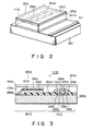
- Fig. 2 is an enlarged view of the main part of the image reader 101 of Fig. 1.
- a first semiconductor chip 111 a and a second semiconductor chip 111 b are linearly formed on an insulating holding substrate 301 in such a manner that their edges are connected to each other.
- a light receiving element section 151a which comprises a plurality of light receiving elements 153a formed on a main surface of a transparent insulating substrate 123a in an array manner and a driving circuit 131 a for driving the light receiving element section 151 a.
- a cover glass 181 a is formed on the light receiving element section 151 a and the driving circuit 131 a to protect these parts such as the light receiving elements and maintain the distance between the document and the light receiving elements at substantially 50 flm.
- a surface light source 121 a for lighting a document which is formed of a thin film electroluminescence element.
- the first semiconductor chip 111 a is structured as mentioned above.
- the second semiconductor chip 111 b (not shown) is structured in the same manner as the first semiconductor chip 111a.
- the semiconductor chips 111 a and 111b will be explained with reference to the schematic cross section of the first semiconductor chip 111 a of Fig.
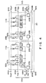
- Fig. 3 is a schematic cross section showing the light receiving element section 151 a provided on the transparent insulating substrate 123a made of glass and a thin film transistor 147a (hereinafter called "TFT") constituting the driving circuit 131 a.
- TFT thin film transistor
- the light receiving element section 151 a comprises a plurality of individual electrodes 154a formed of chromium (Cr), an amorphous silicon layer (a - Si) 155a provided on the individual electrodes 154a, an amorphous silicon carbide layer (a - SiC) 156a provided on the amorphous silicon layer 155a to prevent a leak current, an indium tin oxide (ITO) 157a layered in common on the amorphous silicon layer 155a, and a common electrode 158a connected to ITO 157a.
- Cr chromium
- a - Si amorphous silicon layer
- a - SiC amorphous silicon carbide layer
- ITO indium tin oxide
- the thin film transistor 147a which constitutes the driving circuit 131a, comprises an active layer 133a formed of polycrystalline silicon, an insulating film 135a partially formed on the active layer 133a by thermal oxidation of the polycrystalline silicon, and a gate electrode 137a formed of doped polysilicon.
- a source region 133b of the active layer 133a or a drain region 133c are formed by that an activator is ion-implanted by a self-alignment method and activated.
- An another insulating film 139a is formed on the peripheral portion of the gate electrode 137a.
- a source electrode 141a which is formed of aluminum Al, or a drain electrode 143a is formed on the source region 133b or the drain region 133c.
- the protection glass 181 a via an adhesive layer 171 a.
- a document 401 is made closer to the light receiving element sections 151 a and 151 b and passed thereon by a platen roller (not shown).
- the series arrangement of the first and second semi- conductor chips, which are placed outside of a document passing region 403 allowing a document 401 to be passed, is connected to input/output (10) pads 321 a and 321b. Both ends of the I/O pads 321a a and 321 are formed on a holding substrate 301 by bonding wires.
- input/output pads 321a a and 321 are connected in series by a lead wire 311 formed on the surface of the holding substrate 301.
- the input/output pads 321 a and 321 b may be connected in series by the lead wire 311 in such a manner that the lead wire 311 is formed on the rear surface of the holding substrate 301 or in the holding substrate 301.
- the image reader 101 wherein the first and second semiconductor chips 111 a and 111b comprising the light receiving element section 151 a and the driving circuit 131 a are connected in series, information on the document 401 can be read in a state that the document is sufficiently made closer to each light receiving element 153a even if the document 401 is large-sized.
- the chip widths of the first and second semiconductor chips 111 a and 111 b can be formed to be about 1 mm, the reader can be miniaturized. Also, since a plurality of semi-conductor chips 111 a a and 111 can be surely formed out of one substrate, the manufacturing cost of the reader 1 can be reduced.
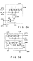
- Fig. 4 shows one example of an equivalent circuit of the above-mentioned reader 101.
- the reader 101 will be explained with reference to the equivalent circuit of Fig. 4.
- Voltage of + 5 V is applied to a VDD terminal 203a of the first semiconductor chip 11a a and an inverting input terminal (not shown) of an inverting amplifier or an operational amplifier (not shown) using an arithmetic amplifier (not shown) is connected to an SOUT terminal 201a.
- the light receiving element 161 a is provided so that a reverse bias is applied to the portion between the VDD terminal 203 and the SOUT terminal 201a.
- TFT 147a is provided between the light receiving element 161a a and the VDD terminal 203a so that the operation of the light receiving element 161a a can be controlled.
- the gate electrode 137a of TFT 147a (Fig. 3) is connected to the output of D-typed flip-flop circuits 211a a corresponding to each TFT 147a.
- the on/off control of TFT 147a is performed in accordance with the signal of the flip-flop circuit 211 a.
- the flip-flop circuits 211a a corresponding to each TFT 147a are respectively connected in series.
- the connection of the flip-flop circuits 211 a is made so that a clock signal is input thereto from a CK terminal 205a.
- the connection of the flip-flop circuits 211 a corresponding to the first light sensitive elements 153b is made so that a shift resister input signal is input thereto from a DIN terminal 207a via shift register input circuit 213a.
- an output which is sent from the flip-flop circuits 211 a to drive n th light receiving element 161a a of the first semiconductor chip 111a, is connected to a gate electrode (not shown) of n th TFT 147a and the first I/O terminal 209a via a shift register output circuit 215a.
- each TFT 147b The gate electrode (not shown) of each TFT 147b is connected to the output sent from D-typed second flip-flop circuits 211 corresponding to the second TFTs 147b.
- Each TFT 147b performs ON/OFF operation in accordance with a signal sent from the second flip-flop circuit 211 b.
- the flip-flop circuits 211b corresponding to each TFT 147b are respectively connected in series.
- the connection of the flip-flop circuits 211 b is made so that a clock signal is input thereto from a second CK terminal 205b similar to the case wherein the clock signal is input to the first semi- conductor chip 111 a.
- connection of the flip-flop circuits 211 b corresponding to the second light receiving elements 153b is made so that a shift resister input signal is input thereto via a first I/O pad 321a of the first semiconductor chip 111 a, a second I/0 pad 321 b connected by a lead wire 311 on the holding substrate 301, and a second shift register input circuit 213b connected to the second I/O pad 321 b.
- an output which is sent from the flip-flop circuits 211 b to drive n th light receiving element 153b of the second semiconductor chip 111 b, is connected to a gate electrode (not shown) of n th TFT 147b and a second DOUT terminal 207b via a second shift register output circuit 215b.
- TFTs 147a and 147b are turned on, the reverse bias voltage is applied to the light receiving elements 153a and 153b, and a parasitic capacity of the light receiving elements 153a and 153b is charged. Then, if TFTs 147a and 147b are turned off with respect to the signal sent from the flip-flop circuits 211 a and 211b, the parasitic capacity stored in the light receiving elements 153a and 153b is discharged. If TFTs 147a and 147b are turned on again after a predetermined cycle of time, the electric charge, which was discharged in accordance with quantity of light, is stored again in the light receiving elements 153a and 153b.
- the TFTs 147a and 147b are sequentially turned on, when one picture element as shown in Fig. 6A is inputted into the shift register at the predetermined cycle.
- the discharging current is read from SOUT terminals 201 a and 201b, thereby information on the document 401 shown in Fig. 1 can be read.
- connection of the first semiconductor chip 111 a to the second semiconductor chip 111 is made in such a manner that the first I/0 pad 321 a is connected to the second I/O pad 321 b by the lead wire 311 formed on the holding substrate 301.
- the Schmit triger circuit and an output driver circuit is provided, thereby influence of noise, which is caused by the elongation of the pattern of the first and second I/O pads 321 a and 321 b, can be overcome.
- the shift register input signal may be distorted by resistance of the lead wire 311 or superimposed.
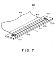
- waveform shaping circuits 221 and 231 may provided as shown in Fig. 5.
- the waveform shaping circuit 221 which is provided in place of the shift register output circuit 215a of the first semiconductor chip 111a, comprises an OR circuit 223 in which the output of n th - second flip-flop circuit and that of n th - third flip-flop circuit are connected, and a buffer circuit 225 which is connected to the OR circuit 223.
- the waveform shaping circuit 231 which is provided in place of the shift input circuit 213b of the second semiconductor chip 111 b, comprises a buffer circuit 233, which is connected to the output sent from the waveform shaping circuit 221 via the second I/O pad 321 b, two flip-flop circuits 235, 237, which are connected to the buffer circuit 233 in series, and an AND circuit to which the outputs of the flip-flop circuits 235 and 237. Then, the clock signal having twice the cycle of the clock signal, which is input from the second CK terminal 205, is input to the third CK terminal 210.
- the clock signal which is input from the second CK terminal 205b, is connected to the second flip-flop circuit 237.
- the shift register input signal which is input from the Din terminal 207a, is synchronized with the clock signal shown in Fig. 61, which is input from the first CK terminal 205a.
- the output signal as shown in Fig. 6A can be obtained from n th - third flip-flop circuit 211 a
- the output signal as shown in Fig. 6B can be obtained from n th - second flip-flop circuit 211 a.
- the OR of these output signals is output from the OR circuit 223 shown in Fig. 6C.
- the output signal will have a long rise and fall time as shown in Fig. 6D after passing through the buffer circuit 225.
- the above signal is input to the flip-flop circuit 235, which is operated by the clock signal shown in Fig. 61 having double cycle sent from the third CK terminal 210, after passing through the buffer circuit 233 of the waveform shaping circuit 231 of the second semiconductor chip 111 b.
- the waveform-shaped signal is input to an AND circuit 239 and the flip-flop circuit 237.
- Fig. 6F is input to AND circuit 239.
- the output sent from AND circuit 239 is synchronized with the clock signal input from the second CK terminal 205b as shown in Fig. 6G. Thereby, the signal, which is sufficiently waveform-shaped, is input to the first flip-flop circuit 211 b.
- the shift register input signal is not distorted by the lead wire 311, which connects the first semiconductor chip 111 a to the second semiconductor chip 111 b, even if the reader 101 is structured by sufficiently large first semiconductor chip 111a or second semiconductor chip 111 b to be able to read sufficiently large document 401.
- Fig. 7 is a perspective view showing schematically a thermal print head 501 according to the second embodiment of the present invention
- Fig. 8 is a perspective view showing an enlarged main part of the thermal print head 501 of Fig. 7.
- a first semiconductor chip 511 a and a second semiconductor chip 511b are linearly formed on an insulating holding substrate 701 in the same manner as of that of the reader 101.
- the first and second semiconductor chips 511 a and 511b are connected in such a manner that an output pad and an input pad are connected to a lead wire 711 formed on a holding substrate 701 by bonding wires.
- the first semiconductor chip 511a comprises a heat resisting section 551a a mainly formed in an array manner and a driving circuit 531 a for driving the heat resisting section 551.
- the second semi- conductor chip 511 b is structured similar to the first semiconductor chip 511 a.
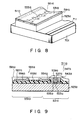
- Fig. 9 is a schematic cross sectional view of the first semiconductor chip 511a a constituting the above-mentioned the thermal printing head.
- the heat resisting section 551 a and the driving circuit 531 a of the respective semiconductor chips 511 a and 511b formed on a glass substrate 523 are structured as follows.
- a resisting member 555a formed of Ta - Si0 2 is formed between a common electrode 557a and an individual electrode 554a extended from the driving circuit 531a.
- the resisting member 555a may be formed of polycrystalline silicon film.
- an SNZY film 556a (non-crystalline member consisting of Si, N, Zr, Yi) is formed between the glass substrate 523a and the resisting member 555a.
- This embodiment shows the example in which SNZY film 556a is used.
- a film of silicon oxide or silicon carbide may be used.
- the driving circuit 531a a comprises a plurality of TFTs 547a.
- An active layer 533a is formed of polycrystalline silicon.
- An insulating film 535a which is partially formed on the active layer 533a, is formed of a thermal oxidation film of the polycrystalline silicon.
- a gate electrode 537a is formed of dope polysilicon.
- a source region 533a of the active layer 533a or a drain region 533c are formed by that an activator is ionimplanted by a self-alignment system and activated.
- a source electrode 554a which is formed of aluminum At to be integral with the individual electrode 554a, or a drain electrode 543a is formed on the source region 533b and the drain region 533c.
- the document 401 can be passed while contacting the heat resisting section 551a a and the shape of the apparatus can be made longer.
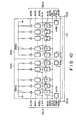
- Fig. 10 is one example of an equivalent circuit of the thermal print head of the second embodiment. The operation of the thermal print head 501 of this embodiment will be explained in detail.
- the driving circuits 531 a and 531 b comprise shift registers 611 and 611b, a latch circuits 615a and 615b, and drivers 613a and 613b.
- An image signal is synchronized with a clock signal, which is input from a CK terminal 605a of the first semiconductor chip 511 a, via a shift register input circuit 617a from an SIN terminal 607a.
- the image signal is sequentially transmitted on the respective flip-flop circuits of the shift register 611a, and reaches to the flip-flop circuit of the final state of the shift register 611 a of the first semiconductor chip 511 a. Then, the image signal reaches to the lead wire 711 via the shift register output circuit 619a, an input/output (I/O) terminal 609a and an I/0 pad 721a. Further, the image signal is input to the shift register input circuit 617b of the second semiconductor chip 511 via an I/O pad 721 b and an I/O terminal 609b from the lead wire 711. Moreover, the image signal is synchronized with the clock signal, which is input from the second CK terminal 605b, and sequentially transmitted on the flip-flop circuit constituting the shift register 611 b of the second semiconductor chip 511b.
- the above-transmitted image signal is held in the latch circuits 615a and 615b of the first and second semiconductor chips 511 a and 511 b. Then, if an ON signal is applied thereto from LA terminals 603a and 603b, a predetermined voltage is applied to the resisting members 555a and 555b via drivers 613a and 613b, thereby information is recorded in the medium.
- information can be clearly recorded by providing an ENABLE terminal in the drivers 613a and 613b (not shown) and controlling the pulse width sent from the output signal.
- a divisional driving can be performed in one line by dividing an ENABLE signal.
- the shift register input signal may be distorted by resistance of the lead wire 711 or superimposed.
- a line driving circuit and a line receiving circuit are used in place of the first shift register output circuit 619a and the second shift register input circuit 617b, thereby the high speed recording can be attained.
- the distortion of the wave-form can be shaped by providing an OR circuit (not shown) in which the signal sent from the first shift register output circuit 619a and the output sent from a reference voltage generating circuit (not shown) are connected.
- the thermal print head 501 information can be clearly recorded in the large-sized document such as A4 or B4-sized document. Also, even if the width of the respective semiconductor chips 511 a and 511 b is made small, the connection between the first and second semi- conductor chips 511 a and 511b can be made. Therefore, a large number of semiconductor chips 511 a and 511 b can be formed out of one substrate, and the manufacturing cost of the apparatus can be reduced. Also, the reduction of the size of the apparatus can be attained.
- the connection between the semi- conductor chips is made in the region outside the medium passing region, the medium can be transferred while being made sufficiently closer to the semiconductor chips. Therefore, information reading or recording can be performed with high accuracy.
- connection between the semi- conductor chips having small chip widths can be made and the size of the apparatus can be reduced. Also, since the semiconductor chips having small chip widths can be used, a large number of semiconductor chips can be obtained from one substrate and the manufacturing cost of the apparatus can be reduced.
Landscapes
- Engineering & Computer Science (AREA)
- Multimedia (AREA)
- Signal Processing (AREA)
- Facsimile Heads (AREA)
- Electronic Switches (AREA)
- Solid State Image Pick-Up Elements (AREA)
Applications Claiming Priority (4)
| Application Number | Priority Date | Filing Date | Title |
|---|---|---|---|
| JP5486790 | 1990-03-08 | ||
| JP54867/90 | 1990-03-08 | ||
| JP2317699A JPH03289759A (ja) | 1990-03-08 | 1990-11-26 | 半導体装置 |
| JP317699/90 | 1990-11-26 |
Publications (3)
| Publication Number | Publication Date |
|---|---|
| EP0445814A2 true EP0445814A2 (fr) | 1991-09-11 |
| EP0445814A3 EP0445814A3 (en) | 1992-08-19 |
| EP0445814B1 EP0445814B1 (fr) | 1997-05-28 |
Family
ID=26395689
Family Applications (1)
| Application Number | Title | Priority Date | Filing Date |
|---|---|---|---|
| EP91103505A Expired - Lifetime EP0445814B1 (fr) | 1990-03-08 | 1991-03-07 | Dispositif avec une suite de plaquettes semi-conductrices qui son interconnectées électriquement les unes aux autres |
Country Status (4)
| Country | Link |
|---|---|
| US (2) | US5260813A (fr) |
| EP (1) | EP0445814B1 (fr) |
| JP (1) | JPH03289759A (fr) |
| DE (1) | DE69126222T2 (fr) |
Families Citing this family (3)
| Publication number | Priority date | Publication date | Assignee | Title |
|---|---|---|---|---|
| US5452001A (en) * | 1993-10-22 | 1995-09-19 | Xerox Corporation | Serial pixel readout scheme for butted sensor chips in multi-chip input scanner |
| US5625498A (en) * | 1995-08-22 | 1997-04-29 | Taiwan Liton Electronic Co Ltd | Lens assembly for optical scanners |
| JPH10285331A (ja) * | 1997-04-10 | 1998-10-23 | Canon Inc | イメージセンサおよびこのイメージセンサを用いた情報処理装置 |
Family Cites Families (12)
| Publication number | Priority date | Publication date | Assignee | Title |
|---|---|---|---|---|
| US4562485A (en) * | 1979-08-10 | 1985-12-31 | Canon Kabushiki Kaisha | Copying apparatus |
| JPS596664A (ja) * | 1982-07-02 | 1984-01-13 | Toshiba Corp | 画像読取り装置 |
| IT1183815B (it) * | 1985-05-03 | 1987-10-22 | Olivetti & Co Spa | Dispositivo di lettura digitale di documenti per apparecchiature di trasmissione e o riproduzione di immagini con compensazione in frequenza dei segnali di lettura |
| JPH0736593B2 (ja) * | 1985-08-01 | 1995-04-19 | セイコーエプソン株式会社 | 密着型イメ−ジセンサ |
| JPH0771171B2 (ja) * | 1985-08-01 | 1995-07-31 | セイコーエプソン株式会社 | 密着型イメ−ジセンサ |
| DE3544182A1 (de) * | 1985-12-13 | 1987-06-19 | Heimann Gmbh | Kontaktbildsensorzeile |
| JPS62213261A (ja) * | 1986-03-14 | 1987-09-19 | Canon Inc | 長尺素子アレイ部材 |
| JPS62229970A (ja) * | 1986-03-31 | 1987-10-08 | Toshiba Corp | イメ−ジセンサ |
| EP0246481B1 (fr) * | 1986-05-13 | 1990-12-27 | Heimann GmbH | Rangée de capteurs d'image à contact |
| US5028935A (en) * | 1986-11-17 | 1991-07-02 | Calcomp Group, Sanders Associates, Inc. | Wide format thermal recording device |
| JPS642376A (en) * | 1987-06-25 | 1989-01-06 | Sony Corp | Photosensor |
| JPH0777261B2 (ja) * | 1989-07-10 | 1995-08-16 | 三菱電機株式会社 | 固体撮像装置及びその組立方法 |
-
1990
- 1990-11-26 JP JP2317699A patent/JPH03289759A/ja active Pending
-
1991
- 1991-03-07 EP EP91103505A patent/EP0445814B1/fr not_active Expired - Lifetime
- 1991-03-07 DE DE69126222T patent/DE69126222T2/de not_active Expired - Fee Related
- 1991-03-07 US US07/666,047 patent/US5260813A/en not_active Expired - Fee Related
-
1992
- 1992-08-25 US US07/934,271 patent/US5280304A/en not_active Expired - Fee Related
Also Published As
| Publication number | Publication date |
|---|---|
| DE69126222T2 (de) | 1998-01-02 |
| US5280304A (en) | 1994-01-18 |
| JPH03289759A (ja) | 1991-12-19 |
| US5260813A (en) | 1993-11-09 |
| EP0445814B1 (fr) | 1997-05-28 |
| DE69126222D1 (de) | 1997-07-03 |
| EP0445814A3 (en) | 1992-08-19 |
Similar Documents
| Publication | Publication Date | Title |
|---|---|---|
| EP0441541B1 (fr) | Dispositif de conversion photoélectrique | |
| EP0600853A2 (fr) | Appareil pour l'enregistrement optique d'information | |
| JP3923728B2 (ja) | 画像読み書き一体ヘッドおよびこれを備えた画像処理装置 | |
| US5040074A (en) | Full-width simultaneous read/write copier | |
| US6952273B1 (en) | Image processing apparatus having an image reading unit and a printing unit on one side of a substrate | |
| EP0445814B1 (fr) | Dispositif avec une suite de plaquettes semi-conductrices qui son interconnectées électriquement les unes aux autres | |
| US4675534A (en) | Optical reader with two substrates | |
| US5196721A (en) | Image reading device | |
| US6222581B1 (en) | Picture reading/writing head and integrated circuit used for the same | |
| US4868669A (en) | Integrated input/output device | |
| JPH0514600A (ja) | 原稿読み取り装置 | |
| JPH1051587A (ja) | 画像読み書きヘッド | |
| US5717502A (en) | Image reading device and information processor having the image reading device | |
| JPS6217877B2 (fr) | ||
| JPH022299B2 (fr) | ||
| JPH04168870A (ja) | 画像読取装置 | |
| JP3074042B2 (ja) | イメージセンサおよび情報処理装置 | |
| JPH04168869A (ja) | 画像読取装置 | |
| JPH04172760A (ja) | 画像読取装置 | |
| JPH02162870A (ja) | 画像入出力デバイス | |
| JPH07107931B2 (ja) | 光電変換装置の製造法 | |
| JPH0537714A (ja) | 光電変換装置 | |
| JPH05244352A (ja) | イメージセンサ | |
| JPH04142860A (ja) | イメージセンサおよびそれを用いた情報処理装置 | |
| JPH03263373A (ja) | 画像入出力デバイス |
Legal Events
| Date | Code | Title | Description |
|---|---|---|---|
| PUAI | Public reference made under article 153(3) epc to a published international application that has entered the european phase |
Free format text: ORIGINAL CODE: 0009012 |
|
| 17P | Request for examination filed |
Effective date: 19910404 |
|
| AK | Designated contracting states |
Kind code of ref document: A2 Designated state(s): DE FR GB |
|
| PUAL | Search report despatched |
Free format text: ORIGINAL CODE: 0009013 |
|
| AK | Designated contracting states |
Kind code of ref document: A3 Designated state(s): DE FR GB |
|
| 17Q | First examination report despatched |
Effective date: 19940511 |
|
| GRAG | Despatch of communication of intention to grant |
Free format text: ORIGINAL CODE: EPIDOS AGRA |
|
| GRAH | Despatch of communication of intention to grant a patent |
Free format text: ORIGINAL CODE: EPIDOS IGRA |
|
| GRAH | Despatch of communication of intention to grant a patent |
Free format text: ORIGINAL CODE: EPIDOS IGRA |
|
| GRAA | (expected) grant |
Free format text: ORIGINAL CODE: 0009210 |
|
| AK | Designated contracting states |
Kind code of ref document: B1 Designated state(s): DE FR GB |
|
| REF | Corresponds to: |
Ref document number: 69126222 Country of ref document: DE Date of ref document: 19970703 |
|
| ET | Fr: translation filed | ||
| PLBE | No opposition filed within time limit |
Free format text: ORIGINAL CODE: 0009261 |
|
| STAA | Information on the status of an ep patent application or granted ep patent |
Free format text: STATUS: NO OPPOSITION FILED WITHIN TIME LIMIT |
|
| 26N | No opposition filed | ||
| REG | Reference to a national code |
Ref country code: GB Ref legal event code: 746 Effective date: 19981008 |
|
| REG | Reference to a national code |
Ref country code: FR Ref legal event code: D6 |
|
| REG | Reference to a national code |
Ref country code: GB Ref legal event code: IF02 |
|
| PGFP | Annual fee paid to national office [announced via postgrant information from national office to epo] |
Ref country code: FR Payment date: 20080311 Year of fee payment: 18 |
|
| PGFP | Annual fee paid to national office [announced via postgrant information from national office to epo] |
Ref country code: GB Payment date: 20090304 Year of fee payment: 19 |
|
| PGFP | Annual fee paid to national office [announced via postgrant information from national office to epo] |
Ref country code: DE Payment date: 20090306 Year of fee payment: 19 |
|
| REG | Reference to a national code |
Ref country code: FR Ref legal event code: ST Effective date: 20091130 |
|
| PG25 | Lapsed in a contracting state [announced via postgrant information from national office to epo] |
Ref country code: FR Free format text: LAPSE BECAUSE OF NON-PAYMENT OF DUE FEES Effective date: 20091123 |
|
| GBPC | Gb: european patent ceased through non-payment of renewal fee |
Effective date: 20100307 |
|
| PG25 | Lapsed in a contracting state [announced via postgrant information from national office to epo] |
Ref country code: DE Free format text: LAPSE BECAUSE OF NON-PAYMENT OF DUE FEES Effective date: 20101001 |
|
| PG25 | Lapsed in a contracting state [announced via postgrant information from national office to epo] |
Ref country code: GB Free format text: LAPSE BECAUSE OF NON-PAYMENT OF DUE FEES Effective date: 20100307 |