EP0445888A2 - Dispositif semi-conducteur du type IGBT ayant une tension de claquage inverse élevée et procédé de fabrication correspondant - Google Patents
Dispositif semi-conducteur du type IGBT ayant une tension de claquage inverse élevée et procédé de fabrication correspondant Download PDFInfo
- Publication number
- EP0445888A2 EP0445888A2 EP91200462A EP91200462A EP0445888A2 EP 0445888 A2 EP0445888 A2 EP 0445888A2 EP 91200462 A EP91200462 A EP 91200462A EP 91200462 A EP91200462 A EP 91200462A EP 0445888 A2 EP0445888 A2 EP 0445888A2
- Authority
- EP
- European Patent Office
- Prior art keywords
- layer
- conductivity
- chip
- semiconductor device
- type
- Prior art date
- Legal status (The legal status is an assumption and is not a legal conclusion. Google has not performed a legal analysis and makes no representation as to the accuracy of the status listed.)
- Withdrawn
Links
- 238000000034 method Methods 0.000 title claims description 14
- 239000004065 semiconductor Substances 0.000 title claims 9
- 230000015556 catabolic process Effects 0.000 title abstract description 9
- VYPSYNLAJGMNEJ-UHFFFAOYSA-N Silicium dioxide Chemical compound O=[Si]=O VYPSYNLAJGMNEJ-UHFFFAOYSA-N 0.000 claims description 17
- 239000000758 substrate Substances 0.000 claims description 15
- 238000002513 implantation Methods 0.000 claims description 13
- ZOXJGFHDIHLPTG-UHFFFAOYSA-N Boron Chemical compound [B] ZOXJGFHDIHLPTG-UHFFFAOYSA-N 0.000 claims description 11
- 229910052796 boron Inorganic materials 0.000 claims description 11
- 238000004519 manufacturing process Methods 0.000 claims description 11
- 238000009792 diffusion process Methods 0.000 claims description 9
- 239000002019 doping agent Substances 0.000 claims description 9
- 238000009413 insulation Methods 0.000 claims description 9
- 238000001259 photo etching Methods 0.000 claims description 8
- 229910052710 silicon Inorganic materials 0.000 claims description 8
- 239000010703 silicon Substances 0.000 claims description 8
- XUIMIQQOPSSXEZ-UHFFFAOYSA-N Silicon Chemical compound [Si] XUIMIQQOPSSXEZ-UHFFFAOYSA-N 0.000 claims description 7
- 229910052681 coesite Inorganic materials 0.000 claims description 7
- 229910052906 cristobalite Inorganic materials 0.000 claims description 7
- 239000000377 silicon dioxide Substances 0.000 claims description 7
- 235000012239 silicon dioxide Nutrition 0.000 claims description 7
- 229910052682 stishovite Inorganic materials 0.000 claims description 7
- 229910052905 tridymite Inorganic materials 0.000 claims description 7
- 230000001590 oxidative effect Effects 0.000 claims description 6
- 230000015572 biosynthetic process Effects 0.000 claims description 4
- 230000012010 growth Effects 0.000 claims description 4
- BHEPBYXIRTUNPN-UHFFFAOYSA-N hydridophosphorus(.) (triplet) Chemical compound [PH] BHEPBYXIRTUNPN-UHFFFAOYSA-N 0.000 claims description 2
- 229910021421 monocrystalline silicon Inorganic materials 0.000 claims description 2
- 229910052751 metal Inorganic materials 0.000 description 5
- 239000002184 metal Substances 0.000 description 5
- 238000002161 passivation Methods 0.000 description 5
- 230000003647 oxidation Effects 0.000 description 4
- 238000007254 oxidation reaction Methods 0.000 description 4
- 230000005684 electric field Effects 0.000 description 3
- 239000004411 aluminium Substances 0.000 description 2
- 229910052782 aluminium Inorganic materials 0.000 description 2
- 239000011521 glass Substances 0.000 description 2
- 229910052814 silicon oxide Inorganic materials 0.000 description 2
- 150000001398 aluminium Chemical class 0.000 description 1
- XAGFODPZIPBFFR-UHFFFAOYSA-N aluminium Chemical compound [Al] XAGFODPZIPBFFR-UHFFFAOYSA-N 0.000 description 1
- 230000003698 anagen phase Effects 0.000 description 1
- 229910052787 antimony Inorganic materials 0.000 description 1
- WATWJIUSRGPENY-UHFFFAOYSA-N antimony atom Chemical compound [Sb] WATWJIUSRGPENY-UHFFFAOYSA-N 0.000 description 1
- 229910052785 arsenic Inorganic materials 0.000 description 1
- RQNWIZPPADIBDY-UHFFFAOYSA-N arsenic atom Chemical compound [As] RQNWIZPPADIBDY-UHFFFAOYSA-N 0.000 description 1
- 239000000356 contaminant Substances 0.000 description 1
- 239000003989 dielectric material Substances 0.000 description 1
- 150000002500 ions Chemical class 0.000 description 1
- 239000000463 material Substances 0.000 description 1
- 230000002093 peripheral effect Effects 0.000 description 1
Images


Classifications
-
- H—ELECTRICITY
- H10—SEMICONDUCTOR DEVICES; ELECTRIC SOLID-STATE DEVICES NOT OTHERWISE PROVIDED FOR
- H10D—INORGANIC ELECTRIC SEMICONDUCTOR DEVICES
- H10D64/00—Electrodes of devices having potential barriers
- H10D64/111—Field plates
-
- H—ELECTRICITY
- H10—SEMICONDUCTOR DEVICES; ELECTRIC SOLID-STATE DEVICES NOT OTHERWISE PROVIDED FOR
- H10D—INORGANIC ELECTRIC SEMICONDUCTOR DEVICES
- H10D12/00—Bipolar devices controlled by the field effect, e.g. insulated-gate bipolar transistors [IGBT]
- H10D12/01—Manufacture or treatment
- H10D12/031—Manufacture or treatment of IGBTs
- H10D12/032—Manufacture or treatment of IGBTs of vertical IGBTs
-
- H—ELECTRICITY
- H10—SEMICONDUCTOR DEVICES; ELECTRIC SOLID-STATE DEVICES NOT OTHERWISE PROVIDED FOR
- H10D—INORGANIC ELECTRIC SEMICONDUCTOR DEVICES
- H10D12/00—Bipolar devices controlled by the field effect, e.g. insulated-gate bipolar transistors [IGBT]
- H10D12/411—Insulated-gate bipolar transistors [IGBT]
- H10D12/441—Vertical IGBTs
-
- H—ELECTRICITY
- H10—SEMICONDUCTOR DEVICES; ELECTRIC SOLID-STATE DEVICES NOT OTHERWISE PROVIDED FOR
- H10D—INORGANIC ELECTRIC SEMICONDUCTOR DEVICES
- H10D62/00—Semiconductor bodies, or regions thereof, of devices having potential barriers
- H10D62/10—Shapes, relative sizes or dispositions of the regions of the semiconductor bodies; Shapes of the semiconductor bodies
- H10D62/13—Semiconductor regions connected to electrodes carrying current to be rectified, amplified or switched, e.g. source or drain regions
- H10D62/141—Anode or cathode regions of thyristors; Collector or emitter regions of gated bipolar-mode devices, e.g. of IGBTs
- H10D62/142—Anode regions of thyristors or collector regions of gated bipolar-mode devices
Definitions
- the present invention relates to an MOS power device with conductivity modulation, otherwise known as Insulated Gate Bipolar Transistor (IGBT), having a high reverse breakdown voltage of the anode junction.
- IGBT Insulated Gate Bipolar Transistor
- the reverse breakdown voltage of the anode junction is quite limited and in particular is lower than about 5V.
- the edge of the anode junction (junction between the substrate and the overlying epitaxial layer) is allocated on the side edge of the chip, after cutting of the latter. Consequently, since the edge of the junction is not in any way passivated and there is no structure (of the field plate, bevel etc. type) permitting lowering of the electric field value, breakdown voltage of this junction is extremely low.
- a solution for raising said voltage could be adoption of a passivation method similar to the one described in Italian patent No. 1,202,311 and in corresponding U.S. patent No. 4,805,004 with reference to the collector-base junction of a bipolar power transistor (see FIG. 4 of said patents, reproduced herein in FIG. 2).
- Said method employs a structure similar to the Mesa structure but, in place of the peripheral channel trenched chemically, calls for a deep diffusion (51) of the same type of conductivity as the substrate.
- This type of structure cannot be used for high voltage IGBT devices with high thickness of the epitaxial layer, because realizing very deep diffused regions such as to reach the substrate would require extremely long diffusion time, even several days, so involving high costs.
- Another solution could be to obtain the device by Mesa technology so as to excavate a trench all around the chip sufficiently deep to uncover the anode junction and then passivate the junction surface with a layer of dielectric material, for example glass.
- the object of the present invention is an IGBT device free from the above mentioned drawbacks, with high reverse breakdown voltage of the anode junction comparable to the BVdss (Breakdown Voltage drain-source shorted gate) of the device.
- the device in accordance with the invention is realized in a chip comprising a substrate of a first type of conductivity and an overlying epitaxial layer having conductivity of the opposite type, whose junction constitutes the anode junction of the device, and is characterized by the presence along the periphery of the chip of a side insulation region of the top-bottom type formed in such a manner as to cause the anode junction to return upward laterally until it terminates in a surface zone of the chip covered in succession by a layer of SiO2 and a metallic layer constituting the field-plate of the device.
- FIG.1 shows, as already mentioned, an example of a known structure of an IGBT device.
- Said figure 1 shows how the edge of the anode junction "r" is on the side edge of the chip after cutting the same.
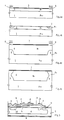
- FIGS. 4a-4d An embodiment process for an N channel MOS device in accordance with the invention is described in FIGS. 4a-4d. It calls for the following phases in sequence.
- the process described above permits obtaining devices with reverse breakdown voltage of approximately 600 V. If it is desired to obtain devices with higher reverse voltage (up to 1200 V), the operational sequence described above should be modified by introducing between phases 8 and 9 the following processes: starting from FIG. 4d there is performed a new photoetching the same as that of FIG. 4c, then follows boron implantation at the frame 12 (FIG. 4e), a nonoxidizing diffusion, removal of the oxide layer and a new epitaxial growth 13 followed by an oxidation (FIG. 4f).
- the present invention permits obtaining devices with much lower reverse voltages (on the order of 50 V) since the anode junction shown in FIG. 5 would be made up of two highly doped regions: the P++ type substrate 21 and the N+ type buffer layer 22 (see FIG. 6d of the following description).
- the critical electrical field and hence the breakdown voltage, which is a function of the dopant concentration, would fall considerably.
- the manufacturing process is modified by inserting after phase 2 (thermal oxidation 3 of the silicon of FIG. 4a) a photoetching and subsequently an implantation and oxidizing diffusion of antimony or arsenic (FIG. 6a o ) and then the sequence of FIGS. 4a, 4b, 4c and 4d, reproduced in FIGS. 6a, 6b, 6c and 6d.
- anode junction at the edges of the chip turns upward, appears at the surface and the device is completed up to obtaining substantially the structure of FIG. 5.
- a layer of silicon oxide 15 is thermally deposited on the edge of the junction and subsequently there is deposited thereon a film 16 of aluminium which, on the outside, contacts the silicon in the region of the P+ ring 9 or in the P+ top-bottom pocket 5, while it lies over the oxide 15 on the inside.
- This aluminium film acts as a field plate, i.e. it widens the electrical field lines inside the N- epitaxial layer.
- FIG. 5 also shows how the finished device allows embodiment of a field plate which inserts perfectly in the edge structure of the IGBT device.
Landscapes
- Insulated Gate Type Field-Effect Transistor (AREA)
- Die Bonding (AREA)
- Electronic Switches (AREA)
- Bipolar Transistors (AREA)
Applications Claiming Priority (2)
| Application Number | Priority Date | Filing Date | Title |
|---|---|---|---|
| IT660690 | 1990-03-08 | ||
| IT6606A IT1241049B (it) | 1990-03-08 | 1990-03-08 | Dispositivo a semiconduttore igbt ad elevata tensione di rottura inversa e relativo processo di fabbricazione |
Publications (2)
| Publication Number | Publication Date |
|---|---|
| EP0445888A2 true EP0445888A2 (fr) | 1991-09-11 |
| EP0445888A3 EP0445888A3 (en) | 1991-11-13 |
Family
ID=11121311
Family Applications (1)
| Application Number | Title | Priority Date | Filing Date |
|---|---|---|---|
| EP19910200462 Withdrawn EP0445888A3 (en) | 1990-03-08 | 1991-03-05 | Igbt semiconductor device with high reverse breakdown voltage and related manufaturing process |
Country Status (3)
| Country | Link |
|---|---|
| EP (1) | EP0445888A3 (fr) |
| JP (1) | JPH065866A (fr) |
| IT (1) | IT1241049B (fr) |
Families Citing this family (4)
| Publication number | Priority date | Publication date | Assignee | Title |
|---|---|---|---|---|
| JP3352840B2 (ja) * | 1994-03-14 | 2002-12-03 | 株式会社東芝 | 逆並列接続型双方向性半導体スイッチ |
| JPH10209447A (ja) * | 1997-01-22 | 1998-08-07 | Toshiba Corp | 半導体スイッチ |
| JP4967200B2 (ja) * | 2000-08-09 | 2012-07-04 | 富士電機株式会社 | 逆阻止型igbtを逆並列に接続した双方向igbt |
| JP2014049694A (ja) * | 2012-09-03 | 2014-03-17 | Renesas Electronics Corp | Igbt |
Family Cites Families (1)
| Publication number | Priority date | Publication date | Assignee | Title |
|---|---|---|---|---|
| IT1218200B (it) * | 1988-03-29 | 1990-04-12 | Sgs Thomson Microelectronics | Procedimento di fabbricazione di un dispositivo semiconduttore mos di poterza a modulazione di conducibilita' (himos) e dispositivi con esso ottenuti |
-
1990
- 1990-03-08 IT IT6606A patent/IT1241049B/it active IP Right Grant
-
1991
- 1991-03-05 EP EP19910200462 patent/EP0445888A3/en not_active Withdrawn
- 1991-03-08 JP JP3067634A patent/JPH065866A/ja active Pending
Also Published As
| Publication number | Publication date |
|---|---|
| EP0445888A3 (en) | 1991-11-13 |
| JPH065866A (ja) | 1994-01-14 |
| IT1241049B (it) | 1993-12-29 |
| IT9006606A0 (it) | 1990-03-08 |
| IT9006606A1 (it) | 1991-09-08 |
Similar Documents
| Publication | Publication Date | Title |
|---|---|---|
| US6825105B2 (en) | Manufacture of semiconductor devices with Schottky barriers | |
| US5429964A (en) | Low on-resistance power MOS technology | |
| US6251730B1 (en) | Semiconductor power device manufacture | |
| KR100468342B1 (ko) | 자기-정렬resurf영역을가진ldmos장치및그제조방법 | |
| US6432775B2 (en) | Trench DMOS transistor structure having a low resistance path to a drain contact located on an upper surface | |
| US5895249A (en) | Integrated edge structure for high voltage semiconductor devices and related manufacturing process | |
| US4038107A (en) | Method for making transistor structures | |
| US8487368B2 (en) | Low voltage power MOSFET device and process for its manufacture | |
| JPS62272570A (ja) | 垂直ゲート半導体装置及びその製造方法 | |
| JPH08264787A (ja) | パワーmosfetのエッジターミネーション方法および構造 | |
| WO2001075960A2 (fr) | Procede pour fabriquer un dispositif dmos a tranchee a tension de seuil reduite | |
| US5960275A (en) | Power MOSFET fabrication process to achieve enhanced ruggedness, cost savings, and product reliability | |
| EP0751573A1 (fr) | Circuit intégré de puissance et procédé de fabrication associé | |
| JP2807114B2 (ja) | シリコン集積回路の製造に於ける欠陥形成の制御方法、酸化膜の品質及び欠陥形成の制御方法、二重拡散集積回路デバイスセルと、集積回路mosfetセルの形成方法 | |
| KR0134887B1 (ko) | 쌍극성 트랜지스터 및 그 제조방법 | |
| US5923065A (en) | Power MOSFET device manufactured with simplified fabrication processes to achieve improved ruggedness and product cost savings | |
| US5729037A (en) | MOSFET structure and fabrication process for decreasing threshold voltage | |
| EP0453026B1 (fr) | Procédé pour la formation d'une région de drain et de collecteur enterrée pour dispositifs semi-conducteurs monolithiques | |
| US7482205B2 (en) | Process for resurf diffusion for high voltage MOSFET | |
| EP0445888A2 (fr) | Dispositif semi-conducteur du type IGBT ayant une tension de claquage inverse élevée et procédé de fabrication correspondant | |
| US7391079B2 (en) | Metal oxide semiconductor device | |
| US4216038A (en) | Semiconductor device and manufacturing process thereof | |
| US5434095A (en) | Method for controlling electrical breakdown in semiconductor power devices | |
| KR100563162B1 (ko) | 반도체장치및그제조방법 | |
| EP0766318A1 (fr) | Semiconducteur dote de dispositifs verticaux de type plan a tension de tenue elevee et procede de production dudit semiconducteur |
Legal Events
| Date | Code | Title | Description |
|---|---|---|---|
| PUAI | Public reference made under article 153(3) epc to a published international application that has entered the european phase |
Free format text: ORIGINAL CODE: 0009012 |
|
| AK | Designated contracting states |
Kind code of ref document: A2 Designated state(s): DE FR GB |
|
| PUAL | Search report despatched |
Free format text: ORIGINAL CODE: 0009013 |
|
| AK | Designated contracting states |
Kind code of ref document: A3 Designated state(s): DE FR GB |
|
| 17P | Request for examination filed |
Effective date: 19920317 |
|
| D17Q | First examination report despatched (deleted) | ||
| STAA | Information on the status of an ep patent application or granted ep patent |
Free format text: STATUS: THE APPLICATION IS DEEMED TO BE WITHDRAWN |
|
| 18D | Application deemed to be withdrawn |
Effective date: 19950124 |