EP0446666A2 - Lötverbindungsstruktur auf organischen Substraten und Herstellungsverfahren - Google Patents
Lötverbindungsstruktur auf organischen Substraten und Herstellungsverfahren Download PDFInfo
- Publication number
- EP0446666A2 EP0446666A2 EP91102393A EP91102393A EP0446666A2 EP 0446666 A2 EP0446666 A2 EP 0446666A2 EP 91102393 A EP91102393 A EP 91102393A EP 91102393 A EP91102393 A EP 91102393A EP 0446666 A2 EP0446666 A2 EP 0446666A2
- Authority
- EP
- European Patent Office
- Prior art keywords
- solder
- solder interconnection
- substrate
- filler
- semiconductor device
- Prior art date
- Legal status (The legal status is an assumption and is not a legal conclusion. Google has not performed a legal analysis and makes no representation as to the accuracy of the status listed.)
- Withdrawn
Links
Images
Classifications
-
- H—ELECTRICITY
- H10—SEMICONDUCTOR DEVICES; ELECTRIC SOLID-STATE DEVICES NOT OTHERWISE PROVIDED FOR
- H10W—GENERIC PACKAGES, INTERCONNECTIONS, CONNECTORS OR OTHER CONSTRUCTIONAL DETAILS OF DEVICES COVERED BY CLASS H10
- H10W70/00—Package substrates; Interposers; Redistribution layers [RDL]
- H10W70/60—Insulating or insulated package substrates; Interposers; Redistribution layers
- H10W70/67—Insulating or insulated package substrates; Interposers; Redistribution layers characterised by their insulating layers or insulating parts
- H10W70/69—Insulating materials thereof
- H10W70/695—Organic materials
-
- H—ELECTRICITY
- H10—SEMICONDUCTOR DEVICES; ELECTRIC SOLID-STATE DEVICES NOT OTHERWISE PROVIDED FOR
- H10W—GENERIC PACKAGES, INTERCONNECTIONS, CONNECTORS OR OTHER CONSTRUCTIONAL DETAILS OF DEVICES COVERED BY CLASS H10
- H10W74/00—Encapsulations, e.g. protective coatings
- H10W74/01—Manufacture or treatment
- H10W74/012—Manufacture or treatment of encapsulations on active surfaces of flip-chip devices, e.g. forming underfills
-
- H—ELECTRICITY
- H10—SEMICONDUCTOR DEVICES; ELECTRIC SOLID-STATE DEVICES NOT OTHERWISE PROVIDED FOR
- H10W—GENERIC PACKAGES, INTERCONNECTIONS, CONNECTORS OR OTHER CONSTRUCTIONAL DETAILS OF DEVICES COVERED BY CLASS H10
- H10W74/00—Encapsulations, e.g. protective coatings
- H10W74/10—Encapsulations, e.g. protective coatings characterised by their shape or disposition
- H10W74/15—Encapsulations, e.g. protective coatings characterised by their shape or disposition on active surfaces of flip-chip devices, e.g. underfills
-
- H—ELECTRICITY
- H10—SEMICONDUCTOR DEVICES; ELECTRIC SOLID-STATE DEVICES NOT OTHERWISE PROVIDED FOR
- H10W—GENERIC PACKAGES, INTERCONNECTIONS, CONNECTORS OR OTHER CONSTRUCTIONAL DETAILS OF DEVICES COVERED BY CLASS H10
- H10W74/00—Encapsulations, e.g. protective coatings
- H10W74/40—Encapsulations, e.g. protective coatings characterised by their materials
- H10W74/47—Encapsulations, e.g. protective coatings characterised by their materials comprising organic materials, e.g. plastics or resins
- H10W74/473—Encapsulations, e.g. protective coatings characterised by their materials comprising organic materials, e.g. plastics or resins containing a filler
-
- H—ELECTRICITY
- H10—SEMICONDUCTOR DEVICES; ELECTRIC SOLID-STATE DEVICES NOT OTHERWISE PROVIDED FOR
- H10W—GENERIC PACKAGES, INTERCONNECTIONS, CONNECTORS OR OTHER CONSTRUCTIONAL DETAILS OF DEVICES COVERED BY CLASS H10
- H10W72/00—Interconnections or connectors in packages
- H10W72/071—Connecting or disconnecting
- H10W72/072—Connecting or disconnecting of bump connectors
- H10W72/07231—Techniques
- H10W72/07236—Soldering or alloying
-
- H—ELECTRICITY
- H10—SEMICONDUCTOR DEVICES; ELECTRIC SOLID-STATE DEVICES NOT OTHERWISE PROVIDED FOR
- H10W—GENERIC PACKAGES, INTERCONNECTIONS, CONNECTORS OR OTHER CONSTRUCTIONAL DETAILS OF DEVICES COVERED BY CLASS H10
- H10W72/00—Interconnections or connectors in packages
- H10W72/071—Connecting or disconnecting
- H10W72/072—Connecting or disconnecting of bump connectors
- H10W72/07251—Connecting or disconnecting of bump connectors characterised by changes in properties of the bump connectors during connecting
-
- H—ELECTRICITY
- H10—SEMICONDUCTOR DEVICES; ELECTRIC SOLID-STATE DEVICES NOT OTHERWISE PROVIDED FOR
- H10W—GENERIC PACKAGES, INTERCONNECTIONS, CONNECTORS OR OTHER CONSTRUCTIONAL DETAILS OF DEVICES COVERED BY CLASS H10
- H10W72/00—Interconnections or connectors in packages
- H10W72/20—Bump connectors, e.g. solder bumps or copper pillars; Dummy bumps; Thermal bumps
-
- H—ELECTRICITY
- H10—SEMICONDUCTOR DEVICES; ELECTRIC SOLID-STATE DEVICES NOT OTHERWISE PROVIDED FOR
- H10W—GENERIC PACKAGES, INTERCONNECTIONS, CONNECTORS OR OTHER CONSTRUCTIONAL DETAILS OF DEVICES COVERED BY CLASS H10
- H10W72/00—Interconnections or connectors in packages
- H10W72/20—Bump connectors, e.g. solder bumps or copper pillars; Dummy bumps; Thermal bumps
- H10W72/251—Materials
- H10W72/252—Materials comprising solid metals or solid metalloids, e.g. PbSn, Ag or Cu
-
- H—ELECTRICITY
- H10—SEMICONDUCTOR DEVICES; ELECTRIC SOLID-STATE DEVICES NOT OTHERWISE PROVIDED FOR
- H10W—GENERIC PACKAGES, INTERCONNECTIONS, CONNECTORS OR OTHER CONSTRUCTIONAL DETAILS OF DEVICES COVERED BY CLASS H10
- H10W72/00—Interconnections or connectors in packages
- H10W72/851—Dispositions of multiple connectors or interconnections
- H10W72/853—On the same surface
- H10W72/856—Bump connectors and die-attach connectors
-
- H—ELECTRICITY
- H10—SEMICONDUCTOR DEVICES; ELECTRIC SOLID-STATE DEVICES NOT OTHERWISE PROVIDED FOR
- H10W—GENERIC PACKAGES, INTERCONNECTIONS, CONNECTORS OR OTHER CONSTRUCTIONAL DETAILS OF DEVICES COVERED BY CLASS H10
- H10W90/00—Package configurations
- H10W90/701—Package configurations characterised by the relative positions of pads or connectors relative to package parts
- H10W90/721—Package configurations characterised by the relative positions of pads or connectors relative to package parts of bump connectors
- H10W90/724—Package configurations characterised by the relative positions of pads or connectors relative to package parts of bump connectors between a chip and a stacked insulating package substrate, interposer or RDL
-
- H—ELECTRICITY
- H10—SEMICONDUCTOR DEVICES; ELECTRIC SOLID-STATE DEVICES NOT OTHERWISE PROVIDED FOR
- H10W—GENERIC PACKAGES, INTERCONNECTIONS, CONNECTORS OR OTHER CONSTRUCTIONAL DETAILS OF DEVICES COVERED BY CLASS H10
- H10W90/00—Package configurations
- H10W90/701—Package configurations characterised by the relative positions of pads or connectors relative to package parts
- H10W90/731—Package configurations characterised by the relative positions of pads or connectors relative to package parts of die-attach connectors
- H10W90/734—Package configurations characterised by the relative positions of pads or connectors relative to package parts of die-attach connectors between a chip and a stacked insulating package substrate, interposer or RDL
-
- Y—GENERAL TAGGING OF NEW TECHNOLOGICAL DEVELOPMENTS; GENERAL TAGGING OF CROSS-SECTIONAL TECHNOLOGIES SPANNING OVER SEVERAL SECTIONS OF THE IPC; TECHNICAL SUBJECTS COVERED BY FORMER USPC CROSS-REFERENCE ART COLLECTIONS [XRACs] AND DIGESTS
- Y10—TECHNICAL SUBJECTS COVERED BY FORMER USPC
- Y10T—TECHNICAL SUBJECTS COVERED BY FORMER US CLASSIFICATION
- Y10T29/00—Metal working
- Y10T29/49—Method of mechanical manufacture
- Y10T29/49002—Electrical device making
- Y10T29/49117—Conductor or circuit manufacturing
- Y10T29/49124—On flat or curved insulated base, e.g., printed circuit, etc.
- Y10T29/4913—Assembling to base an electrical component, e.g., capacitor, etc.
- Y10T29/49144—Assembling to base an electrical component, e.g., capacitor, etc. by metal fusion
-
- Y—GENERAL TAGGING OF NEW TECHNOLOGICAL DEVELOPMENTS; GENERAL TAGGING OF CROSS-SECTIONAL TECHNOLOGIES SPANNING OVER SEVERAL SECTIONS OF THE IPC; TECHNICAL SUBJECTS COVERED BY FORMER USPC CROSS-REFERENCE ART COLLECTIONS [XRACs] AND DIGESTS
- Y10—TECHNICAL SUBJECTS COVERED BY FORMER USPC
- Y10T—TECHNICAL SUBJECTS COVERED BY FORMER US CLASSIFICATION
- Y10T29/00—Metal working
- Y10T29/49—Method of mechanical manufacture
- Y10T29/49002—Electrical device making
- Y10T29/49117—Conductor or circuit manufacturing
- Y10T29/49124—On flat or curved insulated base, e.g., printed circuit, etc.
- Y10T29/4913—Assembling to base an electrical component, e.g., capacitor, etc.
- Y10T29/49146—Assembling to base an electrical component, e.g., capacitor, etc. with encapsulating, e.g., potting, etc.
Definitions
- the present invention is concerned with interconnection structures for joining an integrated semiconductor device to an organic substrate and particularly to a structure for forming solder interconnection joints that exhibit improved fatigue life and stability.
- the present invention is especially concerned with so-called "controlled collapse chip connection” or "C4" that employs solder-bump interconnections. Such is also referred to as the face down or flip-chip bonding.
- C4 controlled collapse chip connection
- the present invention is also concerned with a method of making the interconnection structure.
- Controlled collapse chip connection (C4) or flip-chip technology has been successfully used for over twenty years for interconnecting high I/O (input/output) count and area array solder bumps on the silicon chips to the base rigid ceramic chip carriers, for example alumina carriers.
- the solder bump typically a 95 Pb/5 Sn alloy, provides the means of chip attachment to the rigid ceramic chip carrier for subsequent usage and testing.
- C4 controlled collapse chip connection
- a malleable pad of metallic solder is formed on the semiconductor device contact site and solder joinable sites are formed on the conductors on the rigid chip carrier.
- the device carrier solder joinable sites are surrounded by non-solderable barriers so that when the solder on the semiconductor device contact sites melts, surface tension of the molten solder prevents collapse of the joints and thus holds the semiconductor device suspended above the rigid carrier.
- the integrated circuit semiconductor devices are mounted on rigid supporting substrates made of materials with coefficients of expansion that differ from the coefficient of expansion of the material of the semiconductor device, i.e. silicon.
- the device is formed of monocrystalline silicon with a coefficient of expansion of 2.5 X 10⁻⁶ per °C.
- the substrate is formed of a ceramic material, typically alumina with a coefficient of expansion of 5.8 X 10⁻⁶ per °C.
- the active and passive elements of the integrated semiconductor device inevitably generate heat resulting in temperature fluctuations in both the devices and the supporting substrate since the heat is conducted through the solder bonds.
- the devices and the substrate thus expand and contract in different amounts with temperature fluctuations, due to the different coefficients of expansion. This imposes stresses on the relatively rigid solder terminals.
- the stress on the solder bonds during operation is directly proportional to (1) the magnitude of the temperature fluctuations, (2) the distance of an individual bond from the neutral or central point (DNP), and (3) the difference in the coefficients of expansion of the material of the semiconductor device and the substrate, and inversely proportional to the height of the solder bond, that is the spacing between the device and the support substrate.
- the seriousness of the situation is further compounded by the fact that as the solder terminals become smaller in diameter in order to accommodate the need for greater density, the overall height decreases.
- Patent 4,604,644 discloses a structure for electrically joining a semiconductor device to a support substrate that has a plurality of solder connections where each solder connection is joined to a solder wettable pad on the device and a corresponding solder wettable pad on the rigid support substrate, dielectric organic material disposed between the peripheral area of the device and the facing area of the substrate, which material surrounds at least one outer row and column of solder connections but leaves the solder connections in the central area of the device free of dielectric organic material.
- AI-10 is formed by reacting a diamine such as p,p'diaminodiphenylmethane with trimellitic anhydride or acylchloride of trimellitic anhydride.
- the polymer is further reacted with gamma-amino propyl triethoxy silane (A1100) or ⁇ -(3,4-epoxy cyclohexyl) ethyltrimethoxy silane (A-186).
- the coating material is described in IBM TDB Sept. 1970 P. 825.
- the dielectric material is typically applied by first mixing it with a suitable solvent and then dispensing it along the periphery of the device where it can be drawn in between the device and substrate by capillary action.
- organic substrates generally cannot tolerate processing temperatures of the magnitude that can be tolerated by ceramics.
- the present invention as claimed is concerned with providing C4 solder connections of an integrated semiconductor device on an organic substrate.
- the problem of the tendency of organic substrates to bow and twist with virtually precluded the ability to directly attach such to an integrated semiconductor device by C4 solder connections is compensated for by the present invention.
- the present invention prevents the C4 bonds from breaking and at least significantly minimize the bowing in the localized chip encapsulant area.
- the present invention also compensates for the excessive thermal mismatch between the organic substrates and the semiconductor devices.
- the present invention makes it possible to achieve the desired bonding without including metal in the interior of the substrate such as the copper/Invar/copper. Accordingly, the present invention is suitable for substrates that do not include metal in the interior as well as those containing metals including the conventional copper foil as the metal therein. Of course, if desired, the more elaborate copper/Invar/copper can be used.
- the present invention is concerned with solder interconnection for forming connections between an integrated semiconductor device and an organic substrate.
- the solder interconnection includes a plurality of solder connections that extend from the organic substrate to electrodes on the semiconductor device to form a gap between the carrier substrate and the semiconductor device.
- the gap is filled with a composition obtained from curing a curable composition containing a thermosetting binder and a filler.
- the binder employed has viscosity at normal room temperatures (25°C) of no greater than about 1,000 centipoise.
- the filler has a maximum particle size of 50 microns.
- the binder is resistant to temperatures of at least about 280°C.
- the amount of binder is about 60 to about 25 percent by weight of the total of the binder and filler and, correspondingly, the filler is about 40 to about 75 percent by weight of the total of the binder and filler.
- the present invention is concerned with a method of achieving solder interconnections between a semiconductor device and an organic substrate.
- the method includes attaching the device to the organic substrate by a plurality of solder connections that extend from the organic substrate to electrodes on the semiconductor device to form a gap between the supporting substrate and the semiconductor device.
- the gap is filled with the above disclosed binder-filler composition and the composition is cured.
- the present invention results in C4 interconnections of semiconductor device, onto organic substrates that are at least as resistant to fatigue and in certain cases significantly improved as compared to encapsulated C4 interconnections on ceramic rigid substrates. This is surprising since without the encapsulant as employed in the present invention, the solder bonds on organic substrates are completely unacceptable for thermal cycling to simulate system behavior.
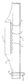
- the figure is a schematic diagram of a solder interconnection pursuant to the present invention.
- numeral 1 represents a semiconductor chip joined to the organic 2 by solder bumps 3 mated to pads 4.
- the encapsulant 7 pursuant to the present invention provides for essentially void free polymer encapsulation of the solder connections thereby assuring highly reliable devices and fills the gap.
- the encapsulant composition required by the present invention contain a binder and a filler.
- Suitable binders include polyepoxides, cyanate esters and prepolymers thereof.
- the thermosetting binders employed in the present invention have viscosities at 25°C of no greater than about 1,000 centipoise and most preferably about 300 to about 450 centipoise.
- compositions employed pursuant to the present invention also include a filler and especially an inorganic filler.
- the particle size of the filler must not be greater than 50 microns or less, preferably about not to be greater than 35 microns and most preferably not to be greater than 25 microns. Most preferably at least about 90 weight % of the particles are no smaller than 0.7 microns. Smaller particle sizes are necessary so that the composite polymer material will readily flow in the gap between the chip and substrate carrier.
- the gap is normally about 25 to about 50 microns but in some cases is somewhat larger such as about 75 to about 125 microns.
- the preferred fillers have average particle size of about 3 to about 5 microns, even though there may be a distribution of a minor amount of some larger particles.
- the filler is at least substantially free of alpha particle emissions such as from the trace amounts of radioactive impurities such as uranium and thorium normally present in conventional silica or quartz fillers.
- the preferred fillers employed have emission rates of less than 0.01 alpha particles/cm2-hr and most preferably less 0.005 alpha particles/cm2-hr.
- the presence of ⁇ -particle emissions primarily caused by the presence of uranium and thorium isotopes in the fillers can generate electron/hole pairs which in turn would be detrimental to the device.
- the preferred filler is high purity fused or amorphous silica or synthetic glass commercial fillers which typically are rounded filler particles.
- a commercially available filler that can be employed is DP4910 from PQ Corporation.
- the preferred filler can be optionally treated with a coupling agent.
- compositions of the present invention contain about 25 to about 60% by weight and preferably about 50 to about 60% by weight of the binder and correspondingly about 40 to about 75% by weight and preferably about 50 to about 60% by weight of the filler. These amounts are based upon the total amounts of binder and filler in the composition.
- the binder includes the polyepoxide
- the compositions employed in the present invention also include a hardening or curing agent.
- the preferred hardeners for the polyepoxides are the anhydrides or organic carboxylic acids.
- the hardening agent is preferably in liquid form. If a solid hardening agent is employed, such should be melted when added to the composition.
- anhydrides are methyltetrahydrophthalic anhydride; hexahydrophthalic anhydride; maleic anhydride, trimellitic anhydride; pyromellitic dianhydride, tetrahydrophthalic anhydride; phthalic anhydride; norbornenedicarboxylic anhydride; nadic methyl anhydride; and methylcyclohexane-1,2-dicarboxylic anhydride.
- the anhydride curing agent is generally employed in amounts constituting on an equivalent basis, about 20% to about 120% of the cycloaliphatic epoxide employed and more usually about 75% to about 100% of the epoxide equivalents.
- the curing agent is employed in amounts of about 89 to about 110 parts by weight per hundred parts of polyepoxy (phr).
- compositions can also include a catalyst to promote the polymerization of the epoxy and/or cyanate ester.
- Suitable catalysts for the epoxy include amines such as the tertiary amine benzyldimethylamine, 1,3-tetramethyl butane diamine, tris (dimethylaminomethyl) phenol, pyridine, and triethylenediamine and acidic catalysts such as stannous octoate.
- Suitable catalysts for the cyanate ester include Lewis acids, such as aluminum chloride, boron trifluoride, ferric chloride, titanium chloride, and zinc chloride; salts of weak acids, such as sodium acetate, sodium cyanide, sodium cyanate, potassium thiocyanate, sodium bicarbonate, and sodium boronate.
- Preferred catalysts are metal carboxylates and metal chelates, such as cobalt, iron, zinc, and copper acetylacetonate or octoates or naphthenates.
- the amount of catalyst when used can vary, and generally will be 0.005 to 5 weight percent, preferably 0.05 to 0.5 weight percent based on total solid binder weight.
- Surfactants in amounts of about 0.5% to about 3% and preferably about 1.2% to about 1.6% can be used to facilitate mixing the filler with the epoxy.
- Suitable surfactants include silanes and non-ionic type surface active agents.
- compositions employed in the present invention also include an organic dye in amounts less than about 0.2% to provide contrast.
- Suitable dyes are nigrosine and Orasol blue GN, and non-electrically conductive carbon black.
- compositions employed pursuant to the present invention are substantially free (e.g. - less than 0.2% by weight) if not completely free from non-reactive organic solvents.
- the filler and polymer should be at least substantially free from the ionic impurities chloride, sodium and potassium (e.g. - less than 20 ppm each).
- Compositions employed pursuant to the present invention have viscosity at 25°C (Brookfield cone & plate Spindle 51, 20 RPM or equivalent) of about 3,000 to about 30,000 centipoise and preferably about 3,000 to about 17,000 centipoise. The compositions are stable for at least 12 hours.
- compositions can be cured at temperatures of less than about 150°C and preferably about 130°C to about 140°C in about 2 to about 6 hours and preferably about 4 hours.
- the compositions when cured have alpha particle emissions of less than about 0.005 preferably less than about 0.004 counts/cm2-hr and most preferably less than about 0.002 counts/cm2-hr.
- the cured compositions also have coefficient of thermal expansion of about 20 to about 40 ppm/°C and preferably about 25 to about 30 ppm/°C, glass transition temperature of greater than about 130°C and preferably about 140 to about 160°C.
- the cured compositions have Shore D hardness of greater than 85 and preferably greater than 90, modulus of elasticity at 25°C of greater than 250,000 psi and preferably greater than 750,000 psi; volume resistivity at 25°C of greater than 1013 ohm-cm and preferably greater than 1014 ohm-cm, dielectric constant at 25°C of less than 5.0 and preferably less than 4.5.
- compositions can be prepared by rapidly admixing the components under vacuum usually about 5 mm Hg either using a double planetary mixer or high shear mixer to provide homogenous compositions.
- Hysol 4329 commercially available from Hysol and Hysol 542-5 available from Hysol.
- Hysol 4329 has a glass transition temperature of 160°C, thermal expansion of 26 ⁇ m/m/°C, viscosity of 8,000 to 10,000 centipoise at 25°C, 67% by weight of filler having an alpha activity of .02 counts/hr/cm2; and Shore D hardness of 95.
- Hysol 542-5 has a glass transition temperature of 156°C, thermal expansion of 25 ⁇ m/m/°C, viscosity of 7,000 to 11,000 centipoise at 25°C, 60-65% by weight of filler having an alpha activity of .005 counts/hr/cm2, and Shore D hardness of 95.
- the encapsulant viscosity at 25°C may be as high as 30,000 centipoise
- the encapsulant and/or substrate may be treated from about 40 to about 90°C to aid flow of the encapsulant under the chip.
- Hysol 4329 according to the manufacturer contains as the polymeric portion about 15-35% by weight of methyl hexahydrophthalic anhydride and about 1 to about 15% by weight of cycloaliphatic epoxy, and Hysol 542-5 about 10 to about 30% by weight of methyl hexahydrophthalic anhydride and about 5 to about 20% by weight of cycloaliphatic epoxy.
- encapsulants are those disclosed in European Patent application No. 91100636.9, entitled Solder Interconnection Structure and Process for Making to F. Christie, K. Papathomas, and D. Wang disclosure of which is incorporated herein by reference.
- Such encapsulants employ as the binder a cycloaliphatic polyepoxide, cyanate ester, prepolymer of cyanate ester or mixtures thereof.
- cycloaliphatic epoxides are known and can be obtained by oxidation of cyclic olefins. Examples of cycloaliphatic epoxides are suggested in U.S. Patents 3,027,357; 2,890,194; 2,890,197; and 4,294,746, disclosures of which are incorporated herein by reference.
- Suitable cycloaliphatic epoxides are: 3,4-epoxycyclohexylmethyl-3,4-epoxycyclohexane carboxylate, available from Union Carbide under the trade designation ERL-4221; bis (3,4-epoxycyclohexyl) adipate ERL-4299; and vinyl cyclohexane diepoxide, available from Union Carbide under the trade designation ERL-4206.
- cycloaliphatic epoxides can be employed when desired.
- the preferred cycloaliphatic epoxide employed pursuant to the present invention is 3,4-epoxycyclohexylmethyl 3,4-epoxycyclohexanecarboxylate (systematic name: 7-oxabicyclo[4.1.0]heptane-3-carboxylic acid 7-oxabicyclo[4.1.0]hept-3-ylmethyl ester).
- the cycloaliphatic epoxides and cyanate esters have a viscosity at 25°C of no greater than about 1,000 centipoise, preferably about 300 to about 600 centipoise and most preferably about 300 to about 450 centipoise.
- the cyanate esters have two or more - O - C ⁇ N groups and are curable through cyclotrimerization.
- the cyanate esters can be monomeric or less desirably polymeric, including oligomers and can be represented by those materials containing the following group: wherein A represents independently a single bond, - SO2 -, - O -, -C(CF3)2-, divalent alkylene radicals such as -CH2- and -C(CH3)2-; divalent alkylene radicals interrupted by heteroatoms in the chain such as O, S, and N.
- Each R is independently selected from the group of hydrogen, alkyl containing 1 to 9 carbon atoms:
- n independently is an integer of 0 to 4.
- a suitable polyaromatic cyanate ester containing cycloaliphatic bridging group between aromatic rings is available from Dow Chemical Company under the designation "Dow XU-71787.OOL cyanate.
- Dow Chemical Company under the designation "Dow XU-71787.OOL cyanate.
- a discussion of such can be found in Bogan, et al., "Unique Polyaromatic Cyanate Ester for Low Dielectric Printed Circuit Boards", Sampe Journal , Vol. 24, No. 6, Nov/Dec 1988.
- a specific polyfunctional cyanate ester is Bisphenol AD dicyanate (4,4'-ethylidene bisphenol dicyanate) available from Hi-Tek Polymers under the trade designation AROCY L-10.
- a reactive modifier In the compositions that employ a cycloaliphatic epoxide, it is preferred to also employ small amounts of a reactive modifier.
- the purpose of the reactive modifier is to impart desirable mechanical properties to the cured composition such as flexibility and thermal shock resistance.
- examples of modifiers which can be used are fatty acids, fatty acid anhydrides such as polyazelaic polyanhydride and dodecenylsuccinic anhydride, diols such as ethylene glycol, polyols, polyetherdiols such as polyethylene glycol and polypropylene glycol, and other materials having hydroxyl, carboxyl, epoxy, and/or carboxylic anhydride functionality.
- An especially suitable modifier is ethylene glycol which when employed is present in amounts of about 0.7 to about 2 phr (per hundred parts by weight of the epoxy).
- Ethylene glycol is employed as a source of hydroxyls to promote the reaction of anhydride with the epoxy.
- thermosetting resinous materials include epoxy, phenolic-based materials, polyimides and polyamides. Such materials are usually molded of the resinous material along with a reinforcing agent such as being a glass-filled epoxy or phenolic-based material.
- phenolic-type materials include copolymers of phenol, resorcinol, and cresol.
- suitable thermoplastic polymeric materials include fluorinated polymeric materials, polyolefins such as polypropylene, polysulfones, polycarbonates, nitrile rubbers, and ABS polymers.
- Selection of a particular organic resin will depend in part on the processing temperatures that the substrate will be subjected to during the soldering.
- the fluorinated polymeric materials employed pursuant to the present invention are well-known and include such commercially available polyfluoroalkylene materials as polytetrafluoroethylene, copolymers of tetrafluoroethylene and hexafluoropropylene, copolymers of tetrafluoroethylene and perfluoro-2-2 dimethyl-1,3 dioxide, polytrifluorochloroethylene, copolymers of tetrafluoroethylene with for example olefins such as ethylene; copolymers of trifluoromonochloroethylene with for example olefins such as ethylene, polymers of perfluoroalkyl vinyl ether.
- polyfluoroalkylene materials as polytetrafluoroethylene, copolymers of tetrafluoroethylene and hexafluoropropylene, copolymers of tetrafluoroethylene and perfluoro-2-2 dimethyl-1,3 dioxide, polytrifluorochloroethylene,
- fluorinated polymeric materials employed pursuant to the present invention include those available under the trade designation TEFLON PTFE (polymers of tetrafluoroethylene), TEFLON FEP (perfluorinated ethylene-propylene copolymers); TEFLON PFA (copolymer of tetrafluoroethylene and perfluoroalkoxy); TEFZEL (copolymer of tetrafluoroethylene and ethylene); HALAR (copolymer of chlorotrifluoroethylene and ethylene); KEL-F (polymer of chlorotrifluoroethylene); HBF-430 (polymer of chlorotrifluoroethylene) and TEFLON AF (copolymer of tetrafluoroethylene and at least 65 mole % of perfluoro-2,2-dimethyl-1,3 dioxide).
- the preferred fluorinated polymeric material is polytetrafluoroethylene (e.g. TEFLON).
- fluorocarbon polymers reinforced with fiber glass are available from Rogers Corporation under the trade designation RO2800 and RO2500.
- the polyimides that can be used as substrates in accordance with the present invention include unmodified polyimides, as well as modified polyimides such as polyester imides, polyamide-imide-esters, polyamide-imides, polysiloxane-imides, as well as other mixed polyimides. Such are well-known in the prior art and need not be described in any great detail.
- the polyimides include the following recurring unit: where n is an integer representing the number of repeating units to provide a molecular weight usually about 10,000 to about 100,000.
- R is at least one tetravalent organic radical selected from the group consisting of: R2 being selected from the group consisting of divalent aliphatic hydrocarbon radicals having from 1 to 4 carbon atoms and carbonyl, oxy, sulfo, hexafluoroisopropylidene and sulfonyl radicals and in which R1 is at least one divalent radical selected from the group consisting of: in which R3 is a divalent organic radical selected from the group consisting of R2, silicon, and amino radicals.
- Polymers containing two or more of the R and/or R1 radicals, especially multiple series of R1 containing amido radicals, can be used.
- polyimide precursors are various polyimide precursors from DuPont and available under the trade designation Pyralin. These polyimide precursors come in many grades, including those available Pyralin polyimide precursors from DuPont under the further trade designations PI-2555, PI-2545, PI-2560, PI-5878, PIH-61454, and PI-2540. Some of these are Pyromelletic Dianhydride-Oxydianiline (PMDA-ODA) polyimide precursors.
- PMDA-ODA Pyromelletic Dianhydride-Oxydianiline
- chemically cured polyimides are various polyimides from DuPont and available under the trade designation Kapton, including H-Kapton, V-Kapton, HN-Kapton, and VN-Kapton, which are all chemically cured polyimides.
- the chemically cured polyimides are generally cured with an anhydride curing agent such as acetic anhydride.
- anhydride curing agent such as acetic anhydride.
- Upilex polyimides from Ube Industries.
- Typical epoxy resins include the bisphenol A type resins obtained from bisphenol A and epichlorohydrin, resinous materials obtained by the epoxidation of novolak resins produced from a phenolic material such as phenol and an aldehyde such as formaldehyde with epichlorohydrin, polyfunctional epoxy resins such as tetraglycidyldiaminodiphenyl methane and alicyclic epoxy resins such as bis(3,4-epoxy-6-methyl-cyclohexyl methyl) adipate.
- the most preferred epoxy employed is of the bisphenol A type.
- the epoxy resinous compositions also can contain accelerating agents and curing agents as well-known in the art.
- suitable curing agents include polyamines, primary, secondary, and tertiary amines, polyamides, polysulfides, urea-phenol-formaldehyde, and acids or anhydrides thereof.
- suitable curing agents include Lewis acid catalysts such as BF3 and complexes thereof.
- organic substrates employed in accordance with the present invention contain the resin and a reinforcing fiber such as fiberglass.
- Such compositions containing fibers are usually prepared by impregnating the fibers with, for instance, a composition of the polymer.
- the amount of the polymer composition is usually about 30% to about 70% by weight and preferably about 50% to about 65% by weight of the total solids content of the polymer composition in the fiberglass.
- compositions such can be prepared by combining with the reinforcing fibers, and then curing to the B-stage and cutting to the desired shape such as a sheet.
- the thickness is usually about 38,1 ⁇ m (1.5 mils) to about 203 ⁇ m (8 mils).
- the curing to the B-stage is generally achieved by using temperatures of about 80°C to about 110°C for about 3 minutes to about 10 minutes.
- the substrate can then be laminated onto other substrates as well as being interposed between the above electrically conductive patterns present in the support layers.
- the laminating can be carried out by pressing together the desired structure in a preheated laminating press at a predetermined pressure and temperature as, for example, about 1,38 MPa (200 psi) to about 3,45 MPa (500 psi) and preferably about 1,72 MPa (250 psi) to about 2,07 MPa (300 psi) at about 180°C.
- the time of the pressing operation is variable depending upon the particular materials employed and the pressure applied. About 1 hour is adequate for the above conditions.
- the organic substrates include the desired electrically conductive circuitry on the top and/or bottom surfaces of the substrate and/or on interior planes of the substrate as well known.
- through-holes in the structure can be made.
- the through-holes can be obtained by drilling or punching operations including mechanical drilling and laser drilling and subsequently plated.
- the organic substrates are generally about 76,2 ⁇ m (3 mils) to about 7,62 mm (300 mils) thick and more usually about 1,02 mm (40 mils) to about 2,54 mm (100 mils) thick.
- Disperse and flow conditions are preferably selected such that the composition forms fillets on all four sidewalls of the chip.
- the polymer encapsulation material can be applied by dispensing through nozzles under pressure of about 103,4 kPa to about 620,5 kPa (15 to about 90 psi) and temperatures of about 25 to about 90°C.
- the compositions completely cover the C4 connections. If desired, the flow of the compositions under the chip can be accelerated by heating for about 2 to about 20 minutes, typically about 15 minutes at about 40 to about 90°C.
- compositions can be pregelled by heating for about 6 to about 60 minutes typically about 6 to about 15 minutes at about 110°C to about 130°C and preferably about 6 to about 10 minutes at about 115°C to about 120°C.
- compositions are then cured by heating to about 130 to about 150°C and preferably about 130 to about 140°C for about 2 to about 6 and preferably about 4 to about 5 hours.
- a silicon chip is soldered by solder bumps of 95 Pb/5 Sn alloy to a glass fiber reinforced teflon substrate of about 1,52 mm (60 mils) thick (RO 2800 from Rogers) have copper/Invar/copper inside the substrate and copper circuitry on the top surface thereof.
- Hysol 4329 is dispensed at a temperature of about 90°C in the gap of about 76,2 ⁇ m (3 mils) between the silicon chip and the substrate.
- the composition is cured at about 130°C in about 6 hours.
- the cured composition has a coefficient of thermal expansion of less than 30 X 10-6/°C.
- the composition covers the solder bumps.
- Example 1 is repeated except that the substrate is cyanate resin of about 60 mils thick containing 1 oz. copper foil inside the substrate and copper circuitry on the top surface thereof.
- the structures are tested for fatigue life exhibiting its first failure at about 6621 cycles between 0°C to 100°C.
- central parts not filled with an encapsulating composition shows failures at less than 162 cycles.
- Parts prepared pursuant to Example 1 are also exposed to 500 cycles of 3 minutes each in liquid nitrogen in addition to the 9,000 thermal cycles of 0°C to 100°C without producing any failures.
Landscapes
- Wire Bonding (AREA)
- Macromolecular Compounds Obtained By Forming Nitrogen-Containing Linkages In General (AREA)
Applications Claiming Priority (2)
| Application Number | Priority Date | Filing Date | Title |
|---|---|---|---|
| US493125 | 1983-05-09 | ||
| US07/493,125 US5121190A (en) | 1990-03-14 | 1990-03-14 | Solder interconnection structure on organic substrates |
Publications (2)
| Publication Number | Publication Date |
|---|---|
| EP0446666A2 true EP0446666A2 (de) | 1991-09-18 |
| EP0446666A3 EP0446666A3 (en) | 1992-01-08 |
Family
ID=23959005
Family Applications (1)
| Application Number | Title | Priority Date | Filing Date |
|---|---|---|---|
| EP19910102393 Withdrawn EP0446666A3 (en) | 1990-03-14 | 1991-02-20 | Solder interconnection structure on organic substrates and process for making |
Country Status (3)
| Country | Link |
|---|---|
| US (2) | US5121190A (de) |
| EP (1) | EP0446666A3 (de) |
| JP (1) | JPH0671030B2 (de) |
Cited By (9)
| Publication number | Priority date | Publication date | Assignee | Title |
|---|---|---|---|---|
| EP0528171A3 (en) * | 1991-08-16 | 1993-05-12 | International Business Machines Corporation | Composition containing a mixture of dicyanates and use thereof |
| EP0544076A3 (de) * | 1991-10-25 | 1994-03-23 | Ibm | |
| EP0556550A3 (de) * | 1992-02-18 | 1994-04-06 | Ibm | |
| WO1997008749A1 (en) * | 1995-08-29 | 1997-03-06 | Minnesota Mining And Manufacturing Company | Deformable substrate assembly for adhesively bonded electronic device |
| EP0907205A3 (de) * | 1997-10-02 | 1999-08-18 | Matsushita Electric Industrial Co., Ltd. | Halbleiterverpackung und deren Herstellungsmethode |
| WO2001047013A1 (en) * | 1999-12-21 | 2001-06-28 | Advanced Micro Devices, Inc. | Organic packages with solders for reliable flip chip connections |
| EP1195806A3 (de) * | 2000-10-04 | 2002-06-12 | Sony Corporation | Verfahren zum Unterfüllen einer Flip-Chip Halbleitervorrichtung |
| US6424630B1 (en) | 1998-10-30 | 2002-07-23 | Advanced Micro Devices, Inc. | Apparatus and method for calibrating a home networking station receiving network signals on a telephone line medium |
| WO2003101164A1 (en) * | 2002-05-23 | 2003-12-04 | 3M Innovative Properties Company | Nanoparticle filled underfill |
Families Citing this family (89)
| Publication number | Priority date | Publication date | Assignee | Title |
|---|---|---|---|---|
| US5656862A (en) * | 1990-03-14 | 1997-08-12 | International Business Machines Corporation | Solder interconnection structure |
| US5089440A (en) * | 1990-03-14 | 1992-02-18 | International Business Machines Corporation | Solder interconnection structure and process for making |
| DE69117891T2 (de) * | 1990-11-20 | 1996-07-25 | Sumitomo Electric Industries | Verfahren zum Montieren von Halbleiterelementen |
| US5311059A (en) * | 1992-01-24 | 1994-05-10 | Motorola, Inc. | Backplane grounding for flip-chip integrated circuit |
| US5249101A (en) * | 1992-07-06 | 1993-09-28 | International Business Machines Corporation | Chip carrier with protective coating for circuitized surface |
| US5390082A (en) * | 1992-07-06 | 1995-02-14 | International Business Machines, Corp. | Chip carrier with protective coating for circuitized surface |
| JPH0677447A (ja) * | 1992-08-26 | 1994-03-18 | Seiko Instr Inc | 半導体薄膜素子の製造方法 |
| US5859470A (en) * | 1992-11-12 | 1999-01-12 | International Business Machines Corporation | Interconnection of a carrier substrate and a semiconductor device |
| EP0604823A1 (de) * | 1992-12-29 | 1994-07-06 | International Business Machines Corporation | Triazinepolymer und Verwendung |
| US5371328A (en) * | 1993-08-20 | 1994-12-06 | International Business Machines Corporation | Component rework |
| DE69426347T2 (de) * | 1993-09-29 | 2001-05-17 | Matsushita Electric Industrial Co., Ltd. | Verfahren zum Montieren einer Halbleiteranordnung auf einer Schaltungsplatte und eine Schaltungsplatte mit einer Halbleiteranordnung darauf |
| US5834339A (en) | 1996-03-07 | 1998-11-10 | Tessera, Inc. | Methods for providing void-free layers for semiconductor assemblies |
| MY112145A (en) * | 1994-07-11 | 2001-04-30 | Ibm | Direct attachment of heat sink attached directly to flip chip using flexible epoxy |
| US5896276A (en) * | 1994-08-31 | 1999-04-20 | Nec Corporation | Electronic assembly package including connecting member between first and second substrates |
| US5579573A (en) * | 1994-10-11 | 1996-12-03 | Ford Motor Company | Method for fabricating an undercoated chip electrically interconnected to a substrate |
| US5677246A (en) * | 1994-11-29 | 1997-10-14 | Kabushiki Kaisha Toshiba | Method of manufacturing semiconductor devices |
| US5864178A (en) * | 1995-01-12 | 1999-01-26 | Kabushiki Kaisha Toshiba | Semiconductor device with improved encapsulating resin |
| KR0181615B1 (ko) * | 1995-01-30 | 1999-04-15 | 모리시다 요이치 | 반도체 장치의 실장체, 그 실장방법 및 실장용 밀봉재 |
| US5620928A (en) * | 1995-05-11 | 1997-04-15 | National Semiconductor Corporation | Ultra thin ball grid array using a flex tape or printed wiring board substrate and method |
| US5650595A (en) * | 1995-05-25 | 1997-07-22 | International Business Machines Corporation | Electronic module with multiple solder dams in soldermask window |
| AU5937096A (en) * | 1995-07-07 | 1997-02-10 | Minnesota Mining And Manufacturing Company | Separable electrical connector assembly having a planar array of conductive protrusions |
| US5811317A (en) * | 1995-08-25 | 1998-09-22 | Texas Instruments Incorporated | Process for reflow bonding a semiconductor die to a substrate and the product produced by the product |
| US5976910A (en) * | 1995-08-30 | 1999-11-02 | Nec Corporation | Electronic device assembly and a manufacturing method of the same |
| US5637920A (en) * | 1995-10-04 | 1997-06-10 | Lsi Logic Corporation | High contact density ball grid array package for flip-chips |
| SG48462A1 (en) * | 1995-10-26 | 1998-04-17 | Ibm | Lead protective coating composition process and structure thereof |
| US5855821A (en) * | 1995-12-22 | 1999-01-05 | Johnson Matthey, Inc. | Materials for semiconductor device assemblies |
| JP2842361B2 (ja) * | 1996-02-28 | 1999-01-06 | 日本電気株式会社 | 半導体装置 |
| US5880530A (en) * | 1996-03-29 | 1999-03-09 | Intel Corporation | Multiregion solder interconnection structure |
| US5895976A (en) * | 1996-06-03 | 1999-04-20 | Motorola Corporation | Microelectronic assembly including polymeric reinforcement on an integrated circuit die, and method for forming same |
| US5714086A (en) * | 1996-08-09 | 1998-02-03 | Quantum Materials, Inc. | Propargyl ether-containing compositions useful for underfill applications |
| US5682066A (en) * | 1996-08-12 | 1997-10-28 | Motorola, Inc. | Microelectronic assembly including a transparent encapsulant |
| US6329715B1 (en) * | 1996-09-20 | 2001-12-11 | Tdk Corporation | Passive electronic parts, IC parts, and wafer |
| US6025618A (en) * | 1996-11-12 | 2000-02-15 | Chen; Zhi Quan | Two-parts ferroelectric RAM |
| US5760337A (en) * | 1996-12-16 | 1998-06-02 | Shell Oil Company | Thermally reworkable binders for flip-chip devices |
| US5840215A (en) * | 1996-12-16 | 1998-11-24 | Shell Oil Company | Anisotropic conductive adhesive compositions |
| US5912282A (en) * | 1996-12-16 | 1999-06-15 | Shell Oil Company | Die attach adhesive compositions |
| US5956573A (en) * | 1997-01-17 | 1999-09-21 | International Business Machines Corporation | Use of argon sputtering to modify surface properties by thin film deposition |
| US6180696B1 (en) | 1997-02-19 | 2001-01-30 | Georgia Tech Research Corporation | No-flow underfill of epoxy resin, anhydride, fluxing agent and surfactant |
| US5997798A (en) * | 1997-06-27 | 1999-12-07 | International Business Machines Corporation | Biasing mold for integrated circuit chip assembly encapsulation |
| US6407461B1 (en) | 1997-06-27 | 2002-06-18 | International Business Machines Corporation | Injection molded integrated circuit chip assembly |
| US5981312A (en) | 1997-06-27 | 1999-11-09 | International Business Machines Corporation | Method for injection molded flip chip encapsulation |
| US5998804A (en) * | 1997-07-03 | 1999-12-07 | Hna Holdings, Inc. | Transistors incorporating substrates comprising liquid crystal polymers |
| US6353182B1 (en) * | 1997-08-18 | 2002-03-05 | International Business Machines Corporation | Proper choice of the encapsulant volumetric CTE for different PGBA substrates |
| US5888850A (en) * | 1997-09-29 | 1999-03-30 | International Business Machines Corporation | Method for providing a protective coating and electronic package utilizing same |
| DE69934153T2 (de) * | 1998-02-02 | 2007-09-20 | Shin-Etsu Chemical Co., Ltd. | Verfahren zur Montage von Flip-Chip-Halbleiterbauelementen |
| US5953814A (en) * | 1998-02-27 | 1999-09-21 | Delco Electronics Corp. | Process for producing flip chip circuit board assembly exhibiting enhanced reliability |
| KR100643105B1 (ko) * | 1998-05-06 | 2006-11-13 | 텍사스 인스트루먼츠 인코포레이티드 | 플립-칩 전자 디바이스를 언더필링하는 저응력 방법 및 장치 |
| US6140707A (en) * | 1998-05-07 | 2000-10-31 | 3M Innovative Properties Co. | Laminated integrated circuit package |
| EP1202348A3 (de) | 1998-06-04 | 2004-05-12 | Matsushita Electric Industrial Co., Ltd. | Halbleiteranordnung und Verfahren zu deren Herstellung |
| US6225704B1 (en) | 1999-02-12 | 2001-05-01 | Shin-Etsu Chemical Co., Ltd. | Flip-chip type semiconductor device |
| US6310120B1 (en) | 1999-02-12 | 2001-10-30 | Shin-Etsu Chemical Co., Ltd. | Flip-chip type semiconductor device sealing material |
| US6294271B1 (en) | 1999-02-12 | 2001-09-25 | Shin-Etsu Chemical Co., Ltd. | Flip-chip type semiconductor device sealing material and flip-chip type semiconductor device |
| US6372839B1 (en) | 1999-03-17 | 2002-04-16 | Shin-Etsu Chemical Co., Ltd. | Flip-chip type semiconductor device underfill |
| US6248614B1 (en) | 1999-03-19 | 2001-06-19 | International Business Machines Corporation | Flip-chip package with optimized encapsulant adhesion and method |
| US6711812B1 (en) | 1999-04-13 | 2004-03-30 | Unicap Electronics Industrial Corporation | Method of making metal core substrate printed circuit wiring board enabling thermally enhanced ball grid array (BGA) packages |
| US6675472B1 (en) | 1999-04-29 | 2004-01-13 | Unicap Electronics Industrial Corporation | Process and structure for manufacturing plastic chip carrier |
| US6376923B1 (en) | 1999-06-08 | 2002-04-23 | Shin-Etsu Chemical Co., Ltd. | Flip-chip type semiconductor device sealing material and flip-chip type semiconductor device |
| US6376100B1 (en) | 1999-06-09 | 2002-04-23 | Shin Etsu-Chemical Co., Ltd. | Flip-chip type semiconductor device underfill material and flip-chip type semiconductor device |
| US6429238B1 (en) | 1999-06-10 | 2002-08-06 | Shin-Etsu Chemical Co., Ltd. | Flip-chip type semiconductor device sealing material and flip-chip type semiconductor device |
| US6351393B1 (en) | 1999-07-02 | 2002-02-26 | International Business Machines Corporation | Electronic package for electronic components and method of making same |
| US6373717B1 (en) | 1999-07-02 | 2002-04-16 | International Business Machines Corporation | Electronic package with high density interconnect layer |
| JP3417354B2 (ja) | 1999-08-19 | 2003-06-16 | ソニーケミカル株式会社 | 接着材料及び回路接続方法 |
| SG97811A1 (en) * | 1999-09-24 | 2003-08-20 | Advanpack Solutions Pte Ltd | Fluxing adhesive |
| US6323263B1 (en) | 1999-11-11 | 2001-11-27 | Shin-Etsu Chemical Co., Ltd. | Semiconductor sealing liquid epoxy resin compositions |
| US6391762B1 (en) | 1999-11-12 | 2002-05-21 | Motorola, Inc. | Method of forming a microelectronic assembly with a particulate free underfill material and a microelectronic assembly incorporation the same |
| US6538210B2 (en) | 1999-12-20 | 2003-03-25 | Matsushita Electric Industrial Co., Ltd. | Circuit component built-in module, radio device having the same, and method for producing the same |
| JP3736611B2 (ja) | 2000-02-01 | 2006-01-18 | 信越化学工業株式会社 | フリップチップ型半導体装置用封止材及びフリップチップ型半導体装置 |
| US6720502B1 (en) * | 2000-05-15 | 2004-04-13 | International Business Machine Corporation | Integrated circuit structure |
| JP2003152317A (ja) * | 2000-12-25 | 2003-05-23 | Ngk Spark Plug Co Ltd | 配線基板 |
| US6502926B2 (en) | 2001-01-30 | 2003-01-07 | Lexmark International, Inc. | Ink jet semiconductor chip structure |
| DE10133151B4 (de) * | 2001-07-07 | 2004-07-29 | Robert Bosch Gmbh | Bauteil mit einem Gehäuse umgebenen Bauelement und Vorrichtung und Verfahren, die bei seiner Herstellung einsetzbar sind |
| JP2003152021A (ja) * | 2001-11-09 | 2003-05-23 | Seiko Epson Corp | 半導体装置及びその製造方法、回路基板並びに電子機器 |
| US6744132B2 (en) * | 2002-01-29 | 2004-06-01 | International Business Machines Corporation | Module with adhesively attached heat sink |
| US7035113B2 (en) * | 2003-01-30 | 2006-04-25 | Endicott Interconnect Technologies, Inc. | Multi-chip electronic package having laminate carrier and method of making same |
| US7023707B2 (en) * | 2003-01-30 | 2006-04-04 | Endicott Interconnect Technologies, Inc. | Information handling system |
| CA2455024A1 (en) * | 2003-01-30 | 2004-07-30 | Endicott Interconnect Technologies, Inc. | Stacked chip electronic package having laminate carrier and method of making same |
| US7047633B2 (en) * | 2003-05-23 | 2006-05-23 | National Starch And Chemical Investment Holding, Corporation | Method of using pre-applied underfill encapsulant |
| US7446136B2 (en) * | 2005-04-05 | 2008-11-04 | Momentive Performance Materials Inc. | Method for producing cure system, adhesive system, and electronic device |
| US7405246B2 (en) * | 2005-04-05 | 2008-07-29 | Momentive Performance Materials Inc. | Cure system, adhesive system, electronic device |
| US7332818B2 (en) * | 2005-05-12 | 2008-02-19 | Endicott Interconnect Technologies, Inc. | Multi-chip electronic package with reduced line skew and circuitized substrate for use therein |
| DE102005033004A1 (de) * | 2005-07-14 | 2007-01-25 | Fujitsu Siemens Computers Gmbh | Steckerplatine zum Einsatz in einem Einschubrahmen für Peripheriegeräte |
| US9761435B1 (en) | 2006-12-14 | 2017-09-12 | Utac Thai Limited | Flip chip cavity package |
| US9711343B1 (en) | 2006-12-14 | 2017-07-18 | Utac Thai Limited | Molded leadframe substrate semiconductor package |
| US9947605B2 (en) * | 2008-09-04 | 2018-04-17 | UTAC Headquarters Pte. Ltd. | Flip chip cavity package |
| CN102349141B (zh) * | 2009-03-12 | 2015-07-01 | 纳美仕股份有限公司 | 电子元件的安装方法及安装基板 |
| JP5263053B2 (ja) * | 2009-07-24 | 2013-08-14 | 株式会社村田製作所 | 半導体パッケージおよび半導体パッケージモジュール |
| US10032645B1 (en) | 2015-11-10 | 2018-07-24 | UTAC Headquarters Pte. Ltd. | Semiconductor package with multiple molding routing layers and a method of manufacturing the same |
| US10276477B1 (en) | 2016-05-20 | 2019-04-30 | UTAC Headquarters Pte. Ltd. | Semiconductor package with multiple stacked leadframes and a method of manufacturing the same |
| EP3258487B1 (de) * | 2016-06-15 | 2020-08-05 | ABB Schweiz AG | Hochspannungsmodul für unterseeanwendungen |
Family Cites Families (20)
| Publication number | Priority date | Publication date | Assignee | Title |
|---|---|---|---|---|
| US3949125A (en) * | 1965-05-14 | 1976-04-06 | Roberts Arthur H | Molded solid plastics articles and a method for their manufacture |
| US3429040A (en) * | 1965-06-18 | 1969-02-25 | Ibm | Method of joining a component to a substrate |
| JPS56122824A (en) * | 1980-03-05 | 1981-09-26 | Toshiba Corp | Resin composition for electric insulation |
| JPS5817225B2 (ja) * | 1980-05-24 | 1983-04-05 | 三菱瓦斯化学株式会社 | 樹脂組成物 |
| US4504283A (en) * | 1982-07-22 | 1985-03-12 | Superior Finishers, Incorporated | Cushioned abrasive articles, and method of manufacture |
| JPS59172516A (ja) * | 1983-03-22 | 1984-09-29 | Toshiba Corp | 樹脂組成物 |
| DE3331691A1 (de) * | 1983-09-02 | 1985-03-21 | Basf Ag, 6700 Ludwigshafen | Als positiv arbeitendes aufzeichnungsmaterial geeignetes lichtempfindliches, haertbares gemisch |
| JPS6063951A (ja) * | 1983-09-16 | 1985-04-12 | Hitachi Ltd | 半導体装置 |
| JPS6094744A (ja) * | 1983-10-27 | 1985-05-27 | Nippon Denso Co Ltd | 混成集積回路装置 |
| JPS61269342A (ja) * | 1985-05-24 | 1986-11-28 | Hitachi Ltd | 樹脂封止型半導体装置 |
| EP0218832B1 (de) * | 1985-09-30 | 1990-11-22 | Siemens Aktiengesellschaft | Bauelement für die Oberflächenmontage und Verfahren zur Befestigung eines Bauelements für die Oberflächenmontage |
| JPS62136865A (ja) * | 1985-12-11 | 1987-06-19 | Hitachi Ltd | モジユ−ル実装構造 |
| JPH07112041B2 (ja) * | 1986-12-03 | 1995-11-29 | シャープ株式会社 | 半導体装置の製造方法 |
| EP0271772A3 (de) * | 1986-12-15 | 1988-12-14 | Siemens Aktiengesellschaft | Epoxidharz-Formmassen |
| JPS63317545A (ja) * | 1987-06-19 | 1988-12-26 | Matsushita Electric Works Ltd | エポキシ樹脂組成物 |
| JPH01118563A (ja) * | 1987-10-30 | 1989-05-11 | Toshiba Chem Corp | 絶縁性ペースト |
| JPH01242655A (ja) * | 1988-03-23 | 1989-09-27 | Toshiba Corp | エポキシ樹脂組成物 |
| EP0340492A3 (de) * | 1988-05-02 | 1990-07-04 | International Business Machines Corporation | Konforme Versieglung und interplanare Verkapselung elektronischer Anordnungsstrukturen |
| US4999699A (en) * | 1990-03-14 | 1991-03-12 | International Business Machines Corporation | Solder interconnection structure and process for making |
| US5089440A (en) * | 1990-03-14 | 1992-02-18 | International Business Machines Corporation | Solder interconnection structure and process for making |
-
1990
- 1990-03-14 US US07/493,125 patent/US5121190A/en not_active Expired - Lifetime
-
1991
- 1991-02-20 EP EP19910102393 patent/EP0446666A3/en not_active Withdrawn
- 1991-02-28 JP JP3055539A patent/JPH0671030B2/ja not_active Expired - Lifetime
-
1992
- 1992-06-01 US US07/890,798 patent/US5292688A/en not_active Expired - Fee Related
Cited By (17)
| Publication number | Priority date | Publication date | Assignee | Title |
|---|---|---|---|---|
| EP0528171A3 (en) * | 1991-08-16 | 1993-05-12 | International Business Machines Corporation | Composition containing a mixture of dicyanates and use thereof |
| EP0544076A3 (de) * | 1991-10-25 | 1994-03-23 | Ibm | |
| EP0556550A3 (de) * | 1992-02-18 | 1994-04-06 | Ibm | |
| WO1997008749A1 (en) * | 1995-08-29 | 1997-03-06 | Minnesota Mining And Manufacturing Company | Deformable substrate assembly for adhesively bonded electronic device |
| US5714252A (en) * | 1995-08-29 | 1998-02-03 | Minnesota Mining And Manufacturing Company | Deformable substrate assembly for adhesively bonded electronic device |
| US6300686B1 (en) | 1997-10-02 | 2001-10-09 | Matsushita Electric Industrial Co., Ltd. | Semiconductor chip bonded to a thermal conductive sheet having a filled through hole for electrical connection |
| KR100297915B1 (ko) * | 1997-10-02 | 2001-08-07 | 모리시타 요이찌 | 반도체패키지및그제조방법 |
| EP0907205A3 (de) * | 1997-10-02 | 1999-08-18 | Matsushita Electric Industrial Co., Ltd. | Halbleiterverpackung und deren Herstellungsmethode |
| EP1174920A3 (de) * | 1997-10-02 | 2002-06-05 | Matsushita Electric Industrial Co., Ltd. | Halbleitergehäuse |
| US6486006B2 (en) | 1997-10-02 | 2002-11-26 | Matsushita Electric Industrial Co., Ltd. | Semiconductor chip bonded to a thermal conductive sheet having a filled through hole for electrical connection |
| US6424630B1 (en) | 1998-10-30 | 2002-07-23 | Advanced Micro Devices, Inc. | Apparatus and method for calibrating a home networking station receiving network signals on a telephone line medium |
| WO2001047013A1 (en) * | 1999-12-21 | 2001-06-28 | Advanced Micro Devices, Inc. | Organic packages with solders for reliable flip chip connections |
| US6812570B2 (en) | 1999-12-21 | 2004-11-02 | Advanced Micro Devices, Inc. | Organic packages having low tin solder connections |
| EP1195806A3 (de) * | 2000-10-04 | 2002-06-12 | Sony Corporation | Verfahren zum Unterfüllen einer Flip-Chip Halbleitervorrichtung |
| WO2003101164A1 (en) * | 2002-05-23 | 2003-12-04 | 3M Innovative Properties Company | Nanoparticle filled underfill |
| US7327039B2 (en) | 2002-05-23 | 2008-02-05 | 3M Innovative Properties Company | Nanoparticle filled underfill |
| US7482201B2 (en) | 2002-05-23 | 2009-01-27 | 3M Innovative Properties Company | Nanoparticle filled underfill |
Also Published As
| Publication number | Publication date |
|---|---|
| US5292688A (en) | 1994-03-08 |
| JPH04219944A (ja) | 1992-08-11 |
| JPH0671030B2 (ja) | 1994-09-07 |
| US5121190A (en) | 1992-06-09 |
| EP0446666A3 (en) | 1992-01-08 |
Similar Documents
| Publication | Publication Date | Title |
|---|---|---|
| US5121190A (en) | Solder interconnection structure on organic substrates | |
| US5668059A (en) | Solder interconnection structure and process for making | |
| US5250848A (en) | Solder interconnection structure | |
| US4999699A (en) | Solder interconnection structure and process for making | |
| US5194930A (en) | Dielectric composition and solder interconnection structure for its use | |
| US7560501B2 (en) | Encapsulant of epoxy or cyanate ester resin, reactive flexibilizer and thermoplastic | |
| US6211320B1 (en) | Low viscosity acrylate monomers formulations containing same and uses therefor | |
| KR101037229B1 (ko) | 반도체 장치 및 반도체 장치의 제조 방법 | |
| KR101348330B1 (ko) | 영역 실장형 반도체 장치의 제조 방법 | |
| EP0993039B1 (de) | Substrat zur montage von halbleiterchips | |
| JP4137827B2 (ja) | 導電性接着フィルムおよびこれを用いた半導体装置 | |
| US20070278654A1 (en) | Method of making an electronic package | |
| EP0604823A1 (de) | Triazinepolymer und Verwendung | |
| CN102753620A (zh) | 作为底部填充密封剂用于含有低k电介质的半导体装置的可固化树脂组合物 | |
| WO2000034032A1 (en) | Underfill film compositions | |
| WO2000034032A9 (en) | Underfill film compositions | |
| JP2011129717A (ja) | 半導体パッケージおよび半導体装置 | |
| KR102696450B1 (ko) | 반도체 패키지용 언더필 필름 및 이를 이용하는 반도체 패키지의 제조방법 | |
| KR20250168193A (ko) | 반도체 장치의 제조 방법, 및, 배선 기판 | |
| JP5958799B2 (ja) | 半導体封止用液状エポキシ樹脂組成物とそれを用いた半導体装置 | |
| JPH11228925A (ja) | 導電性接着剤 | |
| JPH11279373A (ja) | プリント回路用樹脂組成物、並びにこれを用いたプリント回路用積層板、多層プリント回路用積層板およびボールグリッドアレイ型半導体装置 | |
| KR20070083541A (ko) | 전자소자를 위한, 낮은 공극 형성성을 갖는 비-유동 플럭싱언더필 |
Legal Events
| Date | Code | Title | Description |
|---|---|---|---|
| PUAI | Public reference made under article 153(3) epc to a published international application that has entered the european phase |
Free format text: ORIGINAL CODE: 0009012 |
|
| AK | Designated contracting states |
Kind code of ref document: A2 Designated state(s): DE FR GB |
|
| PUAL | Search report despatched |
Free format text: ORIGINAL CODE: 0009013 |
|
| AK | Designated contracting states |
Kind code of ref document: A3 Designated state(s): DE FR GB |
|
| 17P | Request for examination filed |
Effective date: 19911219 |
|
| 17Q | First examination report despatched |
Effective date: 19931008 |
|
| STAA | Information on the status of an ep patent application or granted ep patent |
Free format text: STATUS: THE APPLICATION IS DEEMED TO BE WITHDRAWN |
|
| 18D | Application deemed to be withdrawn |
Effective date: 19940920 |