EP0604823A1 - Triazinepolymer und Verwendung - Google Patents
Triazinepolymer und Verwendung Download PDFInfo
- Publication number
- EP0604823A1 EP0604823A1 EP93120133A EP93120133A EP0604823A1 EP 0604823 A1 EP0604823 A1 EP 0604823A1 EP 93120133 A EP93120133 A EP 93120133A EP 93120133 A EP93120133 A EP 93120133A EP 0604823 A1 EP0604823 A1 EP 0604823A1
- Authority
- EP
- European Patent Office
- Prior art keywords
- composition
- weight
- filler
- substrate
- polymer
- Prior art date
- Legal status (The legal status is an assumption and is not a legal conclusion. Google has not performed a legal analysis and makes no representation as to the accuracy of the status listed.)
- Withdrawn
Links
Images

Classifications
-
- C—CHEMISTRY; METALLURGY
- C08—ORGANIC MACROMOLECULAR COMPOUNDS; THEIR PREPARATION OR CHEMICAL WORKING-UP; COMPOSITIONS BASED THEREON
- C08G—MACROMOLECULAR COMPOUNDS OBTAINED OTHERWISE THAN BY REACTIONS ONLY INVOLVING UNSATURATED CARBON-TO-CARBON BONDS
- C08G73/00—Macromolecular compounds obtained by reactions forming a linkage containing nitrogen with or without oxygen or carbon in the main chain of the macromolecule, not provided for in groups C08G12/00 - C08G71/00
- C08G73/06—Polycondensates having nitrogen-containing heterocyclic rings in the main chain of the macromolecule
- C08G73/0622—Polycondensates containing six-membered rings, not condensed with other rings, with nitrogen atoms as the only ring hetero atoms
- C08G73/0638—Polycondensates containing six-membered rings, not condensed with other rings, with nitrogen atoms as the only ring hetero atoms with at least three nitrogen atoms in the ring
- C08G73/065—Preparatory processes
- C08G73/0655—Preparatory processes from polycyanurates
-
- C—CHEMISTRY; METALLURGY
- C08—ORGANIC MACROMOLECULAR COMPOUNDS; THEIR PREPARATION OR CHEMICAL WORKING-UP; COMPOSITIONS BASED THEREON
- C08L—COMPOSITIONS OF MACROMOLECULAR COMPOUNDS
- C08L79/00—Compositions of macromolecular compounds obtained by reactions forming in the main chain of the macromolecule a linkage containing nitrogen with or without oxygen or carbon only, not provided for in groups C08L61/00 - C08L77/00
- C08L79/04—Polycondensates having nitrogen-containing heterocyclic rings in the main chain; Polyhydrazides; Polyamide acids or similar polyimide precursors
-
- H—ELECTRICITY
- H10—SEMICONDUCTOR DEVICES; ELECTRIC SOLID-STATE DEVICES NOT OTHERWISE PROVIDED FOR
- H10W—GENERIC PACKAGES, INTERCONNECTIONS, CONNECTORS OR OTHER CONSTRUCTIONAL DETAILS OF DEVICES COVERED BY CLASS H10
- H10W74/00—Encapsulations, e.g. protective coatings
- H10W74/01—Manufacture or treatment
- H10W74/012—Manufacture or treatment of encapsulations on active surfaces of flip-chip devices, e.g. forming underfills
-
- H—ELECTRICITY
- H10—SEMICONDUCTOR DEVICES; ELECTRIC SOLID-STATE DEVICES NOT OTHERWISE PROVIDED FOR
- H10W—GENERIC PACKAGES, INTERCONNECTIONS, CONNECTORS OR OTHER CONSTRUCTIONAL DETAILS OF DEVICES COVERED BY CLASS H10
- H10W74/00—Encapsulations, e.g. protective coatings
- H10W74/10—Encapsulations, e.g. protective coatings characterised by their shape or disposition
- H10W74/15—Encapsulations, e.g. protective coatings characterised by their shape or disposition on active surfaces of flip-chip devices, e.g. underfills
-
- H—ELECTRICITY
- H10—SEMICONDUCTOR DEVICES; ELECTRIC SOLID-STATE DEVICES NOT OTHERWISE PROVIDED FOR
- H10W—GENERIC PACKAGES, INTERCONNECTIONS, CONNECTORS OR OTHER CONSTRUCTIONAL DETAILS OF DEVICES COVERED BY CLASS H10
- H10W72/00—Interconnections or connectors in packages
- H10W72/851—Dispositions of multiple connectors or interconnections
- H10W72/853—On the same surface
- H10W72/856—Bump connectors and die-attach connectors
Definitions
- the present invention is concerned with compositions that are useful in interconnection structures for joining an integrated semiconductor device to a carrier substrate of organic or ceramic nature and particularly to compositions that prior to curing are of low viscosity.
- the present invention is especially concerned with so-called "controlled collapse chip connection” or "C4" that employs solder-bump interconnections. Such is also referred to as the face down or flip-chip bounding.
- C4 controlled collapse chip connection
- the present invention is also concerned with a method of making the interconnection structure.
- Controlled collapse chip connection (C4) or flip-chip technology has been successfully used for over twenty years for interconnecting high I/O (input/output) count and area array solder bumps on the silicon chips to the base ceramic chip carriers, for example alumina carriers.
- the solder bump typically a 95 Pb/5 Sn alloy, provides the means of chip attachment to the ceramic chip carrier for subsequent usage and testing.
- C4 controlled collapse chip connection
- a malleable pad of metallic solder is formed on the semiconductor device contact site and solder joinable sites are formed on the chip carrier.
- the device carrier solder joinable sites are surrounded by non-solderable barriers so that when the solder on the semiconductor device contact sites melts, surface tension of the molten solder prevents collapse of the joints and thus holds the semiconductor device suspended above the carrier.
- solder joining a device to a substrate is that the I/O terminals can be distributed over substantially the entire top surface of the semiconductor device. This allows an efficient use of the entire surface, which is more commonly known as area bonding.
- the integrated circuit semiconductor devices are mounted on supporting substrates made of materials with coefficients of expansion that differ from the coefficient of expansion of the material of the semiconductor device, i.e. silicon.
- the device is formed of monocrystalline silicon with a coefficient of expansion of 2.6 X 10 ⁇ 6 per °C and the substrate is formed of a ceramic material, typically alumina with a coefficient of expansion of 6.8 X 10 ⁇ 6 per °C.
- the active and passive elements of the integrated semiconductor device inevitably generate heat resulting in temperature fluctuations in both the devices and the supporting substrate since the heat is conducted through the solder bonds.
- the devices and the substrate thus expand and contract in different amount with temperature fluctuations, due to the different coefficients of expansion. This imposes stresses on the relatively rigid solder terminals.
- the stress on the solder bonds during operation is directly proportional to (1) the magnitude of the temperature fluctuations, (2) the distance of an individual bond from the neutral or central point (DNP), and (3) the difference in the coefficients of expansion of the material of the semiconductor device and the substrate, and inversely proportional to the height of the solder bond, that is the spacing between the device and the support substrate.
- the seriousness of the situation is further compounded by the fact that as the solder terminals become smaller in diameter in order to accommodate the need for greater density, the overall height decreases.
- U.S. Patent 4,604,644 discloses a structure for electrically joining a semiconductor device to a support substrate that has a plurality of solder connections where each solder connection is joined to a solder wettable pad on the device and a corresponding solder wettable pad on the support substrate, dielectric organic material disposed between the peripheral area of the device and the facing area of the substrate, which material surrounds at least one outer row and column of solder connections but leaves the solder connections in the central area of the device free of dielectric organic material.
- U.S. Patent 4,604,644 is obtained from a polyimide resin available commercially and sold under the trademark AI-10 by Amoco Corporation.
- AI-10 is formed by reacting a diamine such as p,p'-diaminodiphenylmethane with a trimellitic anhydride or acylchloride of trimellitic anhydride.
- the polymer is further reacted with ⁇ -amino propyl triethoxy silane (A-1100) or ⁇ -(3,4-epoxy cyclohexyl) ethyltrimethoxy silane (A-186) from Dow Corning.
- the coating material is described in IBM Technical Disclosure Bulletin , Sept. 1970, p. 825.
- the dielectric material is typically applied by first mixing it with a suitable solvent and then dispensing it along the periphery of the device where it can be drawn in between the device and substrate by capillary action.
- U.S. Patent 4,999,699 discloses a curable composition containing a binder which is a cycloaliphatic polyepoxide and/or a cyanate ester or prepolymer thereof and a filler.
- the cycloaliphatic polyepoxide, cyanate ester and cyanate ester prepolymer employed have viscosities at normal room temperatures (25°C) of no greater than about 1,000 centipoise.
- the filler has a maximum particle size of 31 microns and is substantially free of alpha particle emissions.
- the amount of binder i.e. - epoxy and/or cyanate ester
- the amount of binder is about 60 to about 25 percent by weight of the total of the binder and filler and, correspondingly, the filler is about 40 to about 75 percent by weight of the total of the binder and filler.
- U.S. Patent 5,121,190 to Hsiao et al. and assigned to the assignee of the present application discloses providing C4 solder connections of an integrated semiconductor device on an organic substrate.
- the compositions disclosed therein are curable compositions containing a thermosetting binder and filler.
- the binder employed has viscosity at normal room temperatures (25°C) of no greater than about 1,000 centipoise.
- Suitable binders disclosed therein include polyepoxides, cyanate esters and prepolymers thereof.
- the technique disclosed therein enables chips to be attached directly on the surface of a board thereby eliminating an intermediate chip carrier.
- the present invention is concerned with compositions that are curable at relatively low temperatures (about 200°C or less) and exhibit excellent thermal stability along with relatively low coefficients of thermal expansion.
- the compositions of the present invention are especially useful in achieving fatigue life enhancement of the C4 solder connections of an integrated semiconductor device on a substrate.
- the present invention provides a composition that exhibits excellent wetting and coverage of the C4 connections as well as the pin heads under the device that are present. In fact, the present invention makes it possible to achieve complete coverage beneath the chip.
- the compositions of the present invention prior to curing are of relatively low viscosity and thereby exhibit even and adequate flow under the semiconductor device.
- compositions of the present invention include a triazine polymer that is a reaction product of (a) monocyanate; and (b) dicyanate and/or a prepolymer thereof.
- the present invention is also concerned with solder interconnection for forming connections between an integrated semiconductor device and a carrier substrate.
- the solder interconnection includes a plurality of solder connections that extend from the carrier substrate to electrodes on the semiconductor device to form a gap between the carrier substrate and the semiconductor device.
- the gap is filled with a composition obtained from curing the above disclosed composition.
- the present invention is concerned with a method of sealing soldered interconnections between a semiconductor device and a supporting substrate.
- the method includes attaching the device to the substrate by a plurality of solder connections that extend from the supporting substrate to electrodes on the semiconductor device to form a gap between the supporting substrate and the semiconductor device.
- the above disclosed composition is injected into the gap and the monocyanate and dicyanate and/or prepolymer thereof are cured to form a triazine.
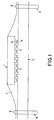
- Figure 1 is a schematic diagram of a solder interconnection pursuant to the present invention.
- FIG. 2 illustrates glass transition temperature (Tg) of the cyanate blends pursuant to the present invention.
- numeral 1 represents a semiconductor chip joined on the chip carrier 2 by solder bumps 3 mated to pads 4.
- I/O pins 5 extend and protrude from the carrier 2, with a small portion 6 of the pins protruding from the other side of the carrier for carrying current thereto.
- the carrier is an organic substrate, the pins (6) as such are not required. Instead, electrically conductive circuitry and interconnections would be provided such as at the periphery of substrate for connection to a desired structure.
- the sealant or encapsulant 7 pursuant to the present invention provides for essentially void free encapsulation of the solder connections thereby assuring highly reliable devices and fills the gap forming a uniform fillet around the chip as well as covering the pin heads under the device (not shown).
- the triazine polymers of the present invention that are suitable for providing the sealant are reaction products of (a) monocyanate; and (b) dicyanate and/or prepolymers thereof.
- the monocyanate is a monomeric monofunctional cyanate and include monocyanates represented by the following formula: NCO-B wherein B represents an alkyl group; alkyl substituted phenyl ring; or a moiety of the formula: wherein A represents a single bond, -S02- -0-, -C(CF3)2, divalent alkylene radicals such as -CH2- and - C(CH3)2-; divalent alkylene radicals interrupted by heteroatoms in the chain such as 0, S and N.
- Each R is independently selected from the group of hydrogen, and alkyl containing 1 to 9 carbon atoms.
- Each n is independently an integer of 0 to 5.
- Suitable alkyl groups for B and for substitution on a phenyl ring typically contain 1 to 16 carbon atoms, and preferably 1 to 9 carbon atoms.
- Suitable monocyanates are nonylphenyl cyanate; dinonyl phenyl cyanate, cumyl phenyl cyanate; phenyl cyanate, 2-,3-, or 4-methyl-, ethyl-, n-propyl-, isopropyl-, n-butyl-, isobutyl-, tert-butyl-, n- or iso-pentyl-, n or isohexyl-, n-or isoheptyl-, n-or isooctyl-, n- or isononyl-, n- or isodecyl-, ethene-, propene-, butane- and ethinphenylcyanate, 2,3-, 2,4-, 2,5-, 2,6-, 3,4-, 3,5- dimethyl-, diethyl-, dipropylphenylcyanates; 2,3,4-, 2,3,5-,
- cycloalkylphenyl cyanates for instance 2-, 3- or 4- cyclohexylphenylcyanate, substituted alkylphenyl cyanates, for instance 4-chloromethyl, 4-hydroxy methyl-, and 3-trifluoromethylphenyl cyanate; aralkylphenylcyanates, for instance 2-, 3- or 4-phenylcyanates, halogenophenyl cyanates, for instance 2-, 3-, or 4-chloro- or bromophenylcyanate, 2,3-, 2,4-, 2,5-, 2,6-, 3,4-, 3,5-dichloro (bromo)-phenyl cyanate, 2-methyl-5-chloro-, 2-methyl-6-chloro, 3-methyl-4-chloro-, 5-methyl-2-chloro-, 2-methyl-4-chloro-, 2 methyl-3-chlorophenylcyanate, nitrophenyl cyanates, alkyloxy, aryloxy-, acyl
- the monocyanates can be prepared from the corresponding phenol analogs by reacting with a cyanogen halide such as cyanogen bromide in the presence of base catalyst such as triethylamine.
- a cyanogen halide such as cyanogen bromide
- base catalyst such as triethylamine
- the dicyanate esters are curable through cyclotrimerization and can be monomeric or less desirably prepolymers, including oligomers and can be represented by those materials containing the following formula: wherein A represents independently a single bond, -CH2OCH2-, -S-, - S02 -, - 0 -, -C(CF3)2-, divalent alkylene radicals such as - CH2- and -C(CH3)2-; divalent alkylene radicals interrupted by heteroatoms in the chain such as O, S and N.
- Each R is independently selected from the group of hydrogen, alkyl containing 1 to 9 carbon atoms:
- n independently is an integer of 0 to 4.
- Other polyfunctional cyanates are prepared by well known methods, for example, by reacting the corresponding polyvalent phenol with a halogenated cyanate as exemplified in U.S. Patent Nos. 3,553,244, 3,740,348 and 3,755,402.
- polyfunctional cyanate ester examples include 1,3- or 1,4-dicyanatobenzene; 1,3,5-tricyanatobenzene; 1,3-, 1,4-, 1,6-, 1,8-, 2,6-, or 2,7-dicyanatonaphthalene; 1,3,6-tricyanatonaphthalene; 4,4'-dicyanatonaphthalene; bis(4-cyanatophenyl) propane, 2,2-bis(3,5-dichloro-4-cyanatophenyl)propane; bis(4-cyanatophenyl) ether; bis(4-cyanatophenyl)thioethers, bis(4-cyanatophenyl) sulfone; tris-(4-cyanatophenyl) phosphite; tris(4-cyanatophenyl) phosphate; bis(3-chloro-4-cyanatophenyl) methane; cyanated novolak derived from novolak, cyanated bisphenol type poly
- a suitable polyaromatic cyanate ester containing cycloaliphatic bridging group between aromatic rings is available from Dow Chemical Company under the designation "Dow XU-71787 cyanate".
- Dow Chemical Company under the designation "Dow XU-71787 cyanate”.
- a discussion of such can be found in Bogan, et al., "Unique Polyaromatic Cyanate Ester for Low Dielectric Printer Circuit Boards", Sampe Journal , Vol. 24, No. 6, Nov/Dec 1988.
- a specific polyfunctional cyanate ester is Bisphenol AD dicyanate (d,d'-ethylidene bisphenol dicyanate) available from Ciba-Geigy under the trade designation AROCY L-10.
- the amount of the monocyanate is typically about 5 to about 50%, and preferably about 5 to about 40% and most preferably about 5 to about 30% by weight of the total of the monocyanate and dicyanate and/or prepolymer thereof.
- the amount of the dicyanate and/or prepolymer thereof is correspondingly about 50 to about 95% by weight, preferably about 60 to about 95% by weight, and most preferably about 95 to about 70% by weight of the total of the monocyanate and dicyanate and/or prepolymers thereof.
- compositions of the present invention can also include a filler and especially an inorganic filler.
- the particular size of the filler is typically not greater than about 49 microns or less, preferably about 0.7 to about 40 microns. This is desirable so that the compositions will have the desired CTE and viscosity characteristics and readily flow in the gap between the chip and substrate carrier.
- the gap is normally about 25 to about 160 microns and preferably about 75 to about 125 microns.
- the preferred fillers have average particle size of about 5 to about 25 microns.
- the filler should be at least substantially free of alpha particular emissions such as from the trace amounts of radioactive impurities such as uranium and thorium normally present in conventional silica or quartz fillers.
- the fillers employed have emission rates of less than 0.01 alpha particles/cm2-hr and preferably less 0.005 alpha particles/cm2-hr.
- the presence of alpha particle emissions primarily caused by the presence of uranium and thorium isotopes in the fillers can generate electron/hole pairs which in turn would be detrimental to the device.
- the preferred filler is high purity fused or amorphous silica.
- a commercially available filler that can be employed is DP4910 from PQ Corporation.
- the preferred filler can be optionally treated with a coupling agent.
- compositions of the present invention contains about 30 to about 50% by weight and preferably about 40% by weight of the binder and correspondingly about 70% to about 50% by weight and preferably about 55% by weight of the filler. These amounts are based upon the total amounts of binder and filler in the composition.
- the compositions can also include a catalyst to promote the polymerization of the cyanate ester mixture.
- Suitable catalysts for the cyanate ester include Lewis acids, such as aluminum chloride, boron trifluoride, ferric chloride, titanium chloride, and zinc chloride; salts of weak acids, such as sodium acetate, sodium cyanide, sodium cyanate, potassium thiocyanate, sodium bicarbonate, and sodium boronate.
- Preferred catalysts are metal carboxylates and metal chelates, such as cobalt, iron, zinc, manganese and copper acetylacetonate or octoates or naphthenates.
- the amount of catalyst when used can vary, and generally will be 0.005 to 5 weight percent, preferably 0.05 to 0.5 weight percent based on total solid binder weight.
- Surfactants in amounts of about 0.5% to about 3% and preferably about 1% to about 1.4% can be used to facilitate flow of the compositions.
- Suitable surfactants include silanes and non-ionic type surface active agents.
- non-ionic alkylphenyl polyether alcohols including those available under the trade designation Triton from Rohm & Haas Co.
- These surface active agents are prepared by the reaction of octylphenol or nonylphenol with ethylene oxide and have the following general structural formula, respectively: in which the alkyl group is a mixture of branched-chain isomers and x is the average number of ethylene oxide units in the ether side chain.
- compositions of the present invention also include an organic dye in amounts less than about 0.2% to provide contrast.
- Suitable dyes are nigrosine and Orasol blue GN.
- compositions of the present invention are substantially free (e.g. - less than 0.2% by weight) if not completely free from non-reactive organic solvents.
- compositions employed pursuant to the present invention have viscosity at 25°C (Brookfield cone & plate Spindle 51, 20 RPM or equivalent) of about 2,000 to about 30,000 centipoise and preferably about 2,000 to about 20,000 centipoise.
- the compositions can be cured at temperatures of about 180°C to about 200°C in about 1 to about 2 hours and preferably about 1.5 hours.
- the compositions when cured have alpha particle emissions of less than about 0.005 preferably less than about 0.004 counts/cm2-hr and most preferably less than about 0.002 counts/cm2-hr.
- the cured compositions also have coefficient of thermal expansion of about 24 ppm/C to about 38 ppm/°C, glass transition temperature of greater than about 125°C and preferably about 140°C to about 200°C.
- the cured compositions have Shore D hardness of greater than 90, modulus of elasticity at 25°C of greater than 6.895 x 10⁹ N/m2 (1.0 Mpsi) and preferably greater than 8.274 x 10⁹ N/m2 (1.2 Mpsi).
- compositions are prepared by rapidly admixing the components under vacuum usually about 5 mm Hg either using a double planetary mixer or high shear mixer under vacuum to provide better and homogenous compositions.
- composition is applied by dispensing through nozzles under pressure of about 1.379 x 10⁵ to about 6.895 x 10⁶ N/m2 (about 20 to about 50 psi) and temperatures of about 40°C to about 80°C.
- the compositions completely cover the C4 connections and pin heads.
- the substrates be at a temperature of about 65°C to about 100°C during the dispensing.
- compositions are then cured by heating to about 150°C to about 200°C for about 1 hour to about 3 hours and preferably about 1.5 hours to about 2.0 hours.
- the substrate employed can be an organic, inorganic or composite in nature.
- the preferred substrate can be a ceramic module or a multilayer printed circuit board.
- the preferred ceramic substrates include silicon oxides and silicates such as aluminum silicate, and aluminum oxides.
- the organic substrates can be thermoplastic as well as thermosetting polymeric materials.
- the preferred printed circuit board includes conventional FR-4 epoxy and laminates based on high temperature resins such as high temperature epoxies, polyimides, cyanates (trizines), fluoropolymers, benzocyclobutenes, polyphenylenesulfide, polysulfones, polyetherimides, polyetherketones, polyphenylquinoxalines, polybenzoxazoles, and polyphenyl benzobisthiazoles.
- high temperature resins such as high temperature epoxies, polyimides, cyanates (trizines), fluoropolymers, benzocyclobutenes, polyphenylenesulfide, polysulfones, polyetherimides, polyetherketones, polyphenylquinoxalines, polybenzoxazoles, and polyphenyl benzobisthiazoles.
- the polymers can be reinforced such as with glass, for instance epoxy-glass substrates.
- the substrates can be rigid or flexible. Suitable flexible substrates include the flexible polyimide substrates.
- Dinonyl phenol-flashed is obtained from Texaco Chemical Company. It is a viscous liquid possessing a slight phenolic odor and is a mixture of dinonyl phenols, predominantly orthopara-substituted. The nonyl groups are randomly branched. It is used in the synthesis of the cyanate ester with no further purification.
- Distilled water (about 30 ml) and bromine (about 22 g) are introduced into a 500 ml three necked round-bottom flask equipped with a low temperature thermometer, mechanical stirrer, and a 100 ml pressure equalizing dropping funnel. The mixture is stirred rapidly and cooled to -5°C in an ice-salt bath. Sodium cyanide (about 6.5 g) in water (about 30 ml) is then added drop-wise over a period of 30 min; the temperature is maintained below about 5°C during the addition.
- Nonyl phenyl cyanate and p-cumyl phenyl cyanate are prepared from the corresponding phenol analogs according to the procedure described in example 1.
- the Arocy L-10 monomer is obtained from Hi-Tek Polymers, Inc. as a liquid with a purity greater than 99.95%. Blends of Arocy L-10, containing up to 40 percent monocyanate i.e. (dinonyl phenol cyanate, nonyl phenyl or p-cumyl phenyl cyanate) are dissolved by simply mixing the two monomers in the appropriate amounts. The resulting mixtures are catalyzed with zinc octoate (100 ppm zinc metal). Zinc octoate is obtained from Mooney Chemicals, Cleveland, Ohio 44113 as an 8% (zinc metal) solution in mineral spirits.
- the glass transition temperature of each blend is determined using a DuPont 912 dual sample DSC, coupled to the 9900 Thermal Analyzer.
- the instrument is purged with nitrogen at a flow rate of less than 50cc/min during each run.
- the sample size is approximately 8 mg and the heating rate is about 20C/minute. Results are graphically presented in Figure 2.
- the composition is dispensed at a temperature of about 50°C in the gap of about 125 ⁇ m (about 5 mils) between a silicon chip soldered by solder bumps to 28 mm by 28 mm Al203 substrate having pins protruding therefrom.
- the composition is cured at about 180°C in about 2 hours.
- the composition has a coefficient of thermal expansion of less than 28 x 10 ⁇ 6/°C.
- test vehicles filled with prior art compositions show failures at about 2,000 cycles.
- the composition is dispensed at a temperature of about 30°C in the gap of about about 125 ⁇ m (about 5 mils) between a silicon chip soldered by solder pumps to an FR-4 epoxy-glass substrate.
- the mixture covers the solder bumps and forms a fillet around the device.
- the composition is cured at about 170°C in about 2 hours.
- the composition has a coefficient of thermal expansion of less than 30 x 10 ⁇ 6/°C.
- the composition is dispensed at a temperature of about 60°C in the gap of about 125 ⁇ m (about 5 mils) between a silicon device flip-chip bonded to a high Tq epoxy-glass substrate.
- the composition is cured at 170C in about 2 hours and forms a fillet around the silicon chip, on all four sides.
- the composition has a coefficient of thermal expansion of less than 28 x 10 ⁇ 6/°C.
Landscapes
- Chemical & Material Sciences (AREA)
- Health & Medical Sciences (AREA)
- Chemical Kinetics & Catalysis (AREA)
- Medicinal Chemistry (AREA)
- Polymers & Plastics (AREA)
- Organic Chemistry (AREA)
- Macromolecular Compounds Obtained By Forming Nitrogen-Containing Linkages In General (AREA)
- Compositions Of Macromolecular Compounds (AREA)
- Non-Metallic Protective Coatings For Printed Circuits (AREA)
- Manufacturing Of Printed Wiring (AREA)
- Wire Bonding (AREA)
Applications Claiming Priority (2)
| Application Number | Priority Date | Filing Date | Title |
|---|---|---|---|
| US99796492A | 1992-12-29 | 1992-12-29 | |
| US997964 | 1992-12-29 |
Publications (1)
| Publication Number | Publication Date |
|---|---|
| EP0604823A1 true EP0604823A1 (de) | 1994-07-06 |
Family
ID=25544608
Family Applications (1)
| Application Number | Title | Priority Date | Filing Date |
|---|---|---|---|
| EP93120133A Withdrawn EP0604823A1 (de) | 1992-12-29 | 1993-12-14 | Triazinepolymer und Verwendung |
Country Status (3)
| Country | Link |
|---|---|
| US (3) | US5468790A (de) |
| EP (1) | EP0604823A1 (de) |
| JP (1) | JPH06228308A (de) |
Cited By (1)
| Publication number | Priority date | Publication date | Assignee | Title |
|---|---|---|---|---|
| US9169356B2 (en) | 2005-10-25 | 2015-10-27 | Mitsubishi Gas Chemical Company, Inc. | Cyanate ester polymer |
Families Citing this family (26)
| Publication number | Priority date | Publication date | Assignee | Title |
|---|---|---|---|---|
| US5656862A (en) * | 1990-03-14 | 1997-08-12 | International Business Machines Corporation | Solder interconnection structure |
| US5660920A (en) * | 1995-07-14 | 1997-08-26 | The United States Of America As Represented By The Secretary Of The Navy | Inter-level dielectrics with low dielectric constants |
| US5804881A (en) * | 1995-11-27 | 1998-09-08 | Motorola, Inc. | Method and assembly for providing improved underchip encapsulation |
| US5880530A (en) * | 1996-03-29 | 1999-03-09 | Intel Corporation | Multiregion solder interconnection structure |
| US5948922A (en) * | 1997-02-20 | 1999-09-07 | Cornell Research Foundation, Inc. | Compounds with substituted cyclic hydrocarbon moieties linked by secondary or tertiary oxycarbonyl containing moiety providing reworkable cured thermosets |
| US5981312A (en) * | 1997-06-27 | 1999-11-09 | International Business Machines Corporation | Method for injection molded flip chip encapsulation |
| DE69807793T2 (de) * | 1997-07-04 | 2003-08-14 | Hitachi Chemical Co., Ltd. | Mit einem Cyanatester modifizierte härtbare Harzzusammensetzung und daraus hergestellter Lack, Prepreg, mit Metall bedeckte Schichtplatte, Film, gedruckte Leiterplatte und Mehrschichtleiterplatte |
| US6245841B1 (en) * | 1998-03-23 | 2001-06-12 | General Electric Company | Cyanate ester based thermoset compositions |
| US6162876A (en) * | 1998-03-23 | 2000-12-19 | General Electric Company | Cyanate ester based thermoset compositions |
| US6194495B1 (en) * | 1998-03-23 | 2001-02-27 | General Electric Company | Cyanate ester based thermoset compositions |
| US6569710B1 (en) * | 1998-12-03 | 2003-05-27 | International Business Machines Corporation | Panel structure with plurality of chip compartments for providing high volume of chip modules |
| US6455354B1 (en) | 1998-12-30 | 2002-09-24 | Micron Technology, Inc. | Method of fabricating tape attachment chip-on-board assemblies |
| US20020030257A1 (en) | 1999-06-18 | 2002-03-14 | Joseph M. Brand | Semiconductor device utiling an encapsulant for locking a semiconductor die to circuit substrate |
| EP1067149A1 (de) * | 1999-07-01 | 2001-01-10 | Fraunhofer-Gesellschaft zur Förderung der angewandten Forschung e.V. | Polycyanatcopolymere aus polyfunktionellen Cyanaten und fluorierten Monocyanaten |
| JP2003060341A (ja) * | 2001-08-08 | 2003-02-28 | Mitsubishi Gas Chem Co Inc | 細密パターンを有するプリント配線板の製造方法。 |
| JP2003069218A (ja) * | 2001-08-23 | 2003-03-07 | Mitsubishi Gas Chem Co Inc | 極細線パターンを有するプリント配線板の製造方法 |
| US7047633B2 (en) * | 2003-05-23 | 2006-05-23 | National Starch And Chemical Investment Holding, Corporation | Method of using pre-applied underfill encapsulant |
| JP4451214B2 (ja) * | 2004-05-21 | 2010-04-14 | シャープ株式会社 | 半導体装置 |
| DE102004039693B4 (de) * | 2004-08-16 | 2009-06-10 | Infineon Technologies Ag | Vergussmasse, Chipmodul und Verfahren zur Herstellung eines Chipmoduls |
| US20060046321A1 (en) * | 2004-08-27 | 2006-03-02 | Hewlett-Packard Development Company, L.P. | Underfill injection mold |
| JP2007059767A (ja) * | 2005-08-26 | 2007-03-08 | Shinko Electric Ind Co Ltd | アンダーフィル材を用いて電子部品を搭載した基板及びその製造方法 |
| JP5486890B2 (ja) * | 2009-09-30 | 2014-05-07 | ミネベア株式会社 | ファンモータ |
| KR101892784B1 (ko) | 2011-08-09 | 2018-08-28 | 미츠비시 가스 가가쿠 가부시키가이샤 | 신규한 시안산에스테르 화합물 및 그 제조 방법, 그리고 그 화합물을 함유하는 경화성 수지 조성물 및 그 경화물 |
| JP5892871B2 (ja) * | 2011-11-22 | 2016-03-23 | 株式会社日立製作所 | トリアジン環を含有する有機‐無機複合材料及びそれを用いた電気的装置 |
| JPWO2013084819A1 (ja) | 2011-12-07 | 2015-04-27 | 三菱瓦斯化学株式会社 | 樹脂組成物、プリプレグ及び積層板 |
| WO2013115069A1 (ja) * | 2012-01-31 | 2013-08-08 | 三菱瓦斯化学株式会社 | プリント配線板材料用樹脂組成物、並びにそれを用いたプリプレグ、樹脂シート、金属箔張積層板及びプリント配線板 |
Citations (2)
| Publication number | Priority date | Publication date | Assignee | Title |
|---|---|---|---|---|
| US4604644A (en) * | 1985-01-28 | 1986-08-05 | International Business Machines Corporation | Solder interconnection structure for joining semiconductor devices to substrates that have improved fatigue life, and process for making |
| WO1989006647A1 (en) * | 1988-01-22 | 1989-07-27 | The Dow Chemical Company | Aromatic polycyanate/monocyanate comonomer compositions and polytriazines derived therefrom |
Family Cites Families (27)
| Publication number | Priority date | Publication date | Assignee | Title |
|---|---|---|---|---|
| CA775188A (en) * | 1968-01-02 | Berndt Gerhard | Stabilization of ester-containing synthetic resins | |
| NL277028A (de) * | 1961-04-19 | |||
| IT1052501B (it) * | 1975-12-04 | 1981-07-20 | Chimosa Chimica Organica Spa | Composti politriazinici utilizzabili per la stabilizzazione di polimeri sintetici e procedimento per la loro preparazione |
| US4180404A (en) * | 1977-11-17 | 1979-12-25 | Asahi Kasei Kogyo Kabushiki Kaisha | Heat resistant photoresist composition and process for preparing the same |
| JPS555537A (en) * | 1978-06-28 | 1980-01-16 | Masaki Yoshimura | Transmitter of spectrum diffusion |
| JPS57143320A (en) * | 1981-02-28 | 1982-09-04 | Mitsubishi Gas Chem Co Inc | Novel curable resin composition |
| US4690962A (en) * | 1982-05-24 | 1987-09-01 | International Business Machines Corporation | Composition, coated article and method of coating |
| US4456712A (en) * | 1982-06-14 | 1984-06-26 | International Business Machines Corporation | Bismaleimide triazine composition |
| US4623577A (en) * | 1985-02-01 | 1986-11-18 | Allied Corporation | Circuit board made from cross-linked polycyanurate polymer, thermoplastic polymer and polyaramid fiber |
| DE3516089A1 (de) * | 1985-05-04 | 1986-11-06 | Bayer Ag, 5090 Leverkusen | Mit monoisocyanaten modifizierte polyamide |
| US4776904A (en) * | 1985-07-19 | 1988-10-11 | Miles Inc. | Multilayer analytical element and method of making, using ultrasonic or laser energy |
| US4632577A (en) * | 1985-09-16 | 1986-12-30 | Ncr Corporation | Record media thickness compensating mechanism |
| US4742118A (en) * | 1986-05-16 | 1988-05-03 | American Cyanamid Company | Urethane-functional s-triazine crosslinking agents and curable compositions containing the same |
| US4745215A (en) * | 1987-04-03 | 1988-05-17 | International Business Machines Corporation | Fluorine containing dicyanate resins |
| US5015719A (en) * | 1987-04-03 | 1991-05-14 | International Business Machines Corporation | Aromatic dicyanate/aromatic diepoxy compositions, cured products and methods |
| CA1335077C (en) * | 1988-02-08 | 1995-04-04 | Henri Isliker | Process for the manufacture of apolipoproteins from human blood plasma or serum |
| JP2978511B2 (ja) * | 1989-09-20 | 1999-11-15 | 株式会社日立製作所 | 集積回路素子実装構造体 |
| EP0441047B1 (de) * | 1990-01-19 | 1996-06-05 | Minnesota Mining And Manufacturing Company | Wärmehärtbare Zusammensetzung |
| US4999699A (en) * | 1990-03-14 | 1991-03-12 | International Business Machines Corporation | Solder interconnection structure and process for making |
| US5121190A (en) * | 1990-03-14 | 1992-06-09 | International Business Machines Corp. | Solder interconnection structure on organic substrates |
| US5089440A (en) * | 1990-03-14 | 1992-02-18 | International Business Machines Corporation | Solder interconnection structure and process for making |
| JP2503003Y2 (ja) * | 1990-03-30 | 1996-06-26 | 株式会社東富士製作所 | 線材カット用ナイフ |
| US5065227A (en) * | 1990-06-04 | 1991-11-12 | International Business Machines Corporation | Integrated circuit packaging using flexible substrate |
| US5194930A (en) * | 1991-09-16 | 1993-03-16 | International Business Machines | Dielectric composition and solder interconnection structure for its use |
| US5167674A (en) * | 1992-04-13 | 1992-12-01 | Norton Company | Bismaleimide-triazine resin bonded superabrasive wheels |
| US5312887A (en) * | 1992-12-09 | 1994-05-17 | International Business Machines Corporation | Dicyanate prepolymers, use and preparation thereof |
| US5292861A (en) * | 1992-12-29 | 1994-03-08 | International Business Machines Corporation | Trifunctional cyanate esters, polymers thereof; use and preparation thereof |
-
1993
- 1993-12-14 JP JP5312989A patent/JPH06228308A/ja active Pending
- 1993-12-14 EP EP93120133A patent/EP0604823A1/de not_active Withdrawn
-
1994
- 1994-09-13 US US08/304,826 patent/US5468790A/en not_active Expired - Fee Related
-
1995
- 1995-06-06 US US08/466,716 patent/US5623006A/en not_active Expired - Fee Related
- 1995-06-06 US US08/466,366 patent/US5536765A/en not_active Expired - Fee Related
Patent Citations (3)
| Publication number | Priority date | Publication date | Assignee | Title |
|---|---|---|---|---|
| US4604644A (en) * | 1985-01-28 | 1986-08-05 | International Business Machines Corporation | Solder interconnection structure for joining semiconductor devices to substrates that have improved fatigue life, and process for making |
| EP0189791A2 (de) * | 1985-01-28 | 1986-08-06 | International Business Machines Corporation | Lotverbindungsstruktur zum Verbinden von Halbleiteranordnungen mit Substraten und Verfahren zur Herstellung derselben |
| WO1989006647A1 (en) * | 1988-01-22 | 1989-07-27 | The Dow Chemical Company | Aromatic polycyanate/monocyanate comonomer compositions and polytriazines derived therefrom |
Non-Patent Citations (1)
| Title |
|---|
| SPAULDING ET AL.: "Coating material", IBM TECHNICAL DISCLOSURE BULLETIN, vol. 13, no. 4, September 1970 (1970-09-01), NEW YORK US, pages 825 * |
Cited By (1)
| Publication number | Priority date | Publication date | Assignee | Title |
|---|---|---|---|---|
| US9169356B2 (en) | 2005-10-25 | 2015-10-27 | Mitsubishi Gas Chemical Company, Inc. | Cyanate ester polymer |
Also Published As
| Publication number | Publication date |
|---|---|
| US5623006A (en) | 1997-04-22 |
| JPH06228308A (ja) | 1994-08-16 |
| US5536765A (en) | 1996-07-16 |
| US5468790A (en) | 1995-11-21 |
Similar Documents
| Publication | Publication Date | Title |
|---|---|---|
| US5536765A (en) | Method of sealing a soldered joint between a semiconductor device and a substrate | |
| US5250848A (en) | Solder interconnection structure | |
| US4999699A (en) | Solder interconnection structure and process for making | |
| US5656862A (en) | Solder interconnection structure | |
| US5121190A (en) | Solder interconnection structure on organic substrates | |
| JP2539996B2 (ja) | はんだ相互接続構造体、及び組成物 | |
| US7384682B2 (en) | Electronic package with epoxy or cyanate ester resin encapsulant | |
| EP1299447B1 (de) | Nichtfliessende flussmittel-klebstoffzusammensetzungen | |
| KR101265988B1 (ko) | 플럭싱용 조성물 | |
| CA2083514A1 (en) | Reworkable adhesive for electronic applications | |
| US6172143B1 (en) | Resin composition for use in sealant and liquid sealant using the resin composition | |
| JP2001506313A (ja) | アンダーフィル密封材として有用な熱硬化性樹脂組成物 | |
| KR101553102B1 (ko) | 열경화성 수지 조성물을 포함하는 반도체 장치의 신뢰성을 향상시키는 방법 | |
| EP0528171B1 (de) | Masse, die eine Mischung von Dicyanaten enthält, und ihre Verwendung | |
| US6492438B1 (en) | Electrically connectable adhesive agent for semiconductor | |
| US6469074B1 (en) | Composition of cyanate ester, epoxy resin and acid anhydride | |
| US20040086719A1 (en) | Organic acid containing compositions and methods for use thereof | |
| JP2003002949A (ja) | 半導体封止用液状エポキシ樹脂組成物および半導体装置 | |
| JP2003147321A (ja) | 接着剤 | |
| JP2000336246A (ja) | 半導体封止用液状エポキシ樹脂組成物および半導体装置 | |
| JP2000336245A (ja) | 半導体封止用液状エポキシ樹脂組成物および半導体装置 |
Legal Events
| Date | Code | Title | Description |
|---|---|---|---|
| PUAI | Public reference made under article 153(3) epc to a published international application that has entered the european phase |
Free format text: ORIGINAL CODE: 0009012 |
|
| AK | Designated contracting states |
Kind code of ref document: A1 Designated state(s): DE FR GB |
|
| 17P | Request for examination filed |
Effective date: 19941021 |
|
| 17Q | First examination report despatched |
Effective date: 19960222 |
|
| STAA | Information on the status of an ep patent application or granted ep patent |
Free format text: STATUS: THE APPLICATION IS DEEMED TO BE WITHDRAWN |
|
| 18D | Application deemed to be withdrawn |
Effective date: 19970311 |