EP0446855B1 - Multikanal-Kommunikationsverarbeitungssystem - Google Patents
Multikanal-Kommunikationsverarbeitungssystem Download PDFInfo
- Publication number
- EP0446855B1 EP0446855B1 EP19910103730 EP91103730A EP0446855B1 EP 0446855 B1 EP0446855 B1 EP 0446855B1 EP 19910103730 EP19910103730 EP 19910103730 EP 91103730 A EP91103730 A EP 91103730A EP 0446855 B1 EP0446855 B1 EP 0446855B1
- Authority
- EP
- European Patent Office
- Prior art keywords
- data
- line
- transmitting
- receiving
- control means
- Prior art date
- Legal status (The legal status is an assumption and is not a legal conclusion. Google has not performed a legal analysis and makes no representation as to the accuracy of the status listed.)
- Expired - Lifetime
Links
- 230000006854 communication Effects 0.000 title claims description 53
- 238000004891 communication Methods 0.000 title claims description 51
- 230000015654 memory Effects 0.000 claims description 42
- 239000000872 buffer Substances 0.000 claims description 9
- 239000004065 semiconductor Substances 0.000 claims description 6
- 230000000694 effects Effects 0.000 claims description 4
- 238000000034 method Methods 0.000 description 13
- 238000010586 diagram Methods 0.000 description 9
- 239000000758 substrate Substances 0.000 description 4
- 230000005540 biological transmission Effects 0.000 description 3
- 238000005516 engineering process Methods 0.000 description 3
- XUIMIQQOPSSXEZ-UHFFFAOYSA-N Silicon Chemical compound [Si] XUIMIQQOPSSXEZ-UHFFFAOYSA-N 0.000 description 2
- 230000006870 function Effects 0.000 description 2
- 230000010354 integration Effects 0.000 description 2
- 229910052710 silicon Inorganic materials 0.000 description 2
- 239000010703 silicon Substances 0.000 description 2
- 238000003860 storage Methods 0.000 description 2
- 230000003139 buffering effect Effects 0.000 description 1
- 238000010276 construction Methods 0.000 description 1
- 238000009434 installation Methods 0.000 description 1
- 238000004519 manufacturing process Methods 0.000 description 1
- 238000013341 scale-up Methods 0.000 description 1
Images


Classifications
-
- H—ELECTRICITY
- H04—ELECTRIC COMMUNICATION TECHNIQUE
- H04L—TRANSMISSION OF DIGITAL INFORMATION, e.g. TELEGRAPHIC COMMUNICATION
- H04L12/00—Data switching networks
- H04L12/54—Store-and-forward switching systems
- H04L12/56—Packet switching systems
-
- H—ELECTRICITY
- H04—ELECTRIC COMMUNICATION TECHNIQUE
- H04L—TRANSMISSION OF DIGITAL INFORMATION, e.g. TELEGRAPHIC COMMUNICATION
- H04L69/00—Network arrangements, protocols or services independent of the application payload and not provided for in the other groups of this subclass
- H04L69/14—Multichannel or multilink protocols
-
- H—ELECTRICITY
- H04—ELECTRIC COMMUNICATION TECHNIQUE
- H04Q—SELECTING
- H04Q11/00—Selecting arrangements for multiplex systems
- H04Q11/04—Selecting arrangements for multiplex systems for time-division multiplexing
- H04Q11/0428—Integrated services digital network, i.e. systems for transmission of different types of digitised signals, e.g. speech, data, telecentral, television signals
Definitions
- the present invention relates to a communication processing system for controlling a data transfer to a plurality of lines in accordance with a communication protocol.
- FIG. 2 illustrates a construction of this conventional system.
- a communication processing system 2 comprises a line control module 21, a transmitting/receiving FIFO (first-in first-out) memory 22, a DMA (direct memory access) control module 23, a memory 24, a CPU (central processing unit) 25 and an internal bus 26.
- the line control module 21 effects a serial interface with a remote station through transmitting/receiving lines.
- the memory 22 temporarily stores the transmitting/receiving data.
- the DMA control module 23 transfers the data directly to a main memory 3 on the side of a host processor 4.
- the memory 24 stores a communication processing program and the data.
- the CPU 25 controls the communication processing system 2 as a whole.
- the bus 26 connects circuits of the system 2.
- the communication processing system 2 is formed on a single semiconductor substrate such as a silicon substrate by a known semiconductor integrated circuit processing technology to provide LSI (large-scale integration).
- the communication processing system LSI 2 is employed for processing a link access procedure on D-channel (LAPD) serving as a communication protocol of, e.g., anintegrated services digital network (ISDN).
- LAPD link access procedure on D-channel
- ISDN integrated services digital network
- a transmitting/receiving line rate is 16 or 64 kbps
- an operating system clock of the internal CPU 25 is, for instance, 6 MHz.
- the conventional technology described above is limited to a case where only one transmitting/receiving line is prepared. No consideration is given to an application to a system having a plurality of lines.
- the communication processing systems LSI 2 be used one by one for every line. This results in a scale-up of the whole system and an increase in costs as well.
- the transmitting/receiving line rate of 16 kbps or 64 kbps is approximately 1/100, a very low speed as compared with the operating system clock of 6 MHz of the built-in CPU 25.
- the time for waiting for an interruption from the line control module 21 or the DMA control module 23 is much longer than in a state where the built-in CPU 25 works to control the single transmitting/ receiving line.
- the communication processing system LSI 2 is therefore inefficient.
- EP-A-0 259 117 discloses a communication processing system with the features included in the first part of claim 1, specifically a distributed packet switching system including a number of switching modules each having a plurality of access ports. Incoming and outgoing packet channels are extended between each switching module and an inter-module packet switch. Each switching module transmits user information packets, via an incoming or outgoing packet channel, between the access ports and the inter-module packet switch.
- the invention meets this object by providing a communication processing system as defined in claim 1.
- a multiplex control circuit for effecting an interface between a multiplex transmitting/receiving line and said line correspondence units, said multiplex control circuit separating multiplexed data transmitted from said multiplex transmitting/receiving line, supplying the data to said line correspondence units, multiplexing en bloc the data supplied from said line correspondence units and sending the multiplex data to said multiplex transmitting/receiving line.
- the data transferred between the CPU, the line control means, the DMA control means and the memory may contain channel information.
- the multichannel communication processing system can be constructed of one or a plurality of semiconductor chips.
- the multichannel communication processing system of this invention is applicable to an ISDN communication protocol LSI and an exchange.
- the low-speed data when receiving the data from the lines, the low-speed data are temporarily stored in the respective line correspondence units. The data are then transferred via the line control module to the CPU.
- the CPU is capable of processing at a high speed with the aid of the line control module and the DMA control module. The CPU therefore can execute the receiving process of a plurality of low-speed data lines.
- the CPU transmits the transmitting data distributively to the line correspondence units at the high speed with the aid of the DMA control module and the line control module.
- the line correspondence units in turn transmit the data to the external lines at a low speed.
- the communication process can be executed at a high efficiency on the occasion of transmitting/receiving data on the plurality of lines.
- the whole system can be miniaturized.
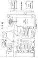
- FIG. 1 is a block diagram illustrating a configuration of one embodiment of a multichannel communication processing system including a transform-into-multichannel means.
- a multichannel communication processing system 1 is constructed on one semiconductor substrate such as a silicon substrate by a known semiconductor integrated circuit technology.
- the communication processing system LSI 1 is connected to a system bus 5 together with a main memory 3 for storing transmitting/receiving data and a variety of parameters for communication protocol processing. A predetermined communication function module is thus configured.
- the communication processing system LSI 1 supports data transfer control procedures and other control when effecting data communications with other communication function modules in which a host processor 4 serves as a remote station.
- the communication processing system LSI 1 comprises a plurality of line correspondence units 61 - 68, a channel selector 7, a line control circuit 8, status registers 81 - 88 provided per line and concomitant therewith, a DMA control circuit 9, parameter registers 91 - 98 provided per channel and concomitant therewith, a CPU 10, a memory module 11 and a common internal bus 12.
- the line correspondence units 61 - 68 perform serial interfaces with the remote station via a receiving line RL and a transmitting line TL.
- the line control circuit 8 analyzes a receiving frame via any one of the line correspondence units 61 - 68.
- the DMA control circuit 9 transfers the data not via the host processor 4 but directly to the main memory 3.
- the CPU 10 controls the communication processing system LSI 1 as a whole.
- the memory module 11 is constructed of: a RAM for rewritably storing various control data such as system constants needed for controlling the data transfer and also various control information necessary for controlling the data transfer under DMA control; and a ROM into which a communication protocol processing program for prescribing the communication processing procedures and other programs for controlling the entire communication processing system 1 are incorporated.
- the common internal bus 12 serves to connect circuits of the system 1. Note that the number 8 of the line correspondence units 61 - 68 is a mere example; other numbers are possible.
- the channel selector 7, the line control circuit 8 and the status registers 81 - 88 provided per channel are combined to constitute a line control means A.
- the DMA control circuit 9 and the parameter registers 91 - 98 provided per channel are combined to form a DMA control means B.
- the line correspondence units 61 - 68 form a line correspondence means C.
- the line correspondence means C is composed of, e.g., an FIFO type data buffer.
- a storage capacity of the data buffer is desirably set so as to be sufficient to effect buffering even when simultaneously receiving all the channels without a back-up memory. The data buffer storage capacity will be explained later in detail with reference to FIG. 6.
- a receiving data bus 13 and a transmitting data bus 14 which are dedicated to transmission and reception can be provided between the DMA control circuit 9 and the line control circuit 8.
- the installation of the receiving/transmitting data buses 13 and 14 dedicated to the transmission and reception makes it possible to evade conflicts with transfers of other data. A data transfer velocity is thereby improved.
- a register file 15 Connectable to the common internal bus 12 separately from the memory module 11 are a register file 15 in which only the register is made independent and a memory interface 16 used for an expansion of the memory module 11.
- the control procedures of a high level data link control (HDLC) system are adopted.
- Received via the receiving line of each channel is a frame in which an address, a control field, an information field and a frame check sequence are interposed between flag sequences.
- the line correspondence units 61 - 68 of the line correspondence means C when receiving the frames, the frames are accumulated in the FIFO type data buffer.
- the line control circuit 8 of the line control means A is informed of the fact that the frames are received.
- the line control circuit 8 receives a signal informing the receipt of frames coming in from the plurality of line correspondence units 61 - 68.
- the CPU 10 is informed of this by, e.g., an interruption system.
- the CPU 10 receives this interruption and reads the control information on channel numbers, channel present statuses, addresses and control fields from the line control circuit 8.
- the CPU 10 checks a variety of parameters stored in the memory module 11. In the case of the frame to be received correctly, a receiving process start command is issued to the DMA control circuit 9 of the DMA control means B as well as to the line control circuit 8. Furthermore, the CPU 10 sets, in the per-channel parameter registers 91 - 98 of the DMA control circuit 9, parameters such as the number of bytes and addresses of the data buffer on the main memory 3 defined as a transfer destination of the information field.
- the line control circuit 8 controls the channel selector 7 on the basis of the channel numbers.
- the information fields of the frames accumulated in the line control circuit 8 are transferred while being marked with the channel numbers via the receiving data bus 13 to the DMA control circuit 9.
- the received data are transferred to a predetermined data buffer of the main memory 3 on the basis of values of the per-channel parameter registers 91 - 98, thus completing the receiving process.
- the CPU 10 when transmitting the frames, the CPU 10 receives a frame transmitting start command from the host processor 4. If proven to be a frame transmittable status at that channel by referring to the memory module 11 and various registers, the CPU 10 issues the transmitting process start command to the DMA control circuit and the line control circuit 8 as well.
- the DMA control circuit 9 reads the data which form the information fields of the frame to be transmitted from the transmitting data buffer of the main memory 3 with reference to the per-channel parameter registers 91 - 98. Such data are transferred via the transmitting data bus 14 to the line control circuit 8.
- the status register of the channel number concerned is updated in accordance with the transmitted data.
- the address, control field and frame check sequence are added for fabricating the frame.
- the frames are sent via the channel selector 7 to the line correspondence units 61 - 68 of the channel numbers designated from the CPU 10.
- the received frames are then transmitted to the transmitting line TL in accordance with line clocks, thus completing a series of transmitting processes.
- this embodiment it is possible to obtain a multichannel communication processing system for executing the communication processes of a plurality of channels, this system including a mere set of the CPU, the line control means A, the DMA control means B, the memory module and the line correspondence means C having the line correspondence units the number of which corresponds to the number of channels.
- this system can be miniaturized on the whole. The costs can remarkably be reduced.
- the number of lines which corresponds to the maximum processing capability of the built-in CPU is freely set.
- the processing capability can be optimized, thereby making it possible to enhance a system efficiency.
- FIG. 3 is a block diagram depicting a configuration of one embodiment of an exchange equipped with a multichannel communication processing system of this invention.
- a private branch exchange 30 is separated into a unit on the side of a station exchange and a unit on the side of an extension terminal, with a time-division multiplex switch 31 serving as its centre.
- the multichannel communication processing system 1 is employed for the extension terminal.
- One multichannel communication system 1 works to process the data of a plurality of, e.g., eight extension lines. Therefore, the entire system of the private branch exchange 30 can be miniaturized, and its manufacturing costs can remarkably be reduced.
- the respective transmitting/receiving lines are independent per channel. Physically, however, a plurality of channels can be time-division-multiplexed by a single transmitting/receiving line.
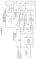
- FIG. 4 is a block diagram showing a configuration of one embodiment of the multichannel communication processing system of this invention, wherein the plurality of channels are time-division-multiplexed by the single transmitting/receiving line.
- FIG. 5 is a time chart showing signals on the transmitting/receiving line and clock waveforms.
- 8-bit data of a channel 1, a channel 2 and a channel 3, ... are time-division-multiplexed. Supplied from outside are a channel clock indicating a channel section and a data clock indicating a bitwise data section.
- a multiplex control circuit 40 multiplexes or separates the data multiplexed on the basis of the channel clock and the data clock. More specifically, the multiplexed and received data are separated and supplied to the line correspondence unit 61. Reversely, the data given from the line correspondence unit 61 are multiplexed en bloc and sent to the multiplex transmitting/receiving line.
- the integration on one chip may be effected together with the multichannel communication processing system 1.
- FIG. 6 is a block diagram illustrating a detailed configuration of one embodiment of the line correspondence unit.
- the line correspondence unit 61 includes: an 8-bit receiving shift register 64 for converting serial receiving data into parallel receiving data; a receiving FIFO memory 66 for temporarily accumulating the receiving data; a transmitting FIFO memory 63 for temporarily accumulating the transmitting data; and a transmitting shift register 65 for converting parallel transmitting data into serial transmitting data.
- the operation of the line correspondence unit 61 will next be described.
- the serial data received at a rate of, e.g., 16 kbps are converted 8-bitwise into parallel data by the receiving shift register 64.
- the parallel data are then stored in a receiving FIFO memory 66.
- the line correspondence unit 61 transmits a signal indicating, e.g., existence of receiving FIFO memory data to the line control circuit 8.
- the same unit 61 then waits for processing by the line control circuit 8.
- the line control circuit 8 sequentially reads the data of the receiving FIFO memory 66 at timings when processing the receiving data of the line correspondence unit of that channel.
- the circuit 8 then executes the necessary process.
- the line correspondence unit 61 transmits, if the transmitting FIFO memory is unoccupied, a signal indicating, e.g., non-existence of transmitting FIFO memory data to the line control circuit 8 at the transmitting time.
- the line control circuit 8 which has received this signal, writes the data to the transmitting FIFO memory 63 when a necessity for transmission arises.
- the transmitting shift register 65 converts the received parallel data into serial data and transmits the data at a rate of, e.g., 16 kbps.
- FIG. 6 shows an example of providing the 5-stage 8-bit receiving FIFO memories 66 and the 5-stage 8-bit transmitting FIFO memories 63. Considerations will herein be given to the number of stages of the FIFO memories required. It is assumed that the number of channels is set to 8, and a load at which receiving of all the channels is simultaneously effected is set at the maximum level.
- the transmitting process is executable at a smaller number of steps than in the receiving process. Therefore, the number of transmitting FIFO memories 63 may be smaller than that of the receiving FIFO memories 66.
- the present invention it is feasible to obtain a multichannel communication processing system consisting of a mere set of the CPU, the line control means, the DMA control means, the memory module and the line correspondence means including the line correspondence units the number of which corresponds to the number of channels, whereby communication processing of the plurality of channels can be executed. Therefore, the entire system can be miniaturized, and the costs are considerably reduced.
- the number of lines which corresponds to the maximum processing capability of the built-in CPU is freely set, and the processing capability can be optimized. As a result, the system efficiency can be enhanced.
Landscapes
- Engineering & Computer Science (AREA)
- Computer Networks & Wireless Communication (AREA)
- Signal Processing (AREA)
- Computer Security & Cryptography (AREA)
- Communication Control (AREA)
- Computer And Data Communications (AREA)
Claims (8)
- Kommunikations-Verarbeitungssystem zur Steuerung einer Datenübertragung an mehrere Leitungen (RL, TL) gemäß einem Kommunikationsprotokoll, wobei das System eine Steuereinrichtung (B) für Speicherdirektzugriff (DMA) zur Übertragung von Daten direkt an einen Hauptspeicher (3), einen Speicher (11) zur Speicherung verschiedener Daten und eines Kommunikationsprotokoll-Verarbeitungsprogramms, eine zentrale Verarbeitungseinheit (CPU 10) zur Gesamtsteuerung des Kommunikations-Verarbeitungssystems sowie eine Leitungsanschlußeinrichtung (C) mit Leitungsanschlußeinheiten (61, 62, 68) als Schnittstellen mit Kanälen der mehreren Leitungen (RL, TL) aufweist,
dadurch gekennzeichnet,
daß das System ferner eine Leitungssteuereinrichtung (A) zur Analyse von Empfangsrahmen und Kanalsteuer-Übertragungsrahmen aufweist, und
daß die Leitungsanschlußeinheiten (61, 62, 68) als Schnittstellen zwischen den Leitungen (RL, TL) und der Leitungssteuereinrichtung (A) dienen,
wobei die Leitungsanschlußeinheiten (61, 62, 68) Datenpuffer (63-66) zur vorübergehenden Speicherung der Daten, die Leitungssteuereinrichtung (A) einen Kanalwähler (7) zum Anwählen der Leitungsanschlußeinheiten (61, 62, 68) sowie Register (81-88) zur Aufnahme von Statusinformationen pro Kanal, und die DMA-Steuereinrichtung (B) Register (91-98) zur Aufnahme von Parametern pro Kanal umfaßt. - System nach Anspruch 1, ferner umfassend eine Multiplex-Steuerschaltung (40) als Schnittstelle zwischen einer Multiplex-Sende/Empfangs-Leitung und den Leitungsanschlußeinheiten (61, 62, 68), wobei die Multiplex-Steuerschaltung von der Multiplex-Sende/Empfangs-Leitung gesendete Multiplex-Daten trennt, die Daten den Leitungsanschlußeinheiten (61, 62, 68) zuführt, die von den Leitungsanschlußeinheiten (61, 62, 68) zugeführten Daten blockweise einer Multiplex-Verarbeitung unterzieht, und diese Multiplex-Daten an die Multiplex-Sende/Empfangs-Leitung sendet.
- System nach Anspruch 1 oder 2, wobei die Übertragungsdaten zwischen der CPU (10), der Leitungssteuereinrichtung (A), der DMA-Steuereinrichtung (B) und dem Speicher (11) Kanalinformationen (CH#) enthalten.
- System nach einem der Ansprüche 1 bis 3, wobei zwischen der Leitungssteuereinrichtung (A) und der DMA-Steuereinrichtung (B) ein dem Empfangen bestimmter Datenbus (13) und ein dem Senden gewidmeter Datenbus (14) vorgesehen sind.
- System nach einem der Ansprüche 1 bis 4, wobei die Datenpuffer (63-66) jeder Leitungsanschlußeinheit (61, 62, 68) ein Empfangs-Schieberegister (64) zum Umsetzen von seriellen in parallele Empfangsdaten, einen Empfangs-FIFO-Speicher (66) zum vorübergehenden Sammeln der Empfangsdaten, einen Sende-FIFO-Speicher (63) zum vorübergehenden Sammeln der Sendedaten und ein Sende-Schieberegister (65) zum Umsetzen von parallelen in serielle Sendedaten umfaßt.
- System nach einem der Ansprüche 1 bis 5, das aus einem oder mehreren Halbleiterchips aufgebaut ist.
- Hoch-integrierte Schaltung (LSI) für ein integriertes digitales Fernmeldenetz (ISDN) mit Kommunikationsprotokoll, mit dem Kommunikations-Verarbeitungssystem (1) nach einem der Ansprüche 1 bis 6.
- Mit dem Kommunikations-Verarbeitungssystem (1) nach einem der Ansprüche 1 bis 6 ausgerüstete Fernmeldezentrale.
Applications Claiming Priority (2)
| Application Number | Priority Date | Filing Date | Title |
|---|---|---|---|
| JP64940/90 | 1990-03-15 | ||
| JP6494090A JP2814132B2 (ja) | 1990-03-15 | 1990-03-15 | マルチチャネル通信処理装置 |
Publications (3)
| Publication Number | Publication Date |
|---|---|
| EP0446855A2 EP0446855A2 (de) | 1991-09-18 |
| EP0446855A3 EP0446855A3 (en) | 1992-12-23 |
| EP0446855B1 true EP0446855B1 (de) | 1995-09-06 |
Family
ID=13272533
Family Applications (1)
| Application Number | Title | Priority Date | Filing Date |
|---|---|---|---|
| EP19910103730 Expired - Lifetime EP0446855B1 (de) | 1990-03-15 | 1991-03-12 | Multikanal-Kommunikationsverarbeitungssystem |
Country Status (5)
| Country | Link |
|---|---|
| US (1) | US5278836A (de) |
| EP (1) | EP0446855B1 (de) |
| JP (1) | JP2814132B2 (de) |
| KR (1) | KR910017810A (de) |
| DE (1) | DE69112676T2 (de) |
Families Citing this family (11)
| Publication number | Priority date | Publication date | Assignee | Title |
|---|---|---|---|---|
| US5627858A (en) * | 1992-07-20 | 1997-05-06 | Telefonaktiebolaget L M Ericsson | Multi-channel autobauding circuit |
| JP2778893B2 (ja) * | 1993-03-05 | 1998-07-23 | 株式会社東芝 | 通信制御装置 |
| US5850388A (en) * | 1996-08-02 | 1998-12-15 | Wandel & Goltermann Technologies, Inc. | Protocol analyzer for monitoring digital transmission networks |
| US5850386A (en) * | 1996-11-01 | 1998-12-15 | Wandel & Goltermann Technologies, Inc. | Protocol analyzer for monitoring digital transmission networks |
| JPH11168523A (ja) * | 1997-10-02 | 1999-06-22 | Canon Inc | データ通信装置及び通信制御方法 |
| US5968158A (en) * | 1997-10-06 | 1999-10-19 | International Business Machines Corporation | Apparatus including a host processor and communications adapters interconnected with a bus, with improved transfer of interrupts between the adapters and host processor |
| US6446082B1 (en) * | 1998-09-21 | 2002-09-03 | Impress Corporation | Method of receiving time-specified program contents |
| JP4225656B2 (ja) * | 1999-11-04 | 2009-02-18 | 富士通株式会社 | 通信回線制御方法及び通信回線制御システム |
| US6842459B1 (en) | 2000-04-19 | 2005-01-11 | Serconet Ltd. | Network combining wired and non-wired segments |
| US7089344B1 (en) * | 2000-06-09 | 2006-08-08 | Motorola, Inc. | Integrated processor platform supporting wireless handheld multi-media devices |
| ITTO20001117A1 (it) * | 2000-11-30 | 2002-05-30 | Cit Alcatel | Interfaccia perfezionata per reti di telecomunicazione a gerarchia sincrona. |
Family Cites Families (9)
| Publication number | Priority date | Publication date | Assignee | Title |
|---|---|---|---|---|
| US3990050A (en) * | 1974-09-25 | 1976-11-02 | Bell Telephone Laboratories, Incorporated | Computer controlled automatic response system |
| JPS58166852A (ja) * | 1982-03-29 | 1983-10-03 | Hitachi Ltd | 優先処理方式 |
| US4625307A (en) * | 1984-12-13 | 1986-11-25 | United Technologies Corporation | Apparatus for interfacing between at least one channel and at least one bus |
| JPS62232057A (ja) * | 1986-04-02 | 1987-10-12 | Oki Electric Ind Co Ltd | 擬似dma方式 |
| EP0259117B1 (de) * | 1986-09-05 | 1994-01-26 | AT&T Corp. | Verteiltes Paketvermittlungssystem |
| JP2507540B2 (ja) * | 1988-05-31 | 1996-06-12 | 株式会社日立製作所 | Lapd処理方法 |
| FR2634038B1 (fr) * | 1988-07-08 | 1993-11-05 | Js Telecommunications | Micro-ordinateur integrant une terminaison numerique d'abonne de reseau numerique a integration de services |
| US5027349A (en) * | 1989-05-10 | 1991-06-25 | Alcatel Na | Embedded control technique for distributed control systems |
| US5121390A (en) * | 1990-03-15 | 1992-06-09 | International Business Machines Corporation | Integrated data link controller with synchronous link interface and asynchronous host processor interface |
-
1990
- 1990-03-15 JP JP6494090A patent/JP2814132B2/ja not_active Expired - Fee Related
-
1991
- 1991-03-12 DE DE69112676T patent/DE69112676T2/de not_active Expired - Fee Related
- 1991-03-12 EP EP19910103730 patent/EP0446855B1/de not_active Expired - Lifetime
- 1991-03-15 KR KR1019910004132A patent/KR910017810A/ko not_active Withdrawn
- 1991-03-15 US US07/669,974 patent/US5278836A/en not_active Expired - Fee Related
Also Published As
| Publication number | Publication date |
|---|---|
| JPH03265334A (ja) | 1991-11-26 |
| EP0446855A3 (en) | 1992-12-23 |
| DE69112676D1 (de) | 1995-10-12 |
| DE69112676T2 (de) | 1996-05-02 |
| EP0446855A2 (de) | 1991-09-18 |
| KR910017810A (ko) | 1991-11-05 |
| JP2814132B2 (ja) | 1998-10-22 |
| US5278836A (en) | 1994-01-11 |
Similar Documents
| Publication | Publication Date | Title |
|---|---|---|
| US7065040B2 (en) | Ring switching method and node apparatus using the same | |
| US5111425A (en) | Single chip communication data processor with direct memory access controller having a channel control circuit | |
| US4413337A (en) | Time division switching system for circuit mode and packet mode lines | |
| US4821265A (en) | Node architecture for communication networks | |
| US4782478A (en) | Time division circuit switch | |
| US5541930A (en) | Byte aligned communication system for transferring data from one memory to another memory over an ISDN | |
| US4639910A (en) | Apparatus for establishing communication paths | |
| US4785446A (en) | Distributed bit switching of a multistage interconnection network | |
| EP0446855B1 (de) | Multikanal-Kommunikationsverarbeitungssystem | |
| US4949338A (en) | Arbitration in multiprocessor communication node | |
| EP0838124A1 (de) | Erweitenbarer zellübertragungsbus zum multiplexieren und konzentrieren von zellübertragungsverkehr auf hochgeschwindigkeitsleitungen | |
| EP0241152A2 (de) | Automatisches Fernmeldevermittlungssystem | |
| US5568479A (en) | System of controlling miscellaneous means associated with exchange | |
| US5557266A (en) | System for cascading data switches in a communication node | |
| EP0504883A2 (de) | Endgerät und dieses verwendendes optisches Übertragungssystem | |
| EP1428355B1 (de) | Verfahren zur Verbesserung der Ausnutzung einer Zeitmultiplex-Kommunikationsstrecke eines Signalisierungstransferpunktes, und entsprechender Signalisierungstransferpunkt | |
| US6178180B1 (en) | Communications adapter for processing ATM and ISDN data | |
| US20110149985A1 (en) | Data processing apparatus and method of controlling the same | |
| EP0952710A2 (de) | Vorrichtung und Verfahren zur Verbindung von isochronen Systemen über Paketvermittlungsnetze | |
| US6532239B1 (en) | Transmission/reception concurrent matching apparatus for TDM channels and method thereof | |
| GB2276065A (en) | Local network with increased transmission rate. | |
| JP2846464B2 (ja) | データのスイッチングノード | |
| JPH05316149A (ja) | ディジタル電子構内交換機 | |
| US20030235199A1 (en) | Efficient AAL5-based mechanism for handling voice ATM cells to significantly reduce CPU load | |
| JP3586520B2 (ja) | ディジタルメッセージ中継システム |
Legal Events
| Date | Code | Title | Description |
|---|---|---|---|
| PUAI | Public reference made under article 153(3) epc to a published international application that has entered the european phase |
Free format text: ORIGINAL CODE: 0009012 |
|
| AK | Designated contracting states |
Kind code of ref document: A2 Designated state(s): DE FR GB IT |
|
| PUAL | Search report despatched |
Free format text: ORIGINAL CODE: 0009013 |
|
| AK | Designated contracting states |
Kind code of ref document: A3 Designated state(s): DE FR GB IT |
|
| 17P | Request for examination filed |
Effective date: 19930527 |
|
| 17Q | First examination report despatched |
Effective date: 19930720 |
|
| GRAA | (expected) grant |
Free format text: ORIGINAL CODE: 0009210 |
|
| AK | Designated contracting states |
Kind code of ref document: B1 Designated state(s): DE FR GB IT |
|
| REF | Corresponds to: |
Ref document number: 69112676 Country of ref document: DE Date of ref document: 19951012 |
|
| ITF | It: translation for a ep patent filed | ||
| ET | Fr: translation filed | ||
| PLBE | No opposition filed within time limit |
Free format text: ORIGINAL CODE: 0009261 |
|
| STAA | Information on the status of an ep patent application or granted ep patent |
Free format text: STATUS: NO OPPOSITION FILED WITHIN TIME LIMIT |
|
| 26N | No opposition filed | ||
| PGFP | Annual fee paid to national office [announced via postgrant information from national office to epo] |
Ref country code: FR Payment date: 19981215 Year of fee payment: 9 |
|
| PGFP | Annual fee paid to national office [announced via postgrant information from national office to epo] |
Ref country code: GB Payment date: 19981224 Year of fee payment: 9 |
|
| PGFP | Annual fee paid to national office [announced via postgrant information from national office to epo] |
Ref country code: DE Payment date: 19990331 Year of fee payment: 9 |
|
| PG25 | Lapsed in a contracting state [announced via postgrant information from national office to epo] |
Ref country code: GB Free format text: LAPSE BECAUSE OF NON-PAYMENT OF DUE FEES Effective date: 20000312 |
|
| GBPC | Gb: european patent ceased through non-payment of renewal fee |
Effective date: 20000312 |
|
| PG25 | Lapsed in a contracting state [announced via postgrant information from national office to epo] |
Ref country code: FR Free format text: LAPSE BECAUSE OF NON-PAYMENT OF DUE FEES Effective date: 20001130 |
|
| REG | Reference to a national code |
Ref country code: FR Ref legal event code: ST |
|
| PG25 | Lapsed in a contracting state [announced via postgrant information from national office to epo] |
Ref country code: DE Free format text: LAPSE BECAUSE OF NON-PAYMENT OF DUE FEES Effective date: 20010103 |
|
| PG25 | Lapsed in a contracting state [announced via postgrant information from national office to epo] |
Ref country code: IT Free format text: LAPSE BECAUSE OF NON-PAYMENT OF DUE FEES;WARNING: LAPSES OF ITALIAN PATENTS WITH EFFECTIVE DATE BEFORE 2007 MAY HAVE OCCURRED AT ANY TIME BEFORE 2007. THE CORRECT EFFECTIVE DATE MAY BE DIFFERENT FROM THE ONE RECORDED. Effective date: 20050312 |