EP0446893A1 - Verfahren zur Herstellung von Halbleiterbauelementen mit Floatinggates - Google Patents
Verfahren zur Herstellung von Halbleiterbauelementen mit Floatinggates Download PDFInfo
- Publication number
- EP0446893A1 EP0446893A1 EP91103833A EP91103833A EP0446893A1 EP 0446893 A1 EP0446893 A1 EP 0446893A1 EP 91103833 A EP91103833 A EP 91103833A EP 91103833 A EP91103833 A EP 91103833A EP 0446893 A1 EP0446893 A1 EP 0446893A1
- Authority
- EP
- European Patent Office
- Prior art keywords
- region
- substrate
- ion
- gate electrode
- manufacturing
- Prior art date
- Legal status (The legal status is an assumption and is not a legal conclusion. Google has not performed a legal analysis and makes no representation as to the accuracy of the status listed.)
- Granted
Links
Images


Classifications
-
- H—ELECTRICITY
- H10—SEMICONDUCTOR DEVICES; ELECTRIC SOLID-STATE DEVICES NOT OTHERWISE PROVIDED FOR
- H10D—INORGANIC ELECTRIC SEMICONDUCTOR DEVICES
- H10D62/00—Semiconductor bodies, or regions thereof, of devices having potential barriers
- H10D62/10—Shapes, relative sizes or dispositions of the regions of the semiconductor bodies; Shapes of the semiconductor bodies
- H10D62/13—Semiconductor regions connected to electrodes carrying current to be rectified, amplified or switched, e.g. source or drain regions
- H10D62/149—Source or drain regions of field-effect devices
- H10D62/151—Source or drain regions of field-effect devices of IGFETs
-
- H—ELECTRICITY
- H10—SEMICONDUCTOR DEVICES; ELECTRIC SOLID-STATE DEVICES NOT OTHERWISE PROVIDED FOR
- H10D—INORGANIC ELECTRIC SEMICONDUCTOR DEVICES
- H10D30/00—Field-effect transistors [FET]
- H10D30/01—Manufacture or treatment
- H10D30/021—Manufacture or treatment of FETs having insulated gates [IGFET]
- H10D30/0411—Manufacture or treatment of FETs having insulated gates [IGFET] of FETs having floating gates
-
- H—ELECTRICITY
- H10—SEMICONDUCTOR DEVICES; ELECTRIC SOLID-STATE DEVICES NOT OTHERWISE PROVIDED FOR
- H10D—INORGANIC ELECTRIC SEMICONDUCTOR DEVICES
- H10D62/00—Semiconductor bodies, or regions thereof, of devices having potential barriers
- H10D62/10—Shapes, relative sizes or dispositions of the regions of the semiconductor bodies; Shapes of the semiconductor bodies
- H10D62/17—Semiconductor regions connected to electrodes not carrying current to be rectified, amplified or switched, e.g. channel regions
- H10D62/213—Channel regions of field-effect devices
- H10D62/221—Channel regions of field-effect devices of FETs
- H10D62/235—Channel regions of field-effect devices of FETs of IGFETs
- H10D62/299—Channel regions of field-effect devices of FETs of IGFETs having lateral doping variations
- H10D62/307—Channel regions of field-effect devices of FETs of IGFETs having lateral doping variations the doping variations being parallel to the channel lengths
-
- H—ELECTRICITY
- H10—SEMICONDUCTOR DEVICES; ELECTRIC SOLID-STATE DEVICES NOT OTHERWISE PROVIDED FOR
- H10P—GENERIC PROCESSES OR APPARATUS FOR THE MANUFACTURE OR TREATMENT OF DEVICES COVERED BY CLASS H10
- H10P30/00—Ion implantation into wafers, substrates or parts of devices
- H10P30/20—Ion implantation into wafers, substrates or parts of devices into semiconductor materials, e.g. for doping
- H10P30/22—Ion implantation into wafers, substrates or parts of devices into semiconductor materials, e.g. for doping using masks
- H10P30/221—Ion implantation into wafers, substrates or parts of devices into semiconductor materials, e.g. for doping using masks characterised by the angle between the ion beam and the mask
-
- H—ELECTRICITY
- H10—SEMICONDUCTOR DEVICES; ELECTRIC SOLID-STATE DEVICES NOT OTHERWISE PROVIDED FOR
- H10P—GENERIC PROCESSES OR APPARATUS FOR THE MANUFACTURE OR TREATMENT OF DEVICES COVERED BY CLASS H10
- H10P30/00—Ion implantation into wafers, substrates or parts of devices
- H10P30/20—Ion implantation into wafers, substrates or parts of devices into semiconductor materials, e.g. for doping
- H10P30/222—Ion implantation into wafers, substrates or parts of devices into semiconductor materials, e.g. for doping characterised by the angle between the ion beam and the crystal planes or the main crystal surface
-
- H—ELECTRICITY
- H10—SEMICONDUCTOR DEVICES; ELECTRIC SOLID-STATE DEVICES NOT OTHERWISE PROVIDED FOR
- H10B—ELECTRONIC MEMORY DEVICES
- H10B69/00—Erasable-and-programmable ROM [EPROM] devices not provided for in groups H10B41/00 - H10B63/00, e.g. ultraviolet erasable-and-programmable ROM [UVEPROM] devices
Definitions
- the present invention relates to a method of manufacturing a semiconductor device. More particularly, the invention is applicable to the formation of a floating-gate type memory cell in the manufacture of a non-volatile semiconductor memory.
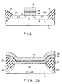
- Fig. 1 designates a conventional non-volatile memory presented for explaining the DSA structure.
- the reference numeral 11 designates a P-type silicon substrate, 12 oxidized film for separation, 13a a source region containing N+ type impurities, 13b a drain region containing N+ type impurities, 14 a floating gate, 15 a control gate, 16 a region containing P type impurities, 17 a channel region, 18 a gate insulation film, and 19 designates an insulation film between gate electrodes, respectively.
- the region 16 containing P type impurities having density stronger than that is present in the center of the channel region 17 is provided by way of surround the drain region 13b of an N-channel type cell transistor.
- the region 16 is hereinafter merely called the "P-pocket" region.
- profile of the density of impurities in the P-pocket region 16 adjacent to an edge of the drain region 13b of the floating gate is particularly important.
- the density of impurities in the P-pocket region 16 close to an edge of the drain region 13b must constantly be held stronger than that is present in the channel region 17. Nevertheless, since the P-pocket region 16 is formed by means of P-type impurities aides by injection of ion after completing the formation of stratified gate electrodes, it results in the occurrence of problem described below.
- the edge of the drain 13b is covered with stacked gate electrodes.
- a conventional ion injection method in order to prevent occurrence of "channeling effect", in other words, in order to prevent ion from deeply being injected beyond path which allows easy passage of ion, only a maximum of 7 degrees of angle is applied to the injection of ion against the normal of the silicon substrate 11, and thus, the P-type impurities cannot fully be injected into the region close to the drain region 13b below the floating gate 14.
- any conventional art injects ion needed for the formation of the P-pocket region 16, and then executes an annealing process to diffuse the P-type impurities into such region father than the edge of the drain region 13b below the channel region 17 before eventually injecting ion needed for the formation of the source and drain regions 13a and 13b.
- an additional round of annealing process is needed for the formation of the P-pocket region 16 containing the DSA structure.
- the junction breakdown voltage is determined by the breakdown voltage of a high P-type impurity region formed of the overlapping portions the P-pocket region and a channel stopper region located below an isolation region, and by the breakdown voltage of the pn junction formed between the N+ regions of the regions 13a and 13b. Because of this, the junction breakdown voltage is largely dependent on the distribution of the density of impurities present in those adjacent regions.
- the object of the invention is to provide a novel method of manufacturing a semiconductor device which promotes own capability of controlling profile of the density of P-type impurities in the drain or source regions adjoining the channel region of a stacked gate type non-volatile memory cell so that own performance capability can be promoted furthermore.
- the invention provides a novel method of manufacturing a semiconductor device comprising those sequential steps including the following; forming a floating gate electrode on an insulation film formed on a layer, said floating gate electrode located above that region of the layer in which a first conductivity type channel is to be formed, and forming a control gate on another insulation film formed on the floating gate electrode; and injecting ions of an impurity having a first conductivity type into a semiconductor substrate at an angle of at least 8° to the normal to the substrate, thereby to form a region having a high concentration of the first conductivity type impurity, in the vicinity of a boundary a diffusion layer which contains an impurity of a second conductivity type and which is to form a drain region of a transistor having said control gate electrode.
- the method embodied by the invention characteristically executes those sequential steps including the following;
- the system embodied by the invention continuously or intermittently rotates the semiconductor substrate while injecting impurities into superimposed gate electrode layers in conjunction with ion for the formation of a P-pocket region; next, the system injects ion into lateral surface of the superimposed gate electrode layers by applying a minimum of 8 degrees of angle in order to promote the density of impurities in the P-pocket region adjacent to the edge of the drain region below the floating gate electrode.
- the system embodied by the invention can securely vary voltage available for accelerating the ion injection speed and also vary the angle for injecting ion into the semiconductor substrate as well. Based on those techniques mentioned above, the system embodied by the invention simultaneously controls the profile of the density of impurities in the ion-injected region and the "short-channel" effect from occurrence, thus effectively promoting the data writing efficiency.
- the system embodied by the invention injects ion into the semiconductor substrate by applying a minimum of 8 degrees and a maximum of 60 degrees of angle against the normal of this substrate. This is because, like any conventional art, if ion were injected into the substrate at a maximum of 7 degrees of angle against the normal of the substrate, then the effect of strengthening the density of impurities will be minimized in the P-pocket region adjacent to the edge of the drain region below the floating gate electrode. Injection of ion at a minimum of 8 degrees of angle initiates promotion of density of impurities beyond the conventionally available level. Conversely, if the ion injection angle exceeds 60 degrees, then difficulty is present in the effect of fully injecting ion into the substrate. Since the system embodied by the invention injects ion at a minimum of 8 degrees against the normal of the substrate, the above-cited channel effect arises. Nevertheless, since ion is deeply injected, no critical problem arises.
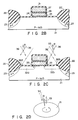
- the system embodied by the invention forms a field insulation film 22 and a channel stopper region 23 on the surface of a P-type silicone substrate 21, then separates elements.
- the P-type silicone substrate 21 is superficially provided with a gate insulation film 24 having about 20 nm of thickness.
- a gate insulation film 24 having about 20 nm of thickness.
- the art embodied by the invention forms the channel region merely by applying the P-type impurities held in the P-type silicone substrate 21 without injecting the ionized P-type impurities therein for strengthening the density.
- the system forms phosphor-doped polycrystalline silicon layer 25 on the gate insulation film 24, where this layer 24 is available for composing a floating gate electrode.
- thermally oxidized film 26 having about 20 nm of thickness is formed on the polycrystalline silicone layer 25 by applying a thermal oxidation process.
- the system forms the secondary phosphor-doped polycrystalline silicon layer 27 on the thermally oxidized film 26 (see Fig. 2A), where this layer 27 is available for composing a control gate electrode.
- the system injects the P-type impurities into the P-type silicon substrate 21 in conjunction with ion by way of self-aligned the stacked gate electrode unit serving as mask, and then forms up ion-injected P-type layers 32a and 32b adjoining those regions predetermined to become source and drain regions.
- Ion is injected into the P-type silicon substrate 21 while continuously rotating it more than 1 round per minute by injecting more than 5 ⁇ 1012 cm ⁇ 2 of a dosed amount of boron by applying 10 ⁇ ⁇ ⁇ 45 degrees of angle against the normal 33 of the silicone substrate 21 (see Fig. 2C and 2D).
- care be taken to inject ionized impurities by properly adjusting the density of impurities to be stronger than that is present in the center of the channel region and weaker than that is present in the drain region of this cell transistor.
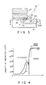
- the process of ion injection can be implemented in accordance with the method of manufacturing semiconductor device based on the condition specified by the expression shown below.
- X p designates the mean projected range of the P-type conductive impurities injected into the P-pocket region in conjunction with ion from the surface of the P-type silicone substrate;
- ⁇ designates the angle at which ion is injected against the normal of the P-type silicon substrate;
- X jl designates the extended distance of the edge of the drain or source region as a result of elongation in the direction of the channel region below the stacked gate electrode unit by effect of diffusion until reaching the final production step after completing the ion injection process (see Fig. 3).
- the density of impurities in the P-pocket region at the edge of the drain region can sufficiently be strengthened only when the product of tan ⁇ and the distance X p designating the mean projected range of the P-type impurities injected into the P-pocket region together with ion from the surface of the P-type silicone substrate is greater than the distance X jl designating the distance of the edge of the drain region diffused into the portion below the floating gate electrode. This allows the P-pocket region to fully exert own functional effect.
- the P-type impurities were not deeply injected, then it will cause the P-type impurities to be absorbed into the superficial oxidized film generated by the following thermal treatment including oxidation, thus resulting in the ineffective application of the P-type impurities.
- the P-pocket region is effective when the value of ⁇ is more than 28 degrees.
- the embodiment of the invention allows the P-type impurities to effectively be injected into the P-pocket region by applying a minimum of 8 degrees and a maximum of 60 degrees as well.
- the reference numeral 34 shown in Figs. 2C and 2D designates beam of ion containing P-type impurities.
- the reference numeral 36a and 36b designate ionized P-type impurities injected into field edge.
- the reference numeral 21 designates the rotating P-type silicon substrate.
- the P-type impurities contained in ion is injected into the substrate by way of self-aligned the stacked gate electrode unit functioning as mask, and then N-type ion-injected layers 39a and 39b are respectively formed.
- ion is injected into the P-type silicone substrate 21 so that the injection can be oriented in parallel with the lateral surface of the stacked gate electrode unit or at an angle of 7° to the normal to the surface of the silicon substrate 21.
- 5 ⁇ 1015 cm ⁇ 2 of a dosed amount of ionized arsenic is injected into the silicon substrate 21.
- the reference numeral 38 shown in Fig. 2E designates beam of ionized N-type impurities.
- a thermal process such as an annealing process is executed at 900°C in order to activate ionized impurities and recover the oxidized film 24, 31 from damage incurred from the said two injections of ion.
- the ion-injected P-type layers 32a and 32b respectively form P-pocket regions 40a and 40b.
- the ion-injected N-type layers 32a and 32b respectively form source and drain regions 41a and 41b.
- an insulation film 42 above the source and drain regions 41a and 41b is perforated to provide a contact hole 43.
- an aluminium electrode 44 is formed, thus completing the production of an EPROM cell (see Fig. 2F).
- the reference numeral 45 shown in Fig. 2F designates the portion where the P-pocket region and the channel stopper region overlap each other.
- the reference numeral 46 designates the channel region.
- the density of P-type impurities in the P-pocket region adjacent to the edge of the drain region can securely be strengthened, where the density of P-type impurities makes up the decisive factor of the DSA structure.
- the efficiency of writing data into the cell memory is promoted.
- "short-channel" effect is improved, thus easily allowing materialization of finer size of the cell and integration of densely built circuits as well.
- Fig. 3 designates the sectional views of those regions adjacent to the drain edge of the cell embodied by the invention.
- the P-pocket region shown in Fig. 3 with a broken line designates the case in which the conventional ion injection method is applied to the formation of the P-pocket region of the above embodiment.
- the reference character X j shown in Fig. 3 designates the depth of the junction of the drain region 41b, whereas X jl designates the extended distance of the edge of the drain or source region as a result of elongation in the direction of the channel region below the floating gate electrode by effect of diffusion until reaching the final production process after completing the ion injection process.
- Fig. 3 designates the sectional views of those regions adjacent to the drain edge of the cell embodied by the invention.
- the P-pocket region shown in Fig. 3 with a broken line designates the case in which the conventional ion injection method is applied to the formation of the P-pocket region of the above embodiment.
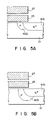
- FIG. 4 graphically designates concrete distribution of the density of impurities across the A-A' section shown in Fig. 3.
- the density of boron shown by means of a broken line designates the case in which the conventional ion injection method is applied to the formation of the P-pocket region of the above embodiment.
- the system of manufacturing the semiconductor device according to the invention provides those useful advantages described below.
- the scope of the invention is by no means confined to the embodiment thus far described, but the invention is also applicable to a variety of uses.
- the above embodiment has formed the P-pocket region by way of covering the source and drain regions (see Fig. 2F).
- the P-pocket region shown in Figs. 5A and 5B can also locally be provided via a masking process by causing the P-type silicon substrate 21 to stand sill or intermittently rotate itself.
- the description of the above embodiment has solely referred to the case of forming up the P-pocket region on both sides of the drain and source regions, it is quite apparent that the embodiment can also provide the P-pocket region solely on the part of the drain region or the source region via a masking process. Furthermore, although the above description has solely referred to the N-channel type cell transistor, the embodiment of the invention is also applicable to the P-channel type cell transistor as well.
Landscapes
- Non-Volatile Memory (AREA)
- Semiconductor Memories (AREA)
Applications Claiming Priority (2)
| Application Number | Priority Date | Filing Date | Title |
|---|---|---|---|
| JP6153190 | 1990-03-13 | ||
| JP61531/90 | 1990-03-13 |
Publications (2)
| Publication Number | Publication Date |
|---|---|
| EP0446893A1 true EP0446893A1 (de) | 1991-09-18 |
| EP0446893B1 EP0446893B1 (de) | 1997-05-21 |
Family
ID=13173783
Family Applications (1)
| Application Number | Title | Priority Date | Filing Date |
|---|---|---|---|
| EP91103833A Expired - Lifetime EP0446893B1 (de) | 1990-03-13 | 1991-03-13 | Verfahren zur Herstellung von Halbleiterbauelementen mit Floatinggates |
Country Status (4)
| Country | Link |
|---|---|
| US (1) | US5147811A (de) |
| EP (1) | EP0446893B1 (de) |
| KR (1) | KR940010930B1 (de) |
| DE (1) | DE69126156T2 (de) |
Cited By (10)
| Publication number | Priority date | Publication date | Assignee | Title |
|---|---|---|---|---|
| WO1995008843A1 (en) * | 1993-09-24 | 1995-03-30 | Vlsi Technology, Inc. | Latid implants for increasing the effective width of transistor elements in a semiconductor device |
| US5444279A (en) * | 1993-08-11 | 1995-08-22 | Micron Semiconductor, Inc. | Floating gate memory device having discontinuous gate oxide thickness over the channel region |
| EP0656663A3 (de) * | 1993-12-01 | 1995-08-30 | Nec Corp | Nichtflüssige-Halbleiterspeicheranordnung und Verfahren zur Löschung und Herstellung. |
| WO1995024057A3 (en) * | 1994-03-03 | 1995-11-23 | Rohm Corp | Low voltage one transistor flash eeprom cell using fowler-nordheim programming and erase |
| EP0696050A1 (de) * | 1994-07-18 | 1996-02-07 | STMicroelectronics S.r.l. | Nicht-flüchtiger EPROM und Flash-EEPROM-Speicher und Verfahren zu seiner Herstellung |
| GB2301709A (en) * | 1995-06-02 | 1996-12-11 | Hyundai Electronics Ind | Method of forming a junction in a flash eeprom cell |
| EP0731494A3 (de) * | 1995-03-08 | 1998-05-20 | Advanced Micro Devices, Inc. | Herstellungsverfahren für integrierten Schaltkreis unter Benutzung von Bor-Implantat |
| EP0744754A3 (de) * | 1995-05-25 | 1999-03-17 | AT&T Corp. | Verfahren und Vorrichtung für Injektion von heissen Ladungsträgern |
| US5895950A (en) * | 1993-09-06 | 1999-04-20 | U.S. Philips Corporation | Semiconductor device having a non-volatile memory and method of manufacturing such a semiconductor device |
| WO2000019511A1 (en) * | 1998-09-29 | 2000-04-06 | Advanced Micro Devices, Inc. | Deposition of oxide layer on the gate |
Families Citing this family (43)
| Publication number | Priority date | Publication date | Assignee | Title |
|---|---|---|---|---|
| US5258319A (en) * | 1988-02-19 | 1993-11-02 | Mitsubishi Denki Kabushiki Kaisha | Method of manufacturing a MOS type field effect transistor using an oblique ion implantation step |
| JPH05121763A (ja) * | 1991-10-30 | 1993-05-18 | Rohm Co Ltd | 半導体記憶装置の製造方法 |
| US5625212A (en) * | 1992-03-23 | 1997-04-29 | Matsushita Electric Industrial Co., Ltd. | Semiconductor memory device and method of manufacturing the same |
| US5432107A (en) * | 1992-11-04 | 1995-07-11 | Matsushita Electric Industrial Co., Ltd. | Semiconductor fabricating method forming channel stopper with diagonally implanted ions |
| JP3050717B2 (ja) * | 1993-03-24 | 2000-06-12 | シャープ株式会社 | 半導体装置の製造方法 |
| JPH06291181A (ja) * | 1993-03-30 | 1994-10-18 | Nippon Steel Corp | 半導体装置の製造方法 |
| JP2536413B2 (ja) * | 1993-06-28 | 1996-09-18 | 日本電気株式会社 | 半導体集積回路装置の製造方法 |
| US5372957A (en) * | 1993-07-22 | 1994-12-13 | Taiwan Semiconductor Manufacturing Company | Multiple tilted angle ion implantation MOSFET method |
| US5308780A (en) * | 1993-07-22 | 1994-05-03 | United Microelectronics Corporation | Surface counter-doped N-LDD for high hot carrier reliability |
| US5496747A (en) * | 1993-08-02 | 1996-03-05 | United Microelectronics Corporation | Split-gate process for non-volatile memory |
| US5432106A (en) * | 1993-08-02 | 1995-07-11 | United Microelectronics Corporation | Manufacture of an asymmetric non-volatile memory cell |
| EP0655778A3 (de) * | 1993-11-25 | 1996-01-03 | Matsushita Electronics Corp | Verfahren zur Herstellung von Halbleiterspeicheranordnungen. |
| US5409848A (en) * | 1994-03-31 | 1995-04-25 | Vlsi Technology, Inc. | Angled lateral pocket implants on p-type semiconductor devices |
| US5441906A (en) * | 1994-04-04 | 1995-08-15 | Motorola, Inc. | Insulated gate field effect transistor having a partial channel and method for fabricating |
| US5427964A (en) * | 1994-04-04 | 1995-06-27 | Motorola, Inc. | Insulated gate field effect transistor and method for fabricating |
| US5482878A (en) * | 1994-04-04 | 1996-01-09 | Motorola, Inc. | Method for fabricating insulated gate field effect transistor having subthreshold swing |
| US5543337A (en) * | 1994-06-15 | 1996-08-06 | Lsi Logic Corporation | Method for fabricating field effect transistor structure using symmetrical high tilt angle punchthrough implants |
| US5413945A (en) * | 1994-08-12 | 1995-05-09 | United Micro Electronics Corporation | Blanket N-LDD implantation for sub-micron MOS device manufacturing |
| US5468981A (en) * | 1994-09-01 | 1995-11-21 | Advanced Micro Devices, Inc. | Self-aligned buried channel/junction stacked gate flash memory cell |
| US5700728A (en) * | 1994-11-07 | 1997-12-23 | United Microelectronics Corporation | Method of forming an MNOS/MONOS by employing large tilt angle ion implantation underneath the field oxide |
| US5801076A (en) * | 1995-02-21 | 1998-09-01 | Advanced Micro Devices, Inc. | Method of making non-volatile memory device having a floating gate with enhanced charge retention |
| KR970004074A (ko) * | 1995-06-05 | 1997-01-29 | 빈센트 비. 인그라시아 | 절연 게이트 전계 효과 트랜지스터 및 그 제조 방법 |
| JPH09148542A (ja) * | 1995-11-17 | 1997-06-06 | Sharp Corp | 半導体記憶装置及びその製造方法 |
| US5719425A (en) * | 1996-01-31 | 1998-02-17 | Micron Technology, Inc. | Multiple implant lightly doped drain (MILDD) field effect transistor |
| US5849615A (en) | 1996-02-22 | 1998-12-15 | Micron Technology, Inc. | Semiconductor processing method of fabricating field effect transistors |
| US6346439B1 (en) | 1996-07-09 | 2002-02-12 | Micron Technology, Inc. | Semiconductor transistor devices and methods for forming semiconductor transistor devices |
| US5793088A (en) * | 1996-06-18 | 1998-08-11 | Integrated Device Technology, Inc. | Structure for controlling threshold voltage of MOSFET |
| US5770880A (en) * | 1996-09-03 | 1998-06-23 | Harris Corporation | P-collector H.V. PMOS switch VT adjusted source/drain |
| US6236085B1 (en) | 1996-11-11 | 2001-05-22 | Denso Corporation | Semiconductor memory device having high-concentration region around electric-field moderating layer in substrate |
| US5998274A (en) * | 1997-04-10 | 1999-12-07 | Micron Technology, Inc. | Method of forming a multiple implant lightly doped drain (MILDD) field effect transistor |
| US6127222A (en) * | 1997-12-16 | 2000-10-03 | Advanced Micro Devices, Inc. | Non-self-aligned side channel implants for flash memory cells |
| US6103602A (en) * | 1997-12-17 | 2000-08-15 | Advanced Micro Devices, Inc. | Method and system for providing a drain side pocket implant |
| US6087219A (en) * | 1998-06-19 | 2000-07-11 | Taiwan Semiconductor Manufacturing Company | Highly reliable flash memory structure with halo source |
| JP3264323B2 (ja) * | 1998-07-31 | 2002-03-11 | 日本電気株式会社 | リバースプロファイリング方法 |
| US6284603B1 (en) * | 2000-07-12 | 2001-09-04 | Chartered Semiconductor Manufacturing Inc. | Flash memory cell structure with improved channel punch-through characteristics |
| US6524914B1 (en) * | 2000-10-30 | 2003-02-25 | Advanced Micro Devices, Inc. | Source side boron implanting and diffusing device architecture for deep sub 0.18 micron flash memory |
| KR100373855B1 (ko) | 2001-01-20 | 2003-02-26 | 삼성전자주식회사 | 낸드형 플래시 메모리 장치 및 그 형성방법 |
| US6673664B2 (en) * | 2001-10-16 | 2004-01-06 | Sharp Laboratories Of America, Inc. | Method of making a self-aligned ferroelectric memory transistor |
| US6878589B1 (en) * | 2003-05-06 | 2005-04-12 | Advanced Micro Devices, Inc. | Method and system for improving short channel effect on a floating gate device |
| US7393752B2 (en) * | 2005-07-25 | 2008-07-01 | Freescale Semiconductor, Inc. | Semiconductor devices and method of fabrication |
| EP2400547B1 (de) * | 2009-02-18 | 2016-11-23 | Nanjing University | Lichtempfindlicher detektor mit mosfet mit dielektrischem verbundgate und signalleseverfahren dafür |
| KR101974439B1 (ko) | 2012-06-11 | 2019-05-02 | 삼성전자 주식회사 | 반도체 장치 및 그 제조 방법 |
| CN107710417B (zh) | 2015-06-16 | 2021-06-11 | 三菱电机株式会社 | 半导体装置的制造方法 |
Citations (3)
| Publication number | Priority date | Publication date | Assignee | Title |
|---|---|---|---|---|
| US4232439A (en) * | 1976-11-30 | 1980-11-11 | Vlsi Technology Research Association | Masking technique usable in manufacturing semiconductor devices |
| US4771012A (en) * | 1986-06-13 | 1988-09-13 | Matsushita Electric Industrial Co., Ltd. | Method of making symmetrically controlled implanted regions using rotational angle of the substrate |
| EP0333583A2 (de) * | 1988-03-14 | 1989-09-20 | Fujitsu Limited | Verfahren zur Herstellung einer Halbleitervorrichtung |
Family Cites Families (3)
| Publication number | Priority date | Publication date | Assignee | Title |
|---|---|---|---|---|
| JPS57130475A (en) * | 1981-02-06 | 1982-08-12 | Mitsubishi Electric Corp | Semiconductor memory storage and its manufacture |
| JPS5893279A (ja) * | 1981-11-30 | 1983-06-02 | Fujitsu Ltd | 半導体装置の製造方法 |
| JPS5961185A (ja) * | 1982-09-30 | 1984-04-07 | Fujitsu Ltd | Mis電界効果半導体装置の製造方法 |
-
1991
- 1991-03-07 KR KR1019910003652A patent/KR940010930B1/ko not_active Expired - Fee Related
- 1991-03-11 US US07/666,912 patent/US5147811A/en not_active Expired - Lifetime
- 1991-03-13 DE DE69126156T patent/DE69126156T2/de not_active Expired - Fee Related
- 1991-03-13 EP EP91103833A patent/EP0446893B1/de not_active Expired - Lifetime
Patent Citations (3)
| Publication number | Priority date | Publication date | Assignee | Title |
|---|---|---|---|---|
| US4232439A (en) * | 1976-11-30 | 1980-11-11 | Vlsi Technology Research Association | Masking technique usable in manufacturing semiconductor devices |
| US4771012A (en) * | 1986-06-13 | 1988-09-13 | Matsushita Electric Industrial Co., Ltd. | Method of making symmetrically controlled implanted regions using rotational angle of the substrate |
| EP0333583A2 (de) * | 1988-03-14 | 1989-09-20 | Fujitsu Limited | Verfahren zur Herstellung einer Halbleitervorrichtung |
Non-Patent Citations (2)
| Title |
|---|
| JOURNAL OF ELECTRONIC ENGINEERING vol. 26, no. 267, March 1989, pages 128-131, Tokyo, JP; T. HORI et al.: "A New Submicron p-Channel MOSFET with LATIPS (Large-Tilt-Angle Implanted Punchthrough Stopper)" * |
| PATENT ABSTRACTS OF JAPAN vol. 6, no. 230 (E-142)(1108), 16 November 1982; & JP - A - 57130475 (MITSUBISHI DENKI) 12.08.1982 * |
Cited By (19)
| Publication number | Priority date | Publication date | Assignee | Title |
|---|---|---|---|---|
| US5444279A (en) * | 1993-08-11 | 1995-08-22 | Micron Semiconductor, Inc. | Floating gate memory device having discontinuous gate oxide thickness over the channel region |
| US5604366A (en) * | 1993-08-11 | 1997-02-18 | Micron Technology, Inc. | Floating gate memory device having discontinuous gate oxide thickness over the channel region |
| US5895950A (en) * | 1993-09-06 | 1999-04-20 | U.S. Philips Corporation | Semiconductor device having a non-volatile memory and method of manufacturing such a semiconductor device |
| WO1995008843A1 (en) * | 1993-09-24 | 1995-03-30 | Vlsi Technology, Inc. | Latid implants for increasing the effective width of transistor elements in a semiconductor device |
| EP0656663A3 (de) * | 1993-12-01 | 1995-08-30 | Nec Corp | Nichtflüssige-Halbleiterspeicheranordnung und Verfahren zur Löschung und Herstellung. |
| US5535158A (en) * | 1993-12-01 | 1996-07-09 | Nec Corporation | Non-volatile semiconductor memory device and method for erasure and production thereof |
| WO1995024057A3 (en) * | 1994-03-03 | 1995-11-23 | Rohm Corp | Low voltage one transistor flash eeprom cell using fowler-nordheim programming and erase |
| EP0933821A3 (de) * | 1994-03-03 | 1999-08-11 | Rohm Corporation | Niederspannungs-Eintransistor-FLASH-EEPROM-Zelle mit Fowler-Nordheim Programmier- und Löschung |
| US5587947A (en) * | 1994-03-03 | 1996-12-24 | Rohm Corporation | Low voltage one transistor flash EEPROM cell using Fowler-Nordheim programming and erase |
| US5687120A (en) * | 1994-03-03 | 1997-11-11 | Rohn Corporation | Low voltage one transistor flash eeprom cell using fowler-nordheim programming and erase |
| US5689459A (en) * | 1994-03-03 | 1997-11-18 | Rohm Corporation | Low voltage one transistor flash EEPROM cell using Fowler-Nordheim programming and erase |
| EP0696050A1 (de) * | 1994-07-18 | 1996-02-07 | STMicroelectronics S.r.l. | Nicht-flüchtiger EPROM und Flash-EEPROM-Speicher und Verfahren zu seiner Herstellung |
| US5712814A (en) * | 1994-07-18 | 1998-01-27 | Sgs-Thomson Microelectronics S.R.L. | Nonvolatile memory cell and a method for forming the same |
| US5920776A (en) * | 1994-07-18 | 1999-07-06 | Sgs-Thomson Microelectronics, S.R.L. | Method of making asymmetric nonvolatile memory cell |
| EP0731494A3 (de) * | 1995-03-08 | 1998-05-20 | Advanced Micro Devices, Inc. | Herstellungsverfahren für integrierten Schaltkreis unter Benutzung von Bor-Implantat |
| EP0744754A3 (de) * | 1995-05-25 | 1999-03-17 | AT&T Corp. | Verfahren und Vorrichtung für Injektion von heissen Ladungsträgern |
| GB2301709B (en) * | 1995-06-02 | 1999-04-21 | Hyundai Electronics Ind | Method of forming a junction in a flash eeprom cell |
| GB2301709A (en) * | 1995-06-02 | 1996-12-11 | Hyundai Electronics Ind | Method of forming a junction in a flash eeprom cell |
| WO2000019511A1 (en) * | 1998-09-29 | 2000-04-06 | Advanced Micro Devices, Inc. | Deposition of oxide layer on the gate |
Also Published As
| Publication number | Publication date |
|---|---|
| KR940010930B1 (ko) | 1994-11-19 |
| DE69126156T2 (de) | 1997-10-09 |
| DE69126156D1 (de) | 1997-06-26 |
| EP0446893B1 (de) | 1997-05-21 |
| US5147811A (en) | 1992-09-15 |
Similar Documents
| Publication | Publication Date | Title |
|---|---|---|
| US5147811A (en) | Method of manufacturing semiconductor device by controlling the profile of the density of p-type impurities in the source/drain regions | |
| US4342149A (en) | Method of making very short channel length MNOS and MOS devices by double implantation of one conductivity type subsequent to other type implantation | |
| KR930008007B1 (ko) | Rom 제조방법 | |
| EP0164449B1 (de) | Verfahren zum Herstellen einer integrierten Halbleiterschaltkreisanordnung mit einem MISFET | |
| US5337274A (en) | Nonvolatile semiconductor memory device having adjacent memory cells and peripheral transistors separated by field oxide | |
| US5925914A (en) | Asymmetric S/D structure to improve transistor performance by reducing Miller capacitance | |
| KR0137625B1 (ko) | 매립 채널형 mos 트랜지스터 및 그 제조방법 | |
| KR20000069811A (ko) | 임계전압을 승압하는 웰 부스팅 | |
| JP2558961B2 (ja) | 半導体装置の製造方法 | |
| US4330850A (en) | MNOS Memory cell | |
| US5397727A (en) | Method of forming a floating gate programmable read only memory cell transistor | |
| EP0459398B1 (de) | Herstellungsverfahren eines Kanals in MOS-Halbleiteranordnung | |
| EP0452817B1 (de) | Halbleiterbauelement mit MOS-Transistoren und Verfahren zu dessen Herstellung | |
| KR100194008B1 (ko) | 다양한 종류의 mosfet를 갖는 반도체 장치 제조방법 | |
| JPH0210775A (ja) | イオン注入半導体デバイス | |
| JP2562688B2 (ja) | 半導体装置の製造方法 | |
| US6509237B2 (en) | Flash memory cell fabrication sequence | |
| JP2727590B2 (ja) | Mis型半導体装置 | |
| JP2595058B2 (ja) | 不揮発性半導体記憶装置の製造方法 | |
| KR100233294B1 (ko) | 반도체 메모리소자 및 그 제조방법 | |
| KR100624922B1 (ko) | 플래쉬 메모리 소자의 제조방법 | |
| KR100217899B1 (ko) | 반도체 소자의 트랜지스터 제조 방법 | |
| JP2957586B2 (ja) | 不揮発性メモリセルの製造方法 | |
| JP2880885B2 (ja) | 半導体集積回路装置及びその製造方法 | |
| KR100204800B1 (ko) | 모스 트랜지스터 제조방법 |
Legal Events
| Date | Code | Title | Description |
|---|---|---|---|
| PUAI | Public reference made under article 153(3) epc to a published international application that has entered the european phase |
Free format text: ORIGINAL CODE: 0009012 |
|
| 17P | Request for examination filed |
Effective date: 19910313 |
|
| AK | Designated contracting states |
Kind code of ref document: A1 Designated state(s): DE FR GB |
|
| 17Q | First examination report despatched |
Effective date: 19950126 |
|
| GRAG | Despatch of communication of intention to grant |
Free format text: ORIGINAL CODE: EPIDOS AGRA |
|
| GRAH | Despatch of communication of intention to grant a patent |
Free format text: ORIGINAL CODE: EPIDOS IGRA |
|
| GRAH | Despatch of communication of intention to grant a patent |
Free format text: ORIGINAL CODE: EPIDOS IGRA |
|
| GRAA | (expected) grant |
Free format text: ORIGINAL CODE: 0009210 |
|
| AK | Designated contracting states |
Kind code of ref document: B1 Designated state(s): DE FR GB |
|
| REF | Corresponds to: |
Ref document number: 69126156 Country of ref document: DE Date of ref document: 19970626 |
|
| ET | Fr: translation filed | ||
| PGFP | Annual fee paid to national office [announced via postgrant information from national office to epo] |
Ref country code: FR Payment date: 19980310 Year of fee payment: 8 |
|
| PLBE | No opposition filed within time limit |
Free format text: ORIGINAL CODE: 0009261 |
|
| STAA | Information on the status of an ep patent application or granted ep patent |
Free format text: STATUS: NO OPPOSITION FILED WITHIN TIME LIMIT |
|
| 26N | No opposition filed | ||
| REG | Reference to a national code |
Ref country code: GB Ref legal event code: 746 Effective date: 19981008 |
|
| PG25 | Lapsed in a contracting state [announced via postgrant information from national office to epo] |
Ref country code: DE Free format text: LAPSE BECAUSE OF NON-PAYMENT OF DUE FEES Effective date: 19981201 |
|
| PG25 | Lapsed in a contracting state [announced via postgrant information from national office to epo] |
Ref country code: FR Free format text: LAPSE BECAUSE OF NON-PAYMENT OF DUE FEES Effective date: 19991130 |
|
| REG | Reference to a national code |
Ref country code: FR Ref legal event code: ST |
|
| REG | Reference to a national code |
Ref country code: GB Ref legal event code: IF02 |
|
| PGFP | Annual fee paid to national office [announced via postgrant information from national office to epo] |
Ref country code: GB Payment date: 20070307 Year of fee payment: 17 |
|
| GBPC | Gb: european patent ceased through non-payment of renewal fee |
Effective date: 20080313 |
|
| PG25 | Lapsed in a contracting state [announced via postgrant information from national office to epo] |
Ref country code: GB Free format text: LAPSE BECAUSE OF NON-PAYMENT OF DUE FEES Effective date: 20080313 |