EP0448471A2 - Verfahren zur Planarisierung einer Metallschicht - Google Patents
Verfahren zur Planarisierung einer Metallschicht Download PDFInfo
- Publication number
- EP0448471A2 EP0448471A2 EP91400759A EP91400759A EP0448471A2 EP 0448471 A2 EP0448471 A2 EP 0448471A2 EP 91400759 A EP91400759 A EP 91400759A EP 91400759 A EP91400759 A EP 91400759A EP 0448471 A2 EP0448471 A2 EP 0448471A2
- Authority
- EP
- European Patent Office
- Prior art keywords
- layer
- alignment mark
- semiconductor
- metal
- planarization method
- Prior art date
- Legal status (The legal status is an assumption and is not a legal conclusion. Google has not performed a legal analysis and makes no representation as to the accuracy of the status listed.)
- Granted
Links
Images



Classifications
-
- H—ELECTRICITY
- H10—SEMICONDUCTOR DEVICES; ELECTRIC SOLID-STATE DEVICES NOT OTHERWISE PROVIDED FOR
- H10P—GENERIC PROCESSES OR APPARATUS FOR THE MANUFACTURE OR TREATMENT OF DEVICES COVERED BY CLASS H10
- H10P95/00—Generic processes or apparatus for manufacture or treatments not covered by the other groups of this subclass
- H10P95/04—Planarisation of conductive or resistive materials
-
- H—ELECTRICITY
- H10—SEMICONDUCTOR DEVICES; ELECTRIC SOLID-STATE DEVICES NOT OTHERWISE PROVIDED FOR
- H10P—GENERIC PROCESSES OR APPARATUS FOR THE MANUFACTURE OR TREATMENT OF DEVICES COVERED BY CLASS H10
- H10P34/00—Irradiation with electromagnetic or particle radiation of wafers, substrates or parts of devices
- H10P34/40—Irradiation with electromagnetic or particle radiation of wafers, substrates or parts of devices with high-energy radiation
- H10P34/42—Irradiation with electromagnetic or particle radiation of wafers, substrates or parts of devices with high-energy radiation with electromagnetic radiation, e.g. laser annealing
-
- H—ELECTRICITY
- H10—SEMICONDUCTOR DEVICES; ELECTRIC SOLID-STATE DEVICES NOT OTHERWISE PROVIDED FOR
- H10W—GENERIC PACKAGES, INTERCONNECTIONS, CONNECTORS OR OTHER CONSTRUCTIONAL DETAILS OF DEVICES COVERED BY CLASS H10
- H10W20/00—Interconnections in chips, wafers or substrates
- H10W20/01—Manufacture or treatment
- H10W20/031—Manufacture or treatment of conductive parts of the interconnections
- H10W20/062—Manufacture or treatment of conductive parts of the interconnections by smoothing of conductive parts, e.g. by planarisation
-
- H—ELECTRICITY
- H10—SEMICONDUCTOR DEVICES; ELECTRIC SOLID-STATE DEVICES NOT OTHERWISE PROVIDED FOR
- H10W—GENERIC PACKAGES, INTERCONNECTIONS, CONNECTORS OR OTHER CONSTRUCTIONAL DETAILS OF DEVICES COVERED BY CLASS H10
- H10W46/00—Marks applied to devices, e.g. for alignment or identification
-
- H—ELECTRICITY
- H10—SEMICONDUCTOR DEVICES; ELECTRIC SOLID-STATE DEVICES NOT OTHERWISE PROVIDED FOR
- H10W—GENERIC PACKAGES, INTERCONNECTIONS, CONNECTORS OR OTHER CONSTRUCTIONAL DETAILS OF DEVICES COVERED BY CLASS H10
- H10W46/00—Marks applied to devices, e.g. for alignment or identification
- H10W46/301—Marks applied to devices, e.g. for alignment or identification for alignment
-
- H—ELECTRICITY
- H10—SEMICONDUCTOR DEVICES; ELECTRIC SOLID-STATE DEVICES NOT OTHERWISE PROVIDED FOR
- H10W—GENERIC PACKAGES, INTERCONNECTIONS, CONNECTORS OR OTHER CONSTRUCTIONAL DETAILS OF DEVICES COVERED BY CLASS H10
- H10W46/00—Marks applied to devices, e.g. for alignment or identification
- H10W46/501—Marks applied to devices, e.g. for alignment or identification for use before dicing
-
- Y—GENERAL TAGGING OF NEW TECHNOLOGICAL DEVELOPMENTS; GENERAL TAGGING OF CROSS-SECTIONAL TECHNOLOGIES SPANNING OVER SEVERAL SECTIONS OF THE IPC; TECHNICAL SUBJECTS COVERED BY FORMER USPC CROSS-REFERENCE ART COLLECTIONS [XRACs] AND DIGESTS
- Y10—TECHNICAL SUBJECTS COVERED BY FORMER USPC
- Y10S—TECHNICAL SUBJECTS COVERED BY FORMER USPC CROSS-REFERENCE ART COLLECTIONS [XRACs] AND DIGESTS
- Y10S148/00—Metal treatment
- Y10S148/093—Laser beam treatment in general
-
- Y—GENERAL TAGGING OF NEW TECHNOLOGICAL DEVELOPMENTS; GENERAL TAGGING OF CROSS-SECTIONAL TECHNOLOGIES SPANNING OVER SEVERAL SECTIONS OF THE IPC; TECHNICAL SUBJECTS COVERED BY FORMER USPC CROSS-REFERENCE ART COLLECTIONS [XRACs] AND DIGESTS
- Y10—TECHNICAL SUBJECTS COVERED BY FORMER USPC
- Y10S—TECHNICAL SUBJECTS COVERED BY FORMER USPC CROSS-REFERENCE ART COLLECTIONS [XRACs] AND DIGESTS
- Y10S438/00—Semiconductor device manufacturing: process
- Y10S438/975—Substrate or mask aligning feature
Definitions
- the present invention generally relates to planarization methods, and more particularly to a method of planarizing a metal layer by a pulse energy beam such as a pulse laser beam.
- the method of the present invention is especially suited for planarizing a metal interconnection layer.
- a conductor layer 4 shown in FIG.1 is formed on an insulator layer 2 which is provided on a semiconductor layer 1 by a vapor deposition, sputtering or the like.
- a via hole 5 such as a contact hole and a through hole in the insulator layer 2 becomes smaller, the conductor layer 4 does not sufficiently fill the via hole 5 and the step coverage becomes poor. This poor step coverage is caused by the fact that it becomes difficult for the conductor layer 4 to adhere on the sidewall of the via hole 5 due to the shadowing effect.
- FIG.2 is a cross sectional view for explaining a proposed method of eliminating the poor step coverage described above. According to this proposed method, a laser beam is irradiated on the conductor layer 4 to melt and planarize the conductor layer 4.
- FIGS.3 and 4 are cross sectional views for explaining a proposed method of forming a plug to eliminate the problem of poor step coverage.
- the conductor layer 4 is formed in a vicinity of the via hole 5 as shown in FIG.3, and a laser beam is irradiated on the conductor layer 4 to form a plug 6 within the via hole 5 by the melted conductor as shown in FIG.4.
- an alignment mark 3 is usually formed on the conductor layer 4 as shown in FIG.5.
- This alignment mark 3 is used for aligning a mask relative to the conductor layer 4.
- the laser beam irradiates the conductor layer 4
- the laser beam irradiates the entire surface of the conductor layer 4 because the laser beam irradiation is made with respect to the conductor layer 4 on a wafer, for example, so as to improve the throughput of the device.
- the alignment mark 3 is also planarized by the laser beam irradiation as shown in FIG.6, and there is a problem in that the alignment mark 3 disappears when the planarization using the laser beam is carried out.
- the laser beam irradiation is made to avoid the alignment mark 3, it is necessary to irradiate the laser beam on the conductor layer 4 on the wafer in parts, and the throughput of the device becomes poor because of the need to make several laser beam irradiations with respect to the conductor layer 4 on the wafer.
- Another and more specific object of the present invention is to provide a planarization method comprising the steps of forming a second layer on a first layer which has an alignment mark having a heat sink structure, where the second layer is made of a metal, and irradiating a pulse energy beam on the entire exposed surface of the second layer to planarize the second layer, where heat generated in the second layer on the alignment mark is released via the first layer so that substantially no melting of the second layer occurs on the alignment mark.
- the planarization method of the present invention it is possible to prevent the alignment mark from being planarized by the energy beam irradiation.
- no alignment is required when carrying out the energy beam irradiation for the purpose of preventing the planarization of the alignment mark, and as a result, the throughput of the device is improved and the production cost is reduced.
- Still another object of the present invention is to provide a planarization method comprising the steps of patterning one or a plurality of second layers which are formed on a first layer having an alignment mark so as to remove the one or the plurality of second layers on the alignment mark thereby exposing the alignment mark provided on the first layer, where the alignment mark has a heat sink structure, forming a third layer on a top one of the second layers and the exposed surface of the first layer, where the third layer is made of a metal, and irradiating a pulse energy beam on the entire exposed surface of the third layer to planarize the third layer, where heat generated in the third layer on the alignment mark is released via the first layer so that substantially no melting of the third layer occurs on the alignment mark.
- a further object of the present invention is to provide a planarization method comprising the steps of patterning a second layer which is formed on a first layer so as to form an alignment mark having a heat sink structure thereby exposing a surface of the first layer, where the second layer is made of an insulator, forming a third layer on the second layer and the exposed surface of the first layer, and irradiating a pulse energy beam on the entire exposed surface of the third layer to planarize the third layer, where heat generated in the third layer on the alignment mark is released via the first layer so that substantially no melting of the third layer occurs on the alignment mark.
- Another object of the present invention is to provide a planarization method comprising the steps of forming a second layer on a first layer which has an alignment mark, where the second layer is made of a metal, removing the second layer in a vicinity of the alignment mark, and irradiating a pulse energy beam on the entire exposed surface of the second layer to planarize the second layer.
- Still another object of the present invention is to provide a planarization method comprising the steps of patterning one or a plurality of second layers which are formed on a first layer having an alignment mark so as to remove the one or the plurality of second layers on the alignment mark thereby exposing the alignment mark provided on the first layer, forming a third layer on a top one of the second layers and the exposed surface of the first layer, where the third layer is made of a metal, removing the third layer in a vicinity of the alignment mark, and irradiating a pulse energy beam on the entire exposed surface of the third layer to planarize the third layer.
- a further object of the present invention is to provide a planarization method comprising the steps of patterning a second layer which is formed on a first layer so as to form at least an alignment mark thereby exposing a surface of the first layer, where the second layer being made of an insulator, forming a third layer on at least the second layer, removing the third layer in a vicinity of the alignment mark provided on the second layer, and irradiating a pulse energy beam on the entire exposed surface of the third layer to planarize the third layer.
- Another object of the present invention is to provide a method of producing a semiconductor device comprising the steps of patterning one or a plurality of insulator layers which are formed on a semiconductor layer having an alignment mark and a semiconductor device so as to remove the one or the plurality of insulator layers on the alignment mark thereby exposing the alignment mark provided on the semiconductor layer, where said alignment mark has a heat sink structure, forming a metal layer on a top one of the insulator layers and the exposed surface of the semiconductor layer, and irradiating a pulse energy beam on the entire exposed surface of the metal layer to planarize the metal layer, where heat generated in the metal layer on the alignment mark is released via the semiconductor layer so that substantially no melting of the metal layer occurs on the alignment mark.
- Still another object of the present invention is to provide a method of producing a semiconductor device comprising the steps of patterning an insulator layer which is formed on a semiconductor layer having a semiconductor device so as to form an alignment mark having a heat sink structure thereby exposing a surface of the semiconductor layer, forming a metal layer on the insulator layer and the exposed surface of the semiconductor layer, and irradiating a pulse energy beam on the entire exposed surface of the metal layer to planarize the metal layer, where heat generated in the metal layer on the alignment mark is released via the semiconductor layer so that substantially no melting of the metal layer occurs on the alignment mark.
- a further object of the present invention is to provide a method of producing a semiconductor device comprising the steps of patterning one or a plurality of insulator layers which are formed on a semiconductor layer having an alignment mark and a semiconductor device so as to remove the one or the plurality of semiconductor layers on the alignment mark thereby exposing the alignment mark provided on the semiconductor layer, forming a metal layer on a top one of the insulator layers and the exposed surface of the semiconductor layer, removing the metal layer in a vicinity of the alignment mark, and irradiating a pulse energy beam on the entire exposed surface of the metal layer to planarize the metal layer.
- Another object of the present invention is to provide a method of producing a semiconductor device comprising the steps of patterning an insulator layer which is formed on a semiconductor layer having a semiconductor element so as to form at least an alignment mark thereby exposing a surface of the semiconductor layer, forming a metal layer on at least the insulator layer, removing the metal layer in a vicinity of the alignment mark which is provided on the insulator layer, and irradiating a pulse energy beam on the entire exposed surface of the metal layer to planarize the metal layer.
- an insulator layer 2 is formed on a semiconductor substrate 1.
- the insulator layer 2 is made of phospho-silicate glass (PSG) and has a thickness of 0.6 ⁇ m in this embodiment.
- the insulator layer 2 is patterned to form an alignment mark 3A and a via hole (not shown).
- the alignment mark 3A has a heat sink structure such that an area in which the insulator layer 2 is removed is sufficiently large.
- a conductor layer 4 is formed on the entire surface of the insulator layer 2 and the exposed surface of the semiconductor substrate 1.
- the conductor layer 4 is made of aluminum (Al) and has a thickness of 1.0 ⁇ m in this embodiment.
- a XeCl excimer laser beam is irradiated on the conductor layer 4 with a pulse energy of 7 J/cm2 to melt the Al.
- the melted Al completely fills the via hole and is planarized.
- the Al conductor layer 4 on the alignment mark 3A does not melt because the heat generated by the laser beam irradiation is released via the semiconductor substrate 1.
- the heat generated in the Al conductor layer 4 at the alignment mark 3A that is, at the heat sink structure, is effectively released via the semiconductor substrate 1.
- the alignment mark 3A will not be planarized by the laser beam irradiation.
- the planarized conductor layer 4 is then patterned using the alignment mark 3A so as to form an interconnection layer, for example.
- FIG.8 a description will be given of a second embodiment of the planarization method according to the present invention, by referring to FIG.8.
- FIG.8 and FIGS.9 through 11 which follow, those parts which are basically the same as those corresponding parts in FIG.7 are designated by the same reference numerals, and a description thereof will be omitted.
- a groove pattern is formed in the semiconductor substrate 1 so as to form an alignment mark 3B having a heat sink structure.
- the groove pattern has a depth of 0.5 ⁇ m.
- One or a plurality of layers may be formed on the semiconductor substrate 1 prior to forming the conductor layer 4. In such cases, each layer above the alignment mark 3B is removed when the layer is patterned before the conductor layer 4 is formed.
- the conductor layer 4 is made of Al and has a thickness of 1.0 ⁇ m. A laser beam is irradiated on the conductor layer 4 similarly to the first embodiment, so as to planarize the conductor layer 4.
- the heat generated in the Al conductor layer 4 on the alignment mark 3B is released via the semiconductor substrate 1, and the Al conductor layer 4 in this region does not melt. Accordingly, the alignment mark 3B will not be planarized by the laser beam irradiation.
- the planarized conductor layer 4 is then patterned using the alignment mark 3B so as to form an interconnection layer, for example.
- the insulator layer 2 formed on the semiconductor substrate 1 is made of PSG and has a thickness of 0.6 ⁇ m.
- the insulator layer 2 is patterned to form an alignment mark 3C and a via hole (not shown).
- the conductor layer 4 is formed on the entire surface of the insulator layer 2 and the exposed surface of the semiconductor substrate 1.
- the conductor layer 4 is made of Al. Thereafter, the conductor layer 4 is patterned to remove the conductor layer 4 on the alignment mark 3C.
- a laser beam is irradiated on the conductor layer 4 to melt the Al, similarly as in the case of the first embodiment.
- the melted Al completely fills the via hole and is planarized.
- the Al conductor layer 4 does not exist on the alignment mark 3C, and as a result, the alignment mark 3C will not be planarized by the laser beam irradiation.
- the planarized conductor layer 4 is then patterned using the alignment mark 3C so as to form an interconnection layer, for example.
- the insulator layer 2 formed on the semiconductor substrate 1 is made of PSG and has a thickness of 0.6 ⁇ m.
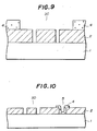
- the insulator layer 2 is patterned to form an alignment mark 3D and a via hole 5.
- the conductor layer 4 is formed on the entire surface of the insulator layer 2 and the exposed surface of the semiconductor substrate 1.
- the conductor layer 4 is made of Al. Thereafter, the conductor layer 4 is patterned so that the conductor layer 4 remains only in a vicinity of the via hole 5 as shown in FIG.10.
- a laser beam is irradiated on the conductor layer 4 to melt the Al, similarly as in the case of the first embodiment.
- the melted Al (conductor layer 4) in the vicinity of the via hole 5 flows into the via hole 5 and solidifies into a plug 6 as shown in FIG.11. Since the conductor layer 4 does not exist on the alignment mark 3D, the alignment mark 3D will not be planarized.
- an Al layer (not shown) which connects to the plug 6 is formed and patterned to form an interconnection layer, for example.
- the conductor layer 4 simply needs to be patterned to remove the conductor layer 4 in the vicinity of the alignment marks 3C and 3D. Since the patterning of the conductor layer 4 is originally required to leave the conductor layer 4 at least in the vicinity of the via hole 5, the process of removing the conductor layer 4 in the vicinity of the alignment marks 3C and 3D may be carried out simultaneously as the patterning to avoid the unnecessary increase of production processes.
- the conductor layer 4 in the vicinity of the alignment mark 3B shown in FIG.8 may be removed prior to the laser beam irradiation, to obtain substantially the same effects as the third embodiment.
- the conductor layer is made of Al.
- the conductor layer is not limited to Al, and any metal may be used.
- titanium (Ti), copper (Cu), tungsten (W) and molybdenum (Mo) may be used for the conductor layer.
- the melting of the conductor may of course be made by an energy beam other than the laser beam.
- the energy beam is a pulse energy beam.
- the semiconductor layer or substrate used in the described embodiments may be used as an active layer in which various semiconductor devices are formed.
- the illustration of such semiconductor devices will be omitted in this specification so as to simplify the drawings.
Landscapes
- Internal Circuitry In Semiconductor Integrated Circuit Devices (AREA)
- Exposure And Positioning Against Photoresist Photosensitive Materials (AREA)
Applications Claiming Priority (2)
| Application Number | Priority Date | Filing Date | Title |
|---|---|---|---|
| JP2070897A JPH03270233A (ja) | 1990-03-20 | 1990-03-20 | 金属配線層の平坦化方法 |
| JP70897/90 | 1990-03-20 |
Publications (3)
| Publication Number | Publication Date |
|---|---|
| EP0448471A2 true EP0448471A2 (de) | 1991-09-25 |
| EP0448471A3 EP0448471A3 (en) | 1993-05-26 |
| EP0448471B1 EP0448471B1 (de) | 1998-07-29 |
Family
ID=13444783
Family Applications (1)
| Application Number | Title | Priority Date | Filing Date |
|---|---|---|---|
| EP91400759A Expired - Lifetime EP0448471B1 (de) | 1990-03-20 | 1991-03-20 | Verfahren zur Herstellung eines Halbleiterbauelementes mit einer Planarisierung einer Metallschicht |
Country Status (3)
| Country | Link |
|---|---|
| US (1) | US5100834A (de) |
| EP (1) | EP0448471B1 (de) |
| JP (1) | JPH03270233A (de) |
Cited By (4)
| Publication number | Priority date | Publication date | Assignee | Title |
|---|---|---|---|---|
| EP0537749A1 (de) * | 1991-10-16 | 1993-04-21 | Nec Corporation | Verfahren zur Herstellung von elektrischen Verbindungen und Halbleiterbauelementen |
| EP0887860A1 (de) * | 1997-06-27 | 1998-12-30 | Oki Electric Industry Co., Ltd. | Herstellungsverfahren für eine Ausrichtungsmarkierung und Struktur mit einer solchen Markierung |
| EP0892433A1 (de) * | 1997-07-15 | 1999-01-20 | International Business Machines Corporation | Herstellungsverfahren für eine Ausrichtungsmarkierung in einer Halbleiterstruktur |
| US6100157A (en) * | 1998-06-22 | 2000-08-08 | Oki Electric Industry Co., Ltd. | Formation of alignment mark and structure covering the same |
Families Citing this family (8)
| Publication number | Priority date | Publication date | Assignee | Title |
|---|---|---|---|---|
| JPH04122012A (ja) * | 1990-09-12 | 1992-04-22 | Mitsubishi Electric Corp | アライメントマークおよびその形成方法 |
| JP3332456B2 (ja) * | 1992-03-24 | 2002-10-07 | 株式会社東芝 | 半導体装置の製造方法及び半導体装置 |
| US5911108A (en) * | 1997-01-29 | 1999-06-08 | Integrated Device Technology, Inc. | Method for protecting an alignment mark on a semiconductor substrate during chemical mechanical polishing and the resulting structure |
| JP2000021737A (ja) * | 1998-07-07 | 2000-01-21 | Mitsubishi Electric Corp | 位置合わせマークおよびその製造方法 |
| US6350680B1 (en) * | 2000-05-26 | 2002-02-26 | Taiwan Semiconductor Manufacturing Company | Pad alignment for AlCu pad for copper process |
| US6979526B2 (en) * | 2002-06-03 | 2005-12-27 | Infineon Technologies Ag | Lithography alignment and overlay measurement marks formed by resist mask blocking for MRAMs |
| US6858441B2 (en) * | 2002-09-04 | 2005-02-22 | Infineon Technologies Ag | MRAM MTJ stack to conductive line alignment method |
| US7442624B2 (en) * | 2004-08-02 | 2008-10-28 | Infineon Technologies Ag | Deep alignment marks on edge chips for subsequent alignment of opaque layers |
Family Cites Families (12)
| Publication number | Priority date | Publication date | Assignee | Title |
|---|---|---|---|---|
| US4388517A (en) * | 1980-09-22 | 1983-06-14 | Texas Instruments Incorporated | Sublimation patterning process |
| JPS592352A (ja) * | 1982-06-28 | 1984-01-07 | Toshiba Corp | 半導体装置の製造方法 |
| JPS61102723A (ja) * | 1984-10-26 | 1986-05-21 | Fujitsu Ltd | 半導体装置の製造方法 |
| JPS61256635A (ja) * | 1985-05-09 | 1986-11-14 | Nec Corp | 半導体装置の製造方法 |
| JPS6327013A (ja) * | 1986-07-18 | 1988-02-04 | Nec Corp | 半導体装置の製造方法 |
| JPS6341020A (ja) * | 1986-08-06 | 1988-02-22 | Nec Corp | 半導体装置の製造方法 |
| JPS63160330A (ja) * | 1986-12-24 | 1988-07-04 | Mitsubishi Electric Corp | マスクアライメントの方法 |
| US4920070A (en) * | 1987-02-19 | 1990-04-24 | Fujitsu Limited | Method for forming wirings for a semiconductor device by filling very narrow via holes |
| JPS63215055A (ja) * | 1987-03-04 | 1988-09-07 | Hitachi Ltd | 半導体装置の配線形成方法 |
| US4893163A (en) * | 1988-03-28 | 1990-01-09 | International Business Machines Corporation | Alignment mark system for electron beam/optical mixed lithography |
| JPH0227711A (ja) * | 1988-07-15 | 1990-01-30 | Sanyo Electric Co Ltd | 半導体装置の製造方法 |
| JPH02137344A (ja) * | 1988-11-18 | 1990-05-25 | Nec Corp | 半導体装置の製造方法 |
-
1990
- 1990-03-20 JP JP2070897A patent/JPH03270233A/ja active Pending
-
1991
- 1991-03-19 US US07/671,227 patent/US5100834A/en not_active Expired - Fee Related
- 1991-03-20 EP EP91400759A patent/EP0448471B1/de not_active Expired - Lifetime
Cited By (6)
| Publication number | Priority date | Publication date | Assignee | Title |
|---|---|---|---|---|
| EP0537749A1 (de) * | 1991-10-16 | 1993-04-21 | Nec Corporation | Verfahren zur Herstellung von elektrischen Verbindungen und Halbleiterbauelementen |
| EP0887860A1 (de) * | 1997-06-27 | 1998-12-30 | Oki Electric Industry Co., Ltd. | Herstellungsverfahren für eine Ausrichtungsmarkierung und Struktur mit einer solchen Markierung |
| US6037670A (en) * | 1997-06-27 | 2000-03-14 | Oki Electric Industry Co., Ltd. | Alignment mark and structure covering the same |
| US6410401B1 (en) | 1997-06-27 | 2002-06-25 | Oki Electric Industry Co., Ltd. | Formation of an alignment mark in the surface of an aluminum layer |
| EP0892433A1 (de) * | 1997-07-15 | 1999-01-20 | International Business Machines Corporation | Herstellungsverfahren für eine Ausrichtungsmarkierung in einer Halbleiterstruktur |
| US6100157A (en) * | 1998-06-22 | 2000-08-08 | Oki Electric Industry Co., Ltd. | Formation of alignment mark and structure covering the same |
Also Published As
| Publication number | Publication date |
|---|---|
| EP0448471A3 (en) | 1993-05-26 |
| EP0448471B1 (de) | 1998-07-29 |
| JPH03270233A (ja) | 1991-12-02 |
| US5100834A (en) | 1992-03-31 |
Similar Documents
| Publication | Publication Date | Title |
|---|---|---|
| US5093279A (en) | Laser ablation damascene process | |
| KR900004268B1 (ko) | 반도체 장치 제조방법 | |
| US5124780A (en) | Conductive contact plug and a method of forming a conductive contact plug in an integrated circuit using laser planarization | |
| US5100834A (en) | Method of planarizing metal layer | |
| US5169800A (en) | Method of fabricating semiconductor devices by laser planarization of metal layer | |
| EP0090565B1 (de) | Verfahren zum selektiven Schneiden einer elektrisch leitenden Schicht durch Bestrahlung mit einem Energiebündel | |
| US4748491A (en) | Redundant circuit of semiconductor device and method of producing same | |
| JPH10270566A (ja) | レーザ溶断導線を有する固体回路とその固体回路の製造方法 | |
| US5185291A (en) | Method of making severable conductive path in an integrated-circuit device | |
| US4997518A (en) | Method for forming an electrode layer by a laser flow technique | |
| US5288664A (en) | Method of forming wiring of semiconductor device | |
| JP3061823B2 (ja) | 集積回路の配線面の間の接触形成方 | |
| US5110759A (en) | Conductive plug forming method using laser planarization | |
| JP3880929B2 (ja) | 半導体ウェハに位置合わせ用マーキングを施す方法 | |
| US6783688B2 (en) | Method and apparatus for structuring printed circuit boards | |
| US5235154A (en) | Laser removal of metal interconnects | |
| US8288682B2 (en) | Forming micro-vias using a two stage laser drilling process | |
| JP2766912B2 (ja) | 集積回路装置の製造方法 | |
| KR100276565B1 (ko) | 반도체소자의금속배선형성방법 | |
| JPH04127524A (ja) | コンタクトホール金属充填方法 | |
| JP2025074689A (ja) | 半導体装置およびその製造方法 | |
| JPH07192991A (ja) | アライメントマーク | |
| JPH0410217B2 (de) | ||
| JPH05102064A (ja) | 半導体装置の製造方法 | |
| JPH04253336A (ja) | 半導体装置の製造方法 |
Legal Events
| Date | Code | Title | Description |
|---|---|---|---|
| PUAI | Public reference made under article 153(3) epc to a published international application that has entered the european phase |
Free format text: ORIGINAL CODE: 0009012 |
|
| AK | Designated contracting states |
Kind code of ref document: A2 Designated state(s): DE FR GB |
|
| PUAL | Search report despatched |
Free format text: ORIGINAL CODE: 0009013 |
|
| AK | Designated contracting states |
Kind code of ref document: A3 Designated state(s): DE FR GB |
|
| 17P | Request for examination filed |
Effective date: 19930903 |
|
| 17Q | First examination report despatched |
Effective date: 19940127 |
|
| GRAG | Despatch of communication of intention to grant |
Free format text: ORIGINAL CODE: EPIDOS AGRA |
|
| RBV | Designated contracting states (corrected) |
Designated state(s): FR |
|
| GRAG | Despatch of communication of intention to grant |
Free format text: ORIGINAL CODE: EPIDOS AGRA |
|
| GRAG | Despatch of communication of intention to grant |
Free format text: ORIGINAL CODE: EPIDOS AGRA |
|
| GRAH | Despatch of communication of intention to grant a patent |
Free format text: ORIGINAL CODE: EPIDOS IGRA |
|
| REG | Reference to a national code |
Ref country code: DE Ref legal event code: 8566 |
|
| GRAH | Despatch of communication of intention to grant a patent |
Free format text: ORIGINAL CODE: EPIDOS IGRA |
|
| GRAA | (expected) grant |
Free format text: ORIGINAL CODE: 0009210 |
|
| AK | Designated contracting states |
Kind code of ref document: B1 Designated state(s): FR |
|
| ET | Fr: translation filed | ||
| PLBE | No opposition filed within time limit |
Free format text: ORIGINAL CODE: 0009261 |
|
| STAA | Information on the status of an ep patent application or granted ep patent |
Free format text: STATUS: NO OPPOSITION FILED WITHIN TIME LIMIT |
|
| 26N | No opposition filed | ||
| PG25 | Lapsed in a contracting state [announced via postgrant information from national office to epo] |
Ref country code: FR Free format text: LAPSE BECAUSE OF NON-PAYMENT OF DUE FEES Effective date: 19991130 |
|
| REG | Reference to a national code |
Ref country code: FR Ref legal event code: ST |