EP0448614B1 - Procede pour l'optimisation d'une configuration de traces conducteurs pour tete d'ecriture dans des imprimantes a jet d'encre et configuration de traces conducteurs pour ladite tete d'ecriture - Google Patents
Procede pour l'optimisation d'une configuration de traces conducteurs pour tete d'ecriture dans des imprimantes a jet d'encre et configuration de traces conducteurs pour ladite tete d'ecriture Download PDFInfo
- Publication number
- EP0448614B1 EP0448614B1 EP19900900866 EP90900866A EP0448614B1 EP 0448614 B1 EP0448614 B1 EP 0448614B1 EP 19900900866 EP19900900866 EP 19900900866 EP 90900866 A EP90900866 A EP 90900866A EP 0448614 B1 EP0448614 B1 EP 0448614B1
- Authority
- EP
- European Patent Office
- Prior art keywords
- conductor
- conductor paths
- transition structure
- zones
- paths
- Prior art date
- Legal status (The legal status is an assumption and is not a legal conclusion. Google has not performed a legal analysis and makes no representation as to the accuracy of the status listed.)
- Expired - Lifetime
Links
- 238000000034 method Methods 0.000 title claims description 6
- 238000007639 printing Methods 0.000 title description 6
- 239000004020 conductor Substances 0.000 claims abstract description 88
- 238000010438 heat treatment Methods 0.000 claims abstract description 34
- 230000007704 transition Effects 0.000 claims abstract description 31
- 239000010409 thin film Substances 0.000 claims abstract description 14
- 239000000758 substrate Substances 0.000 claims abstract description 12
- 239000008186 active pharmaceutical agent Substances 0.000 description 6
- XAGFODPZIPBFFR-UHFFFAOYSA-N aluminium Chemical compound [Al] XAGFODPZIPBFFR-UHFFFAOYSA-N 0.000 description 3
- 229910052782 aluminium Inorganic materials 0.000 description 3
- 238000005516 engineering process Methods 0.000 description 1
- 230000008020 evaporation Effects 0.000 description 1
- 238000001704 evaporation Methods 0.000 description 1
- 238000007641 inkjet printing Methods 0.000 description 1
- 238000005457 optimization Methods 0.000 description 1
- 238000002407 reforming Methods 0.000 description 1
- 230000004304 visual acuity Effects 0.000 description 1
Images


Classifications
-
- H—ELECTRICITY
- H05—ELECTRIC TECHNIQUES NOT OTHERWISE PROVIDED FOR
- H05K—PRINTED CIRCUITS; CASINGS OR CONSTRUCTIONAL DETAILS OF ELECTRIC APPARATUS; MANUFACTURE OF ASSEMBLAGES OF ELECTRICAL COMPONENTS
- H05K1/00—Printed circuits
- H05K1/02—Details
- H05K1/0213—Electrical arrangements not otherwise provided for
- H05K1/0263—High current adaptations, e.g. printed high current conductors or using auxiliary non-printed means; Fine and coarse circuit patterns on one circuit board
- H05K1/0265—High current adaptations, e.g. printed high current conductors or using auxiliary non-printed means; Fine and coarse circuit patterns on one circuit board characterized by the lay-out of or details of the printed conductors, e.g. reinforced conductors, redundant conductors, conductors having different cross-sections
-
- B—PERFORMING OPERATIONS; TRANSPORTING
- B41—PRINTING; LINING MACHINES; TYPEWRITERS; STAMPS
- B41J—TYPEWRITERS; SELECTIVE PRINTING MECHANISMS, i.e. MECHANISMS PRINTING OTHERWISE THAN FROM A FORME; CORRECTION OF TYPOGRAPHICAL ERRORS
- B41J2/00—Typewriters or selective printing mechanisms characterised by the printing or marking process for which they are designed
- B41J2/005—Typewriters or selective printing mechanisms characterised by the printing or marking process for which they are designed characterised by bringing liquid or particles selectively into contact with a printing material
- B41J2/01—Ink jet
- B41J2/135—Nozzles
- B41J2/14—Structure thereof only for on-demand ink jet heads
- B41J2/14016—Structure of bubble jet print heads
- B41J2/14072—Electrical connections, e.g. details on electrodes, connecting the chip to the outside...
-
- B—PERFORMING OPERATIONS; TRANSPORTING
- B41—PRINTING; LINING MACHINES; TYPEWRITERS; STAMPS
- B41J—TYPEWRITERS; SELECTIVE PRINTING MECHANISMS, i.e. MECHANISMS PRINTING OTHERWISE THAN FROM A FORME; CORRECTION OF TYPOGRAPHICAL ERRORS
- B41J2/00—Typewriters or selective printing mechanisms characterised by the printing or marking process for which they are designed
- B41J2/005—Typewriters or selective printing mechanisms characterised by the printing or marking process for which they are designed characterised by bringing liquid or particles selectively into contact with a printing material
- B41J2/01—Ink jet
- B41J2/135—Nozzles
- B41J2/16—Production of nozzles
- B41J2/1601—Production of bubble jet print heads
-
- B—PERFORMING OPERATIONS; TRANSPORTING
- B41—PRINTING; LINING MACHINES; TYPEWRITERS; STAMPS
- B41J—TYPEWRITERS; SELECTIVE PRINTING MECHANISMS, i.e. MECHANISMS PRINTING OTHERWISE THAN FROM A FORME; CORRECTION OF TYPOGRAPHICAL ERRORS
- B41J2/00—Typewriters or selective printing mechanisms characterised by the printing or marking process for which they are designed
- B41J2/005—Typewriters or selective printing mechanisms characterised by the printing or marking process for which they are designed characterised by bringing liquid or particles selectively into contact with a printing material
- B41J2/01—Ink jet
- B41J2/135—Nozzles
- B41J2/16—Production of nozzles
- B41J2/1621—Manufacturing processes
- B41J2/1623—Manufacturing processes bonding and adhesion
-
- B—PERFORMING OPERATIONS; TRANSPORTING
- B41—PRINTING; LINING MACHINES; TYPEWRITERS; STAMPS
- B41J—TYPEWRITERS; SELECTIVE PRINTING MECHANISMS, i.e. MECHANISMS PRINTING OTHERWISE THAN FROM A FORME; CORRECTION OF TYPOGRAPHICAL ERRORS
- B41J2202/00—Embodiments of or processes related to ink-jet or thermal heads
- B41J2202/01—Embodiments of or processes related to ink-jet heads
- B41J2202/11—Embodiments of or processes related to ink-jet heads characterised by specific geometrical characteristics
-
- H—ELECTRICITY
- H05—ELECTRIC TECHNIQUES NOT OTHERWISE PROVIDED FOR
- H05K—PRINTED CIRCUITS; CASINGS OR CONSTRUCTIONAL DETAILS OF ELECTRIC APPARATUS; MANUFACTURE OF ASSEMBLAGES OF ELECTRICAL COMPONENTS
- H05K2201/00—Indexing scheme relating to printed circuits covered by H05K1/00
- H05K2201/07—Electric details
- H05K2201/0776—Resistance and impedance
- H05K2201/0784—Uniform resistance, i.e. equalizing the resistance of a number of conductors
-
- H—ELECTRICITY
- H05—ELECTRIC TECHNIQUES NOT OTHERWISE PROVIDED FOR
- H05K—PRINTED CIRCUITS; CASINGS OR CONSTRUCTIONAL DETAILS OF ELECTRIC APPARATUS; MANUFACTURE OF ASSEMBLAGES OF ELECTRICAL COMPONENTS
- H05K2201/00—Indexing scheme relating to printed circuits covered by H05K1/00
- H05K2201/09—Shape and layout
- H05K2201/09209—Shape and layout details of conductors
- H05K2201/09654—Shape and layout details of conductors covering at least two types of conductors provided for in H05K2201/09218 - H05K2201/095
- H05K2201/09727—Varying width along a single conductor; Conductors or pads having different widths
Definitions
- the invention relates to a method for optimizing a conductor track arrangement for a write head in ink printing devices and a conductor track arrangement for such a write head in accordance with the preambles of claims 1 and 2.
- each individual heating element has its own electrical outward and return line in the form of metallic conductor tracks, preferably made of aluminum, which, for the purpose of external electrical contacting, are distributed, for example, to individual conductors of a connecting cable over the surface of the thin-film substrate to a connection field to lead.
- the heating elements are arranged in a row with a narrow pitch in an area near the edge of the thin film substrate, and the leads have to be routed to the relatively wide connection field on the opposite side of the thin film substrate in order to make contact with the edges, the different conductor lengths also result in different lead resistances for the individual Heating elements, which leads to the problems mentioned above.
- connection lines starting from the heating elements to be contacted in an area with wide division, in one at a connection of an integrated circuit adjacent area with a narrow division and a transition area connecting these two areas are broken down.
- the connecting lines in the individual areas run parallel to one another and in order to achieve an approximately equal supply resistance of the individual connecting lines, resistance correction zones are provided either only on one side (JP-A-6076355) of the heating elements to be contacted or on both sides (JP-A-612575) of the heating elements.
- the correction zones or line resistance compensation paths are provided by sections of the connecting lines of different widths and lengths only in the areas of the wide division.
- the object on which the invention is based is therefore to specify a method for optimizing a conductor track arrangement for write heads constructed in thin-film technology in ink printing devices, which ensures that the lead resistance for all heating elements is as identical and as low as possible for all heating elements.
- a suitable dimensioning of the transition structure which connects the conductor tracks of narrow division in the area of the heating elements with the conductor tracks of further division in the area of the connection contacts, enables the conductor resistance of the conductor tracks to be the same and lower for all heating elements.
- a dimensioning specification assigns the specified input variables (conductor widths and gap width of the conductor tracks in the two areas) and the gap width in the transition structure to the conductor width in the transition structure as an output variable.
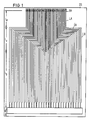
- the reference symbol DS denotes a thin film substrate on which the individual heating elements RH and their supply lines are structured. These supply lines - one forward and one return line per heating element - lead from the heating elements RH located in an edge region of the thin film substrate DS to a connection field AF located on the opposite side of the thin film substrate DS, where the supply lines are contacted to a connecting cable, not shown here. Since on the one hand there must be sufficient space for this contacting and on the other hand the heating elements RH should be arranged relatively small and closely adjacent due to the highest possible resolving power, the conductor tracks on the thin film substrate DS are fanned out.
- the conductor tracks on the thin-film substrate DS in the area of the heating elements RH are divided into conductor tracks of narrow pitch LA and in the area of the connection field AF in conductor tracks further pitch LB.
- a transition structure ÜV connects the interconnects narrow division LA with the conductors further division LB. The lengths of these three areas are also shown in FIG 1 A is the guide length of narrow pitch, 1 V is the length of the transition structure and 1 B is the length of the wire pitch.
- this transition structure ÜV which connects the conductor tracks of narrow division (in the area of the heating elements) with the conductor tracks of further division (in the area of the connection field), an identical and yet small lead resistance can be achieved for all heating dots.
- FIG. 2 shows an enlarged section from FIG. 1 and shows the course of two adjacent conductor tracks L1, L2 in the three areas mentioned.
- the geometric dimensions and the resistance contributions of the individual conductor track sections are shown in FIG. Specifically, these are the width d a , d v and d b of the conductor tracks in the areas of narrow pitch LA, the transition structure ÜV and further pitch LB and the distances s a , s v , s b of two adjacent conductor tracks L1, L2 in the corresponding areas.
- the conductor tracks within the individual areas run parallel to one another, while the conductor tracks of adjacent areas are arranged at right angles to one another.
- the total resistance of a conductor track L i is composed of a resistance component R bi of the conductor track of further division, a resistance component R vi of the transition structure and a resistance component R ai of the conductor joint of narrow division.
- This distance s v is a function of the predetermined parameters distances a , s b and conductor widths d a , d b of the conductor paths in the areas of narrow and wide division and the parameter conductor width d v in the transition area.
- abbreviation c d b ⁇ D a ⁇ (I.e.
- the equation (*) is shown in general form (s v , d v in the units ⁇ c).
- the trace width d v is plotted on the abscissa and the gap width s v on the ordinate.
- the resistance of a supply line R g is made up proportionally of the resistance contributions of the ladder narrow division LA, further division LB and the transition structure ÜV.
- Another example is a print head with a resolution of 300 dpi and 50 heating elements, the external dimensions of which are identical to the dimensions of the print head described above (180 dpi).
Landscapes
- Engineering & Computer Science (AREA)
- Manufacturing & Machinery (AREA)
- Microelectronics & Electronic Packaging (AREA)
- Particle Formation And Scattering Control In Inkjet Printers (AREA)
- Ink Jet (AREA)
- Parts Printed On Printed Circuit Boards (AREA)
- Structure Of Printed Boards (AREA)
Abstract
Claims (4)
- Procédé pour optimiser un dispositif de pistes conductrices pour une tête d'écriture dans des dispositifs d'impression à encre, dans lesquels une pluralité d'éléments de chauffage (RH) sont amorcés sélectivement par l'intermédiaire de pistes conductrices (Li) et ces pistes conductrices (Li) mènent séparément, sur un substrat à couche mince (DS), à un champ de raccord (AF), les pistes conductrices (Li) étant divisées en une zone de séparation étroite (LA) et en une zone de séparation large (LB) reliées au moyen d'une structure de jonction (UV),
caractérisé en ce que, à partir des tailles prédéfinies de structure des deux zones de pistes conductrices à relier, à savoir les largeurs de piste conductrice (da,db) et les largeurs d'espacement (Sa,Sb), ainsi qu'à partir de la largeur d'espacement (Sv) dans la structure de jonction (UV), la largeur de piste conductrice (dv) dans la structure de jonction (UV) est définie par la relation suivante :
de sorte que toutes les pistes conductrices (Li), présentent, pour les différents éléments de chauffage (RH), environ la même résistance. - Dispositif de pistes conductrices pour une tête d'écriture dans des dispositifs d'impression à encre, dans lesquels une pluralité d'éléments de chauffage (RH) sont amorcés sélectivement par l'intermédiaire de pistes conductrices (Li) et ces pistes conductrices (Li) mènent séparément, sur un substrat à couche mince (DS), à un champ de raccord (AF), les pistes conductrices (Li) s'étendant, à partir des éléments de chauffage (RH) à mettre en contact, dans une zone de séparation étroite (LA) des pistes conductrices, une zone de séparation large (LB) des pistes conductrices adjacente au champ de raccord (AF), et une structure de jonction (UV) reliant ces deux zones,
caractérisé en ce que les largeurs (di) des pistes conductrices (Li) et les écarts (largeurs d'espacement Si) entre deux pistes conductrices voisines (L1,L2) à l'intérieur de chacune des zones (LA,LB,UV) sont constantes et différentes par rapport aux autres zones (LA,LB,UV), en ce que, en fonction des largeurs de piste conductrice (da,db) et des largeurs d'espacement (Sa,Sb) des pistes conductrices (Li) dans les zones (LA,LB) ainsi que de la largeur d'espacement (Sv) dans la structure de jonction (UV), la largeur de piste conductrice (dv) dans la structure de jonction (UV) est dimensionnée de sorte que toutes les pistes conductrices présentent environ la même résistance (Rg). - Dispositif de pistes conductrices selon la revendication 2,
caractérisé en ce que les pistes conductrices (Li) s'étendent parallèlement les unes aux autres à l'intérieur des zones individuelles (LA,LB,UV). - Dispositif de pistes conductrices selon la revendication 2,
caractérisé en ce que, à chaque fois, les pistes conductrices de zones adjacentes (LA,UV,LB) sont agencées les unes par rapport aux autres à angle droit.
Applications Claiming Priority (2)
| Application Number | Priority Date | Filing Date | Title |
|---|---|---|---|
| EP88120855 | 1988-12-14 | ||
| EP88120855 | 1988-12-14 |
Publications (2)
| Publication Number | Publication Date |
|---|---|
| EP0448614A1 EP0448614A1 (fr) | 1991-10-02 |
| EP0448614B1 true EP0448614B1 (fr) | 1993-06-09 |
Family
ID=8199661
Family Applications (1)
| Application Number | Title | Priority Date | Filing Date |
|---|---|---|---|
| EP19900900866 Expired - Lifetime EP0448614B1 (fr) | 1988-12-14 | 1989-12-12 | Procede pour l'optimisation d'une configuration de traces conducteurs pour tete d'ecriture dans des imprimantes a jet d'encre et configuration de traces conducteurs pour ladite tete d'ecriture |
Country Status (4)
| Country | Link |
|---|---|
| EP (1) | EP0448614B1 (fr) |
| JP (1) | JPH04506187A (fr) |
| DE (1) | DE58904667D1 (fr) |
| WO (1) | WO1990006853A1 (fr) |
Families Citing this family (3)
| Publication number | Priority date | Publication date | Assignee | Title |
|---|---|---|---|---|
| DE4024545A1 (de) * | 1990-08-02 | 1992-02-06 | Boehringer Mannheim Gmbh | Verfahren und vorrichtung zum dosierten zufuehren einer biochemischen analysefluessigkeit auf ein target |
| US6398347B1 (en) * | 2000-07-24 | 2002-06-04 | Hewlett-Packard Company | Energy balanced ink jet printhead |
| JP2021174849A (ja) * | 2020-04-23 | 2021-11-01 | イビデン株式会社 | 配線基板 |
Family Cites Families (1)
| Publication number | Priority date | Publication date | Assignee | Title |
|---|---|---|---|---|
| US4612554A (en) * | 1985-07-29 | 1986-09-16 | Xerox Corporation | High density thermal ink jet printhead |
-
1989
- 1989-12-12 DE DE9090900866T patent/DE58904667D1/de not_active Expired - Fee Related
- 1989-12-12 EP EP19900900866 patent/EP0448614B1/fr not_active Expired - Lifetime
- 1989-12-12 JP JP2501461A patent/JPH04506187A/ja active Pending
- 1989-12-12 WO PCT/EP1989/001526 patent/WO1990006853A1/fr not_active Ceased
Also Published As
| Publication number | Publication date |
|---|---|
| DE58904667D1 (de) | 1993-07-15 |
| EP0448614A1 (fr) | 1991-10-02 |
| JPH04506187A (ja) | 1992-10-29 |
| WO1990006853A1 (fr) | 1990-06-28 |
Similar Documents
| Publication | Publication Date | Title |
|---|---|---|
| DE68913012T2 (de) | Thermischer Farbstrahldrucker mit mehrstufigen Durchschaltungen in den Druckkopfwandlern. | |
| DE69011647T2 (de) | Tintenstrahlkopf, sein Herstellungsverfahren, Substrat für einen Tintenstrahlkopf, Kontrollmethode hierzu und Tintenstrahlgerät. | |
| DE3008487C2 (fr) | ||
| DE60127761T2 (de) | Elektrodenstruktur einer Anzeigetafel und Verfahren zur Herstellung von Elektroden | |
| DE3610821C2 (fr) | ||
| DE60131855T2 (de) | Schmaler mehrfarbendruckkopf zum tintenstrahldrucken | |
| DE69408232T2 (de) | Selbstausrichtende Düsenkonstruktion für Thermo-Tintenstrahldruckköpfe | |
| DE3536370C2 (fr) | ||
| DE2840279C2 (de) | Tintenstrahldrucker | |
| DE4224345A1 (de) | Thermo-kopf | |
| DE3027911A1 (de) | Punktschreibkopf fuer praezisionsdrucker und verfahren zur herstellung desselben | |
| DE69825324T2 (de) | Thermokopf und thermodrucker | |
| EP0448614B1 (fr) | Procede pour l'optimisation d'une configuration de traces conducteurs pour tete d'ecriture dans des imprimantes a jet d'encre et configuration de traces conducteurs pour ladite tete d'ecriture | |
| DE69514610T2 (de) | Struktur einer Antriebsplatte für ein Tintenausstossgerät | |
| DE69705132T2 (de) | Thermischer Tintenstrahldrucker und Ansteuerungsverfahren | |
| DE69512887T2 (de) | Thermodruckkopf mit steuerschaltung und steueranordnung für thermodruckkopf | |
| EP0177633B1 (fr) | Enregistreur sur feuilles électrothermique | |
| DE19709344A1 (de) | Verfahren und Vorrichtung zum Erzielen gleichmäßiger Druckergebnisse unter Verwendung schmaler Druckkopfsegmente bei digitalen Druckern | |
| DE2852353A1 (de) | Elektrostatischer druckkopf | |
| DE69305398T2 (de) | Geteilter Thermo-Druckkopf | |
| DE4201633C2 (de) | Thermischer Druckkopf | |
| DE2852352C2 (de) | Elektrostatischer Druckkopf | |
| DE2810800C2 (de) | Mehrschichtige gedruckte Schaltung | |
| DE69030054T2 (de) | Thermo-Kopf | |
| DE2809615A1 (de) | Thermo-druckvorrichtung |
Legal Events
| Date | Code | Title | Description |
|---|---|---|---|
| PUAI | Public reference made under article 153(3) epc to a published international application that has entered the european phase |
Free format text: ORIGINAL CODE: 0009012 |
|
| 17P | Request for examination filed |
Effective date: 19910527 |
|
| AK | Designated contracting states |
Kind code of ref document: A1 Designated state(s): DE |
|
| 17Q | First examination report despatched |
Effective date: 19920622 |
|
| GRAA | (expected) grant |
Free format text: ORIGINAL CODE: 0009210 |
|
| AK | Designated contracting states |
Kind code of ref document: B1 Designated state(s): DE |
|
| REF | Corresponds to: |
Ref document number: 58904667 Country of ref document: DE Date of ref document: 19930715 |
|
| PGFP | Annual fee paid to national office [announced via postgrant information from national office to epo] |
Ref country code: DE Payment date: 19931227 Year of fee payment: 5 |
|
| PLBE | No opposition filed within time limit |
Free format text: ORIGINAL CODE: 0009261 |
|
| STAA | Information on the status of an ep patent application or granted ep patent |
Free format text: STATUS: NO OPPOSITION FILED WITHIN TIME LIMIT |
|
| 26N | No opposition filed | ||
| PG25 | Lapsed in a contracting state [announced via postgrant information from national office to epo] |
Ref country code: DE Effective date: 19950901 |