EP0448692B1 - Méthode de formation une couche de semiconductrice monocristallin sur un substrat non-monocristallin - Google Patents
Méthode de formation une couche de semiconductrice monocristallin sur un substrat non-monocristallin Download PDFInfo
- Publication number
- EP0448692B1 EP0448692B1 EP90915698A EP90915698A EP0448692B1 EP 0448692 B1 EP0448692 B1 EP 0448692B1 EP 90915698 A EP90915698 A EP 90915698A EP 90915698 A EP90915698 A EP 90915698A EP 0448692 B1 EP0448692 B1 EP 0448692B1
- Authority
- EP
- European Patent Office
- Prior art keywords
- layer
- monocrystalline
- forming
- substrate
- regions
- Prior art date
- Legal status (The legal status is an assumption and is not a legal conclusion. Google has not performed a legal analysis and makes no representation as to the accuracy of the status listed.)
- Expired - Lifetime
Links
Images



Classifications
-
- H—ELECTRICITY
- H10—SEMICONDUCTOR DEVICES; ELECTRIC SOLID-STATE DEVICES NOT OTHERWISE PROVIDED FOR
- H10F—INORGANIC SEMICONDUCTOR DEVICES SENSITIVE TO INFRARED RADIATION, LIGHT, ELECTROMAGNETIC RADIATION OF SHORTER WAVELENGTH OR CORPUSCULAR RADIATION
- H10F71/00—Manufacture or treatment of devices covered by this subclass
- H10F71/125—The active layers comprising only Group II-VI materials, e.g. CdS, ZnS or CdTe
- H10F71/1253—The active layers comprising only Group II-VI materials, e.g. CdS, ZnS or CdTe comprising at least three elements, e.g. HgCdTe
-
- H—ELECTRICITY
- H10—SEMICONDUCTOR DEVICES; ELECTRIC SOLID-STATE DEVICES NOT OTHERWISE PROVIDED FOR
- H10F—INORGANIC SEMICONDUCTOR DEVICES SENSITIVE TO INFRARED RADIATION, LIGHT, ELECTROMAGNETIC RADIATION OF SHORTER WAVELENGTH OR CORPUSCULAR RADIATION
- H10F30/00—Individual radiation-sensitive semiconductor devices in which radiation controls the flow of current through the devices, e.g. photodetectors
- H10F30/20—Individual radiation-sensitive semiconductor devices in which radiation controls the flow of current through the devices, e.g. photodetectors the devices having potential barriers, e.g. phototransistors
- H10F30/21—Individual radiation-sensitive semiconductor devices in which radiation controls the flow of current through the devices, e.g. photodetectors the devices having potential barriers, e.g. phototransistors the devices being sensitive to infrared, visible or ultraviolet radiation
- H10F30/22—Individual radiation-sensitive semiconductor devices in which radiation controls the flow of current through the devices, e.g. photodetectors the devices having potential barriers, e.g. phototransistors the devices being sensitive to infrared, visible or ultraviolet radiation the devices having only one potential barrier, e.g. photodiodes
- H10F30/221—Individual radiation-sensitive semiconductor devices in which radiation controls the flow of current through the devices, e.g. photodetectors the devices having potential barriers, e.g. phototransistors the devices being sensitive to infrared, visible or ultraviolet radiation the devices having only one potential barrier, e.g. photodiodes the potential barrier being a PN homojunction
- H10F30/2212—Individual radiation-sensitive semiconductor devices in which radiation controls the flow of current through the devices, e.g. photodetectors the devices having potential barriers, e.g. phototransistors the devices being sensitive to infrared, visible or ultraviolet radiation the devices having only one potential barrier, e.g. photodiodes the potential barrier being a PN homojunction the devices comprising active layers made of only Group II-VI materials, e.g. HgCdTe infrared photodiodes
-
- H—ELECTRICITY
- H10—SEMICONDUCTOR DEVICES; ELECTRIC SOLID-STATE DEVICES NOT OTHERWISE PROVIDED FOR
- H10F—INORGANIC SEMICONDUCTOR DEVICES SENSITIVE TO INFRARED RADIATION, LIGHT, ELECTROMAGNETIC RADIATION OF SHORTER WAVELENGTH OR CORPUSCULAR RADIATION
- H10F39/00—Integrated devices, or assemblies of multiple devices, comprising at least one element covered by group H10F30/00, e.g. radiation detectors comprising photodiode arrays
- H10F39/10—Integrated devices
- H10F39/107—Integrated devices having multiple elements covered by H10F30/00 in a repetitive configuration, e.g. radiation detectors comprising photodiode arrays
-
- H—ELECTRICITY
- H10—SEMICONDUCTOR DEVICES; ELECTRIC SOLID-STATE DEVICES NOT OTHERWISE PROVIDED FOR
- H10F—INORGANIC SEMICONDUCTOR DEVICES SENSITIVE TO INFRARED RADIATION, LIGHT, ELECTROMAGNETIC RADIATION OF SHORTER WAVELENGTH OR CORPUSCULAR RADIATION
- H10F77/00—Constructional details of devices covered by this subclass
- H10F77/10—Semiconductor bodies
- H10F77/16—Material structures, e.g. crystalline structures, film structures or crystal plane orientations
- H10F77/162—Non-monocrystalline materials, e.g. semiconductor particles embedded in insulating materials
- H10F77/164—Polycrystalline semiconductors
-
- H—ELECTRICITY
- H10—SEMICONDUCTOR DEVICES; ELECTRIC SOLID-STATE DEVICES NOT OTHERWISE PROVIDED FOR
- H10P—GENERIC PROCESSES OR APPARATUS FOR THE MANUFACTURE OR TREATMENT OF DEVICES COVERED BY CLASS H10
- H10P14/00—Formation of materials, e.g. in the shape of layers or pillars
- H10P14/20—Formation of materials, e.g. in the shape of layers or pillars of semiconductor materials
- H10P14/27—Formation of materials, e.g. in the shape of layers or pillars of semiconductor materials using selective deposition, e.g. simultaneous growth of monocrystalline and non-monocrystalline semiconductor materials
- H10P14/271—Formation of materials, e.g. in the shape of layers or pillars of semiconductor materials using selective deposition, e.g. simultaneous growth of monocrystalline and non-monocrystalline semiconductor materials characterised by the preparation of substrate for selective deposition
-
- H—ELECTRICITY
- H10—SEMICONDUCTOR DEVICES; ELECTRIC SOLID-STATE DEVICES NOT OTHERWISE PROVIDED FOR
- H10P—GENERIC PROCESSES OR APPARATUS FOR THE MANUFACTURE OR TREATMENT OF DEVICES COVERED BY CLASS H10
- H10P14/00—Formation of materials, e.g. in the shape of layers or pillars
- H10P14/20—Formation of materials, e.g. in the shape of layers or pillars of semiconductor materials
- H10P14/27—Formation of materials, e.g. in the shape of layers or pillars of semiconductor materials using selective deposition, e.g. simultaneous growth of monocrystalline and non-monocrystalline semiconductor materials
- H10P14/271—Formation of materials, e.g. in the shape of layers or pillars of semiconductor materials using selective deposition, e.g. simultaneous growth of monocrystalline and non-monocrystalline semiconductor materials characterised by the preparation of substrate for selective deposition
- H10P14/274—Formation of materials, e.g. in the shape of layers or pillars of semiconductor materials using selective deposition, e.g. simultaneous growth of monocrystalline and non-monocrystalline semiconductor materials characterised by the preparation of substrate for selective deposition using seed materials
-
- H—ELECTRICITY
- H10—SEMICONDUCTOR DEVICES; ELECTRIC SOLID-STATE DEVICES NOT OTHERWISE PROVIDED FOR
- H10P—GENERIC PROCESSES OR APPARATUS FOR THE MANUFACTURE OR TREATMENT OF DEVICES COVERED BY CLASS H10
- H10P14/00—Formation of materials, e.g. in the shape of layers or pillars
- H10P14/20—Formation of materials, e.g. in the shape of layers or pillars of semiconductor materials
- H10P14/29—Formation of materials, e.g. in the shape of layers or pillars of semiconductor materials characterised by the substrates
- H10P14/2901—Materials
- H10P14/2921—Materials being crystalline insulating materials
-
- H—ELECTRICITY
- H10—SEMICONDUCTOR DEVICES; ELECTRIC SOLID-STATE DEVICES NOT OTHERWISE PROVIDED FOR
- H10P—GENERIC PROCESSES OR APPARATUS FOR THE MANUFACTURE OR TREATMENT OF DEVICES COVERED BY CLASS H10
- H10P14/00—Formation of materials, e.g. in the shape of layers or pillars
- H10P14/20—Formation of materials, e.g. in the shape of layers or pillars of semiconductor materials
- H10P14/32—Formation of materials, e.g. in the shape of layers or pillars of semiconductor materials characterised by intermediate layers between substrates and deposited layers
- H10P14/3202—Materials thereof
- H10P14/3238—Materials thereof being insulating materials
-
- H—ELECTRICITY
- H10—SEMICONDUCTOR DEVICES; ELECTRIC SOLID-STATE DEVICES NOT OTHERWISE PROVIDED FOR
- H10P—GENERIC PROCESSES OR APPARATUS FOR THE MANUFACTURE OR TREATMENT OF DEVICES COVERED BY CLASS H10
- H10P14/00—Formation of materials, e.g. in the shape of layers or pillars
- H10P14/20—Formation of materials, e.g. in the shape of layers or pillars of semiconductor materials
- H10P14/34—Deposited materials, e.g. layers
- H10P14/3402—Deposited materials, e.g. layers characterised by the chemical composition
- H10P14/3424—Deposited materials, e.g. layers characterised by the chemical composition being Group IIB-VIA materials
- H10P14/3432—Tellurides
-
- Y—GENERAL TAGGING OF NEW TECHNOLOGICAL DEVELOPMENTS; GENERAL TAGGING OF CROSS-SECTIONAL TECHNOLOGIES SPANNING OVER SEVERAL SECTIONS OF THE IPC; TECHNICAL SUBJECTS COVERED BY FORMER USPC CROSS-REFERENCE ART COLLECTIONS [XRACs] AND DIGESTS
- Y02—TECHNOLOGIES OR APPLICATIONS FOR MITIGATION OR ADAPTATION AGAINST CLIMATE CHANGE
- Y02E—REDUCTION OF GREENHOUSE GAS [GHG] EMISSIONS, RELATED TO ENERGY GENERATION, TRANSMISSION OR DISTRIBUTION
- Y02E10/00—Energy generation through renewable energy sources
- Y02E10/50—Photovoltaic [PV] energy
-
- Y—GENERAL TAGGING OF NEW TECHNOLOGICAL DEVELOPMENTS; GENERAL TAGGING OF CROSS-SECTIONAL TECHNOLOGIES SPANNING OVER SEVERAL SECTIONS OF THE IPC; TECHNICAL SUBJECTS COVERED BY FORMER USPC CROSS-REFERENCE ART COLLECTIONS [XRACs] AND DIGESTS
- Y10—TECHNICAL SUBJECTS COVERED BY FORMER USPC
- Y10S—TECHNICAL SUBJECTS COVERED BY FORMER USPC CROSS-REFERENCE ART COLLECTIONS [XRACs] AND DIGESTS
- Y10S117/00—Single-crystal, oriented-crystal, and epitaxy growth processes; non-coating apparatus therefor
- Y10S117/913—Graphoepitaxy or surface modification to enhance epitaxy
Definitions
- the present invention relates to the method of forming a monocrystalline layer on a non-monocrystalline substrate. It is especially useful in the manufacture of integrated electronic element wafers for making a photosensitive detector array.
- the infrared spectrum covers a range of wavelengths longer than the visible wavelengths, but shorter than microwave wavelengths. Visible wavelengths are generally regarded as between 0.4 and 0.75 micrometers. The infrared wavelengths extend from 0.75 micrometers to 1 millimeter. The function of an infrared detector is to respond to the energy of a wavelength within some particular portion of the infrared region.
- Heated objects generate radiant energy having characteristic wavelengths within the infrared spectrum.
- Many current infrared image detection systems incorporate arrays with large numbers of discrete, highly sensitive detector elements, the electrical outputs of which are connected to processing circuitry. By analyzing the pattern and sequence of detector element excitations, the processing circuitry can identify and track sources of infrared radiation. Though the theoretical performance of such contemporary systems is satisfactory for many applications, it is difficult to construct structures that adequately interface large numbers of detector elements with associated signal processing circuitry in a practical and reliable manner.
- Contemporary arrays of detectors may be sized to include 256 detector elements on a side, or a total of 65,536 detectors, the size of each square detector being approximately 0.009 centimeters on a side, with 0.00127 centimeters spacing between detectors.
- Infrared detector arrays are commonly fabricated from single crystalline layers of an infrared radiation-absorbing material. Layer thicknesses of approximately ten microns are typical. These single crystalline layers are formed by epitaxial crystal growth upon a single crystalline wafer substrate. The substrate must have a closely matching crystal lattice structure to provide epitaxial layer growth. The substrate, which conventionally faces the infrared radiation, must then be transparent to those wavelengths of infrared radiation which are to be detected, i.e., from the surface of the detector in contact with the substrate. Such substrate-side irradiation is used because detector element electrodes and a conductive grid are fabricated upon the surface of the detector layer. The electrodes and conductive grid cannot be formed beneath the detector because a continuous single crystalline substrate surface is required for epitaxial growth.
- HgCdTe Mercury cadmium telluride
- An epitaxial layer of HgCdTe can be grown upon cadmium telluride (CdTe) or upon CdTe on sapphire or on gallium arsenide (GaAs). It is difficult to obtain a CdTe wafer or layer substrate that results in a high performance HgCdTe detector array.
- the present invention is in a method as defined in Claim 1.
- EP-A-0297559 of a photosensor including a light-absorbing layer formed by growing graphotaxially from a seed crystal of the same material: this has the features of the pre-characterising portion of Claim 1.
- EP-A-0284441 discloses a method of forming a monocrystalline seed in a cavity in a glass layer and allowing it to grow to fill the cavity.
- Graphotaxy is the growth of a single crystalline layer across the surface of a non-single crystalline substrate by commencing growth at a single-crystalline seed surface.
- this surface is provided by a seed crystal that is placed upon the non-single crystalline substrate.
- the seed crystal surface is the same material as the material to be grown. Growth takes place layer-by-layer on this surface. When it reaches the non-crystalline substrate surface, it spreads laterally across this surface.
- the seed establishes the crystalline structure and orientation of the graphotaxially grown layer. Once established, the structure and orientation are maintained since all growth originates from the same single-crystalline seed.
- That process is contrasted to conventional epitaxial growth where the crystal is grown on the surface of a single crystalline substrate.
- epitaxial growth the entire surface of the substrate serves as a seed and must therefore be single crystalline to maintain single crystalline growth.
- the substrate can be entirely different in chemical composition from the grown layers, so long as there is a close match in the crystal lattice.
- a seed crystal of the material which will comprise the layer to be grown is embedded in the substrate. Growth occurs layer-by-layer on the seed crystal and travels across the surface of the substrate.
- the glass softening involves liquefying and glazing the glass layer so as to cause the seed crystal to sink into and be sealed by the glass layer.
- the material to be grown can be supplied as a vapor or liquid.
- vias, electrodes and a grid are formed upon the glassified surface of the substrate prior to graphotaxial growth.
- Regions of material of a second type e.g. n-type
- p-type the material of a first type in the regions of the electrodes as one means to create detector element p-n junctions.
- Another means is to grow a layer of the second type epitaxially over the first layer.
- Graphotaxial growth of a single crystalline layer upon polycrystalline or amorphous substrates permits the use of a much thicker substrate which will withstand the many steps of the wafer fabrication process.
- infrared opaque materials can be employed as the wafer substrate since substrate-side illumination of the detector is not required.
- Substrate-side illumination is not required because the photosensitive layer is grown graphotaxially over electrodes and a grid which are formed upon the substrate. Therefore, substrate preparation is minimal. Electrodes and a grid are patterned upon an insulator substrate surface before epitaxial crystal growth. Vias can be easily formed in the substrate to enable electrical contacts, bonds or leads to be conveniently located on the reverse side of the substrate.
- a wafer 10 has a glass layer 12 is deposited upon a substrate 14, such as an alumina ceramic material.
- a seed crystal 16 is placed upon the glass layer 12.
- the seed crystal 16 is comprised of a single crystalline material surface of a first type, e.g., a p-type semiconductor such as a p-HgCdTe..
- the wafer 10 is heated to a temperature sufficient to liquify and glaze the glass layer 12 so as to cause the seed crystal to be sealed in the glass layer 12.
- apertures or vias 18 may be formed through the substrate 10 and glass layer 12. Vias 18 extend through the glass layer 12 and the substrate 14 such that they provide a continuous electrically conductive passage from the upper surface of the wafer 10 to the lower surface of the wafer 10, where contacts, bonds or leads can subsequently be formed.
- a metal film is deposited upon the glass layer 12 to form electrodes 20 and a conductive grid 22.
- Each of the electrodes 20 may be formed directly over a via 18 so as to provide convenient electrical connection from the electrode 20 to the lower surface of the wafer 10.
- the conductive grid 22 forms a common electrode for all detectors and may likewise be connected to the lower surface of the wafer 10 with a via 18.
- a layer 24 of the seed material of the first type is graphotaxially grown across the surface of the glass layer 12 by either liquid epitaxy or vapor phase epitaxy. That is, the techniques of liquid epitaxy or vapor phase epitaxy are used upon the wafer formed as described above to supply the materials for graphotaxial crystal growth.
- regions of the layer 24 of material of a first type must be modified to become a material of the second type, i.e., an n-type semiconductor, in the vicinity of the electrodes 20 to form detector element p-n junctions.
- this is accomplished by masked, deep ion implantation that results in the formation of a region 26 of material of a second type in the vicinity of the electrodes 20.
- a p-type layer can be modified to become an n-type layer by boron implantation.
- the regions of material of a second type can be formed by counterdoping the layer by diffusion from the electrode material. If electrode material diffusion is used to modify the material of a first type to a material of the second type then the grid material must be different from the electrode material, such that the grid material does not diffuse to form a material of the second type as does the electrode material. Further, the softening temperature of the glass layer must be greater than the diffusion temperature of the electrode material.
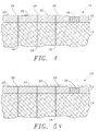
- a further alternative is to form a second layer 25 epitaxially upon the first layer 24 in order to form the p-n junctions.
- the first layer 24 can be graphotaxially grown as described above and then ion implanted for a type conversion in the material of the first type in the region 28 covering the electrodes 20.
- a second layer 25 of material of the first type is then grown epitaxially over the first layer, which is now comprised of regions of material of the first type 24 and regions of material of the second type 28. Deep ion implantation is not required since the first layer can be converted completely from top to bottom. This is possible because a second layer 25 of material of the first type is being added over top of the first layer to form the p-n junctions.
- the p-n junctions can also be formed by growing the first layer such that it is patterned to be limited to the regions 24 that cover the electrodes 20 only.
- the first layer is removed from the area of the grid 22.
- the first layer may then be ion implanted to convert it to a material of a second type or remain of a first type.
- a second layer comprising material of the opposite type is then grown by conventional epitaxy over the first layer comprised of regions 24.
- the second layer would then comprise region 25 covering the grid 22, layer 24 and the remainder of the surface of the wafer 10.
- the second layer 25 may be prone to defects, since each first layer region 24 can be a seed for crystal growth.
- the second layer can be formed free of defects at the p-n junctions, since crystal growth begins at the p-n junctions and the defects do not occur until further growth proceeds.
- the seed crystal region and individual detector arrays of a desired dimension are cut from the wafer.
- a second method for forming the single crystalline seed material for graphotaxial growth upon a non-single crystalline substrate is disclosed.
- a first layer of seed material is graphotaxially grown upon a first substrate as given in the previous method.
- the first substrate upon which the first layer of seed material is graphotaxially grown is cut to form chips, each of which comprise a portion of the first substrate and a portion of the first layer.
- These seed chips designated generally in Figures 8 and 9 as 30, are embedded in a cavity 40 formed in a second substrate 34.
- the first or chip substrate is designated 36 and the single crystalline layer is designated 38.
- the second substrate 34 has a glass layer 32 formed upon its upper surface. The height of the upper surface of the seed chip 30 is below the level of the upper surface of the glass coating 32.
- the upper surface of the seed crystal 30 is preferably made lower than the upper surface of the glass coating 32 by forming the seed crystal 30 such that its height is less than the height of the substrate 34 plus the thickness of the glass layer 32.
- a shim 42 can be formed upon the lower surface of the substrate 34. Such a shim 42 is required when the thickness of the seed crystal 30 is approximately equal to or greater than the thickness of the substrate 34 plus the thickness of the glass layer 32.
- the shim 42 can be formed of gold.
- the gold shim 42 can be deposited upon the lower surface of the substrate 34 by electroplating to the desired thickness. Electroplating permits very close control of the shim thickness, thereby enabling the seed chip 30 to have its upper surface positioned precisely below the upper surface of the substrate 34.
- the melting temperature of gold is high enough to withstand the glassification of the glass layer 32 and gold can be removed chemically at a later point in the wafer -fabrication process if desired.
Landscapes
- Light Receiving Elements (AREA)
- Recrystallisation Techniques (AREA)
Abstract
Claims (26)
- Méthode de formation d'une couche monocristalline de matériau semi-conducteur sur un substrat non monocristallin, comprenant les étapes de :a) dépôt d'une couche de verre (12) sur ledit substrat non monocristallin (14) ;b) croissance de manière graphotaxiale d'une première couche monocristalline (24) dudit matériau semi-conducteur, qui a un premier type de conductivité, sur la face exposée de ladite couché de verre à partir d'un cristal germe (16) ayant une surface monocristalline dudit matériau semi-conducteur, du premier type de conductivité;caractérisée en ce que, entre les étapes a) et b), ledit cristal germe est placé sur ladite couche de verre, et que ladite couche de verre est liquéfiée par réchauffement afin que ledit cristal germe pénètre et soit scellé dans la couche de verre dans laquelle il est noyé pendant que ladite surface monocristalline dudit cristal germe reste exposée.
- Méthode selon la revendication 1, dans laquelle ledit substrat non monocristallin (14) est une céramique d'alumine et ledit matériau semi-conducteur est un HgCdTe.
- Méthode selon la revendication 2, comprenant en outre une étape de formation de voies (18) à travers ledit substrat non monocristallin (14).
- Méthode selon la revendication 3, comprenant en outre une étape de dépôt d'un film métallique (20, 22) sur ladite couche de verre pour former des électrodes et une grille conductrice avant l'étape b).
- Méthode selon la revendication 4, dans laquelle ladite première couche monocristalline croît de manière graphotaxiale par le procédé d'épitaxie en phase liquide.
- Méthode selon la revendication 4, dans laquelle ladite première couche monocristalline croît de manière graphotaxiale par le procédé d'épitaxie en phase gazeuse.
- Méthode selon la revendication 4, comprenant en outre une étape de formation de régions d'un second type de conductivité du matériau semi-conducteur monocristallin, pour créer des jonctions p-n, lesdites régions étant sensiblement au-dessus desdites électrodes.
- Méthode selon la revendication 7, dans laquelle ladite étape de formation desdites régions comprend le procédé d'implantation ionique profonde masquée.
- Méthode selon la revendication 7, dans laquelle ladite étape de formation desdites régions comprend le procédé de contre-dopage par diffusion à partir du matériau des électrodes.
- Méthode selon la revendication 7, dans laquelle ladite étape de formation desdites régions comprend le procédé d'implantation ionique de ladite première couche monocristalline pour former lesdites régions et le développement d'une seconde couche monocristalline (25) dudit matériau semi-conducteur d'un premier type de conductivité sur ladite première couche monocristalline (24), y compris lesdites régions dudit second type de conductivité.
- Méthode selon la revendication 7, dans laquelle ladite étape de formation desdites régions comprend la structuration de ladite première couche monocristalline (24, figure 7b) de façon à ce que seules restent les régions de ladite première couche monocristalline sensiblement disposée sur lesdites électrodes (20), puis la formation d'une seconde couche monocristalline dudit matériau semi-conducteur dudit second type de conductivité, sur sensiblement la totalité de la surface dudit substrat non monocristallin.
- Méthode selon la revendication 7, comprenant en outre une étape de formation de voies conductrices s'étendant des électrodes à travers ladite couche de verre et ledit substrat non monocristallin.
- Méthode de formation d'une couche monocristalline de matériau semi-conducteur sur un substrat non monocristallin, comprenant les étapes de :a) formation de puces germes (30) par le découpage de la structure obtenue par la méthode selon la revendication 1 ;b) encastrement d'une desdites puces germes dans une ouverture (40) formée dans un second substrat non monocristallin dont la face supérieure est sensiblement recouverte par une seconde couche de verre (32), par laquelle la surface exposée de ladite première couche monocristalline d'une desdites puces germes est en dessous de la surface exposée de ladite seconde couche de verre ;c) croissance de manière graphotaxiale d'une autre couche monocristalline (24) dudit matériau semi-conducteur depuis la surface exposée de ladite puce germe, ayant d'abord un type de conductivité à partir de la surface exposée de laddite puce germe, à travers la surface exposée de ladite seconde couche de verre.
- Méthode selon la revendication 13, dans laquelle ledit matériau semi-conducteur est du HgCdTe et ledit second substrat non monocristallin (34) est une céramique d'alumine.
- Méthode selon la revendication 14, comprenant en outre une étape de formation de voies à travers ledit substrat non monocristallin.
- Méthode selon la revendication 15, comprenant en outre une étape de dépôt d'un film métallique sur ladite seconde couche de verre (32) pour former des électrodes et une grille conductrice avant l'étape c).
- Méthode selon la revendication 16, -dans laquelle ladite couche monocristalline additionnelle croît par le procédé d'épitaxie en phase liquide.
- Méthode selon la revendication 16, dans laquelle ladite couche monocristalline additionnelle croît par le procédé d'épitaxie en phase gazeuse.
- Méthode selon la revendication 16, comprenant en outre une autre étape de formation de régions du second type de conductivité du matériau semi-conducteur monocristallin, pour créer des jonctions p-n, lesdites régions étant sensiblement au-dessus desdites électrodes.
- Méthode selon la revendication 19, dans laquelle ladite étape de formation desdites régions comprend le procédé d'implantation ionique profonde masquée.
- Méthode selon la revendication 19, dans laquelle ladite étape de formation desdites régions comprend le procédé de contre-dopage de la couche par diffusion à partir du matériau des électrodes.
- Méthode selon la revendication 19, dans laquelle ladite étape de formation desdites régions comprend le procédé d'implantation ionique de ladite couche monocristalline additionnelle pour former lesdites régions et la croissance d'une seconde couche monocristalline additionnelle (25) dudit matériau semi-conducteur du premier type de conductivité sur ladite couche monocristalline additionnelle (24) y compris lesdites régions du second type de conductivité.
- Méthode selon la revendication 19, dans laquelle ladite étape de formation desdites régions comprend le procédé de structuration de ladite couche monocristalline additionnelle, de façon à ce que seules restent les régions de ladite couche monocristalline additionnelle située sur lesdites électrodes (20), puis la formation d'une seconde couche monocristalline additionnelle dudit matériau semi-conducteur dudit second type de conductivité sur sensiblement la totalité de la surface dudit substrat non monocristallin.
- Méthode selon la revendication 13, dans laquelle lesdites puces germes sont plus minces que la hauteur dudit second substrat non monocristallin (34) y compris ladite seconde couche de verre.
- Méthode selon la revendication 13, dans laquelle lesdites puces germes (30) sont plus épaisses que la hauteur dudit second substrat non monocristallin y compris ladite seconde couche de verre, et dans laquelle une cale (42) est formée sur la face inférieure dudit second substrat non monocristallin pour augmenter sa hauteur.
- Méthode décrite dans la revendication 25, dans laquelle ladite cale est en or.
Applications Claiming Priority (3)
| Application Number | Priority Date | Filing Date | Title |
|---|---|---|---|
| US07/419,211 US4988641A (en) | 1989-10-10 | 1989-10-10 | Graphotaxially forming a photosensitive detector array |
| PCT/US1990/005748 WO1991006127A1 (fr) | 1989-10-10 | 1990-10-09 | Reseau de detecteurs photosensibles formes graphotaxialement |
| US419211 | 1999-10-15 |
Publications (3)
| Publication Number | Publication Date |
|---|---|
| EP0448692A1 EP0448692A1 (fr) | 1991-10-02 |
| EP0448692A4 EP0448692A4 (en) | 1992-07-01 |
| EP0448692B1 true EP0448692B1 (fr) | 1997-09-17 |
Family
ID=23661274
Family Applications (1)
| Application Number | Title | Priority Date | Filing Date |
|---|---|---|---|
| EP90915698A Expired - Lifetime EP0448692B1 (fr) | 1989-10-10 | 1990-10-09 | Méthode de formation une couche de semiconductrice monocristallin sur un substrat non-monocristallin |
Country Status (5)
| Country | Link |
|---|---|
| US (1) | US4988641A (fr) |
| EP (1) | EP0448692B1 (fr) |
| JP (1) | JPH04502237A (fr) |
| DE (1) | DE69031461T2 (fr) |
| WO (1) | WO1991006127A1 (fr) |
Families Citing this family (9)
| Publication number | Priority date | Publication date | Assignee | Title |
|---|---|---|---|---|
| JPH05121317A (ja) * | 1991-10-24 | 1993-05-18 | Rohm Co Ltd | Soi構造形成方法 |
| US5536948A (en) * | 1994-08-23 | 1996-07-16 | Grumman Aerospace Corporation | Infrared detector element substrate with superlattice layers |
| US5475224A (en) * | 1994-08-26 | 1995-12-12 | Grumman Aerospace Corporation | Infrared detector substrate with breakaway test tabs |
| US5599744A (en) * | 1995-02-06 | 1997-02-04 | Grumman Aerospace Corporation | Method of forming a microcircuit via interconnect |
| US5661267A (en) * | 1995-03-15 | 1997-08-26 | Northrop Grumman Corporation | Detector alignment board |
| US5621193A (en) * | 1995-05-23 | 1997-04-15 | Northrop Grumman Corporation | Ceramic edge connect process |
| JPH09205234A (ja) * | 1996-01-26 | 1997-08-05 | Nec Corp | 磁気抵抗効果素子及び磁気抵抗効果センサ |
| US8010174B2 (en) * | 2003-08-22 | 2011-08-30 | Dexcom, Inc. | Systems and methods for replacing signal artifacts in a glucose sensor data stream |
| WO2016069083A2 (fr) * | 2014-09-09 | 2016-05-06 | The University Of North Carolina At Charlotte | Détecteur optique basé sur une surface diélectrique à structure antiréfléchissante et sur un absorbeur métallique |
Citations (2)
| Publication number | Priority date | Publication date | Assignee | Title |
|---|---|---|---|---|
| EP0284441A2 (fr) * | 1987-03-26 | 1988-09-28 | Canon Kabushiki Kaisha | Produit cristallin composite du groupe II-VI et son procédé de fabrication |
| EP0297559A2 (fr) * | 1987-06-30 | 1989-01-04 | Canon Kabushiki Kaisha | Capteur de lumière |
Family Cites Families (27)
| Publication number | Priority date | Publication date | Assignee | Title |
|---|---|---|---|---|
| US3884788A (en) * | 1973-08-30 | 1975-05-20 | Honeywell Inc | Substrate preparation for liquid phase epitaxy of mercury cadmium telluride |
| US4727047A (en) * | 1980-04-10 | 1988-02-23 | Massachusetts Institute Of Technology | Method of producing sheets of crystalline material |
| NL8220051A (nl) * | 1981-02-04 | 1983-01-03 | Western Electric Co | Werkwijze voor het vormen van een monokristallijn halfgeleidergebied op een isolatiefilm. |
| US4371421A (en) * | 1981-04-16 | 1983-02-01 | Massachusetts Institute Of Technology | Lateral epitaxial growth by seeded solidification |
| US4596626A (en) * | 1983-02-10 | 1986-06-24 | The United States Of America As Represented By The United States National Aeronautics And Space Administration | Method of making macrocrystalline or single crystal semiconductor material |
| US4593456A (en) * | 1983-04-25 | 1986-06-10 | Rockwell International Corporation | Pyroelectric thermal detector array |
| US4672737A (en) * | 1984-01-23 | 1987-06-16 | Irvine Sensors Corporation | Detector array module fabrication process |
| US4564403A (en) * | 1984-01-27 | 1986-01-14 | Sony Corporation Research Center | Single-crystal semiconductor devices and method for making them |
| US4578142A (en) * | 1984-05-10 | 1986-03-25 | Rca Corporation | Method for growing monocrystalline silicon through mask layer |
| US4588447A (en) * | 1984-06-25 | 1986-05-13 | Rockwell International Corporation | Method of eliminating p-type electrical activity and increasing channel mobility of Si-implanted and recrystallized SOS films |
| JPS61121433A (ja) * | 1984-11-19 | 1986-06-09 | Sharp Corp | 半導体基板 |
| US4633086A (en) * | 1985-04-09 | 1986-12-30 | Grumman Aerospace Corporation | Input circuit for infrared detector |
| US4703170A (en) * | 1985-04-12 | 1987-10-27 | Grumman Aerospace Corporation | Infrared focal plane module |
| US4792672A (en) * | 1985-04-12 | 1988-12-20 | Grumman Aerospace Corporation | Detector buffer board |
| US4618763A (en) * | 1985-04-12 | 1986-10-21 | Grumman Aerospace Corporation | Infrared focal plane module with stacked IC module body |
| US4659931A (en) * | 1985-05-08 | 1987-04-21 | Grumman Aerospace Corporation | High density multi-layered integrated circuit package |
| US4618380A (en) * | 1985-06-18 | 1986-10-21 | The United States Of America As Represented By The Administrator Of The National Aeronautics And Space Administration | Method of fabricating an imaging X-ray spectrometer |
| DE3626504C2 (de) * | 1985-08-07 | 1996-06-27 | Sharp Kk | Verfahren zur Herstellung eines linearen Bildsensors |
| US4692610A (en) * | 1986-01-30 | 1987-09-08 | Grumman Aerospace Corporation | Fiber optic aircraft load relief control system |
| US4734577A (en) * | 1986-01-30 | 1988-03-29 | Grumman Aerospace Corporation | Continuous strain measurement along a span |
| US4718075A (en) * | 1986-03-28 | 1988-01-05 | Grumman Aerospace Corporation | Raster scan anode X-ray tube |
| US4698603A (en) * | 1986-05-05 | 1987-10-06 | Grumman Aerospace Corporation | RF amplitude modulator/mixer |
| FR2604298B1 (fr) * | 1986-09-19 | 1988-10-28 | Commissariat Energie Atomique | Procede de realisation d'une prise de contact electrique sur un substrat en hgcdte de conductivite p et application a la fabrication d'une diode n/p |
| US4852141A (en) * | 1987-08-03 | 1989-07-25 | Grumman Aerospace Corporation | Portable X-ray collimator and scatter shield |
| US4743567A (en) * | 1987-08-11 | 1988-05-10 | North American Philips Corp. | Method of forming thin, defect-free, monocrystalline layers of semiconductor materials on insulators |
| US4794092A (en) * | 1987-11-18 | 1988-12-27 | Grumman Aerospace Corporation | Single wafer moated process |
| US4784970A (en) * | 1987-11-18 | 1988-11-15 | Grumman Aerospace Corporation | Process for making a double wafer moated signal processor |
-
1989
- 1989-10-10 US US07/419,211 patent/US4988641A/en not_active Expired - Fee Related
-
1990
- 1990-10-09 WO PCT/US1990/005748 patent/WO1991006127A1/fr not_active Ceased
- 1990-10-09 DE DE69031461T patent/DE69031461T2/de not_active Expired - Fee Related
- 1990-10-09 EP EP90915698A patent/EP0448692B1/fr not_active Expired - Lifetime
- 1990-10-09 JP JP2514565A patent/JPH04502237A/ja active Pending
Patent Citations (2)
| Publication number | Priority date | Publication date | Assignee | Title |
|---|---|---|---|---|
| EP0284441A2 (fr) * | 1987-03-26 | 1988-09-28 | Canon Kabushiki Kaisha | Produit cristallin composite du groupe II-VI et son procédé de fabrication |
| EP0297559A2 (fr) * | 1987-06-30 | 1989-01-04 | Canon Kabushiki Kaisha | Capteur de lumière |
Also Published As
| Publication number | Publication date |
|---|---|
| DE69031461T2 (de) | 1998-04-09 |
| DE69031461D1 (de) | 1997-10-23 |
| EP0448692A4 (en) | 1992-07-01 |
| US4988641A (en) | 1991-01-29 |
| JPH04502237A (ja) | 1992-04-16 |
| EP0448692A1 (fr) | 1991-10-02 |
| WO1991006127A1 (fr) | 1991-05-02 |
Similar Documents
| Publication | Publication Date | Title |
|---|---|---|
| EP0150827B1 (fr) | Méthode de fabrication d'un capteur de pression à diaphragme de silicium | |
| JP2744367B2 (ja) | 複数波長応答性赤外線検出装置 | |
| US4965649A (en) | Manufacture of monolithic infrared focal plane arrays | |
| US5304500A (en) | Method of making electro-optical detector array | |
| EP0635892B1 (fr) | Photodétecteur en HgCdTe stable au recuit et procédé pour sa fabrication | |
| US5189297A (en) | Planar double-layer heterojunction HgCdTe photodiodes and methods for fabricating same | |
| US3647581A (en) | Manufacture of semiconductor devices | |
| US20030160172A1 (en) | Multispectral monolithic infrared focal plane array detectors | |
| JPH027417B2 (fr) | ||
| EP0448692B1 (fr) | Méthode de formation une couche de semiconductrice monocristallin sur un substrat non-monocristallin | |
| US3529217A (en) | Photosensitive semiconductor device | |
| US5064771A (en) | Method of forming crystal array | |
| US4910154A (en) | Manufacture of monolithic infrared focal plane arrays | |
| EP0304335B1 (fr) | Dispositif photosensible | |
| GB1589938A (en) | Semiconductor devices and their manufacture | |
| US5045907A (en) | Graphotaxially formed photosensitive detector array | |
| US3460240A (en) | Manufacture of semiconductor solar cells | |
| CA2142915C (fr) | Detecteur d'infrarouge photoconducteur a adaptation d'impedance dote de contacts de blocage d'heterojonction | |
| GB2082386A (en) | Zener diodes and their manufacture | |
| US5075238A (en) | Detector interface device | |
| US5296384A (en) | Bake-stable HgCdTe photodetector and method for fabricating same | |
| US4742017A (en) | Implantation method for forming Schottky barrier photodiodes | |
| US5208478A (en) | Detector interface device | |
| US5846850A (en) | Double sided interdiffusion process and structure for a double layer heterojunction focal plane array | |
| Wang et al. | HgCdTe/CdTe heterostructure diodes and mosaics |
Legal Events
| Date | Code | Title | Description |
|---|---|---|---|
| PUAI | Public reference made under article 153(3) epc to a published international application that has entered the european phase |
Free format text: ORIGINAL CODE: 0009012 |
|
| AK | Designated contracting states |
Kind code of ref document: A1 Designated state(s): DE FR GB |
|
| 17P | Request for examination filed |
Effective date: 19911030 |
|
| A4 | Supplementary search report drawn up and despatched |
Effective date: 19920508 |
|
| AK | Designated contracting states |
Kind code of ref document: A4 Designated state(s): DE FR GB |
|
| 17Q | First examination report despatched |
Effective date: 19931020 |
|
| GRAG | Despatch of communication of intention to grant |
Free format text: ORIGINAL CODE: EPIDOS AGRA |
|
| GRAH | Despatch of communication of intention to grant a patent |
Free format text: ORIGINAL CODE: EPIDOS IGRA |
|
| GRAH | Despatch of communication of intention to grant a patent |
Free format text: ORIGINAL CODE: EPIDOS IGRA |
|
| GRAA | (expected) grant |
Free format text: ORIGINAL CODE: 0009210 |
|
| AK | Designated contracting states |
Kind code of ref document: B1 Designated state(s): DE FR GB |
|
| REF | Corresponds to: |
Ref document number: 69031461 Country of ref document: DE Date of ref document: 19971023 |
|
| ET | Fr: translation filed | ||
| PLBE | No opposition filed within time limit |
Free format text: ORIGINAL CODE: 0009261 |
|
| STAA | Information on the status of an ep patent application or granted ep patent |
Free format text: STATUS: NO OPPOSITION FILED WITHIN TIME LIMIT |
|
| 26N | No opposition filed | ||
| PGFP | Annual fee paid to national office [announced via postgrant information from national office to epo] |
Ref country code: FR Payment date: 19980917 Year of fee payment: 9 |
|
| PGFP | Annual fee paid to national office [announced via postgrant information from national office to epo] |
Ref country code: DE Payment date: 19980921 Year of fee payment: 9 |
|
| PGFP | Annual fee paid to national office [announced via postgrant information from national office to epo] |
Ref country code: GB Payment date: 19981008 Year of fee payment: 9 |
|
| PG25 | Lapsed in a contracting state [announced via postgrant information from national office to epo] |
Ref country code: GB Free format text: LAPSE BECAUSE OF NON-PAYMENT OF DUE FEES Effective date: 19991009 |
|
| GBPC | Gb: european patent ceased through non-payment of renewal fee |
Effective date: 19991009 |
|
| PG25 | Lapsed in a contracting state [announced via postgrant information from national office to epo] |
Ref country code: FR Free format text: LAPSE BECAUSE OF NON-PAYMENT OF DUE FEES Effective date: 20000630 |
|
| PG25 | Lapsed in a contracting state [announced via postgrant information from national office to epo] |
Ref country code: DE Free format text: LAPSE BECAUSE OF NON-PAYMENT OF DUE FEES Effective date: 20000801 |
|
| REG | Reference to a national code |
Ref country code: FR Ref legal event code: ST |