EP0449214A2 - Appareil d'enregistrement à bande audio numérique - Google Patents
Appareil d'enregistrement à bande audio numérique Download PDFInfo
- Publication number
- EP0449214A2 EP0449214A2 EP91104782A EP91104782A EP0449214A2 EP 0449214 A2 EP0449214 A2 EP 0449214A2 EP 91104782 A EP91104782 A EP 91104782A EP 91104782 A EP91104782 A EP 91104782A EP 0449214 A2 EP0449214 A2 EP 0449214A2
- Authority
- EP
- European Patent Office
- Prior art keywords
- data
- digital data
- parity
- area
- identified
- Prior art date
- Legal status (The legal status is an assumption and is not a legal conclusion. Google has not performed a legal analysis and makes no representation as to the accuracy of the status listed.)
- Withdrawn
Links
- 238000001514 detection method Methods 0.000 claims description 4
- 230000006870 function Effects 0.000 description 14
- 238000006243 chemical reaction Methods 0.000 description 5
- 238000010586 diagram Methods 0.000 description 5
- 238000000034 method Methods 0.000 description 4
- 230000001360 synchronised effect Effects 0.000 description 4
- 230000000630 rising effect Effects 0.000 description 3
- 238000005070 sampling Methods 0.000 description 3
- 230000005236 sound signal Effects 0.000 description 3
- 238000012986 modification Methods 0.000 description 2
- 230000004048 modification Effects 0.000 description 2
- 230000008569 process Effects 0.000 description 2
- 230000001105 regulatory effect Effects 0.000 description 2
- 101000946124 Homo sapiens Lipocalin-1 Proteins 0.000 description 1
- 102100034724 Lipocalin-1 Human genes 0.000 description 1
- 101100156417 Mus musculus Lcn3 gene Proteins 0.000 description 1
- 230000008859 change Effects 0.000 description 1
- 239000006185 dispersion Substances 0.000 description 1
- 230000002708 enhancing effect Effects 0.000 description 1
- 244000144992 flock Species 0.000 description 1
- 230000006872 improvement Effects 0.000 description 1
Images







Classifications
-
- G—PHYSICS
- G11—INFORMATION STORAGE
- G11B—INFORMATION STORAGE BASED ON RELATIVE MOVEMENT BETWEEN RECORD CARRIER AND TRANSDUCER
- G11B5/00—Recording by magnetisation or demagnetisation of a record carrier; Reproducing by magnetic means; Record carriers therefor
- G11B5/02—Recording, reproducing, or erasing methods; Read, write or erase circuits therefor
- G11B5/09—Digital recording
-
- G—PHYSICS
- G11—INFORMATION STORAGE
- G11B—INFORMATION STORAGE BASED ON RELATIVE MOVEMENT BETWEEN RECORD CARRIER AND TRANSDUCER
- G11B27/00—Editing; Indexing; Addressing; Timing or synchronising; Monitoring; Measuring tape travel
- G11B27/10—Indexing; Addressing; Timing or synchronising; Measuring tape travel
- G11B27/19—Indexing; Addressing; Timing or synchronising; Measuring tape travel by using information detectable on the record carrier
- G11B27/28—Indexing; Addressing; Timing or synchronising; Measuring tape travel by using information detectable on the record carrier by using information signals recorded by the same method as the main recording
- G11B27/30—Indexing; Addressing; Timing or synchronising; Measuring tape travel by using information detectable on the record carrier by using information signals recorded by the same method as the main recording on the same track as the main recording
- G11B27/3027—Indexing; Addressing; Timing or synchronising; Measuring tape travel by using information detectable on the record carrier by using information signals recorded by the same method as the main recording on the same track as the main recording used signal is digitally coded
- G11B27/3063—Subcodes
-
- G—PHYSICS
- G11—INFORMATION STORAGE
- G11B—INFORMATION STORAGE BASED ON RELATIVE MOVEMENT BETWEEN RECORD CARRIER AND TRANSDUCER
- G11B15/00—Driving, starting or stopping record carriers of filamentary or web form; Driving both such record carriers and heads; Guiding such record carriers or containers therefor; Control thereof; Control of operating function
- G11B15/18—Driving; Starting; Stopping; Arrangements for control or regulation thereof
- G11B15/1808—Driving of both record carrier and head
- G11B15/1875—Driving of both record carrier and head adaptations for special effects or editing
-
- G—PHYSICS
- G11—INFORMATION STORAGE
- G11B—INFORMATION STORAGE BASED ON RELATIVE MOVEMENT BETWEEN RECORD CARRIER AND TRANSDUCER
- G11B20/00—Signal processing not specific to the method of recording or reproducing; Circuits therefor
- G11B20/10—Digital recording or reproducing
- G11B20/18—Error detection or correction; Testing, e.g. of drop-outs
- G11B20/1806—Pulse code modulation systems for audio signals
- G11B20/1813—Pulse code modulation systems for audio signals by adding special bits or symbols to the coded information
-
- G—PHYSICS
- G11—INFORMATION STORAGE
- G11B—INFORMATION STORAGE BASED ON RELATIVE MOVEMENT BETWEEN RECORD CARRIER AND TRANSDUCER
- G11B27/00—Editing; Indexing; Addressing; Timing or synchronising; Monitoring; Measuring tape travel
- G11B27/10—Indexing; Addressing; Timing or synchronising; Measuring tape travel
- G11B27/102—Programmed access in sequence to addressed parts of tracks of operating record carriers
- G11B27/107—Programmed access in sequence to addressed parts of tracks of operating record carriers of operating tapes
-
- G—PHYSICS
- G11—INFORMATION STORAGE
- G11B—INFORMATION STORAGE BASED ON RELATIVE MOVEMENT BETWEEN RECORD CARRIER AND TRANSDUCER
- G11B2220/00—Record carriers by type
- G11B2220/90—Tape-like record carriers
-
- G—PHYSICS
- G11—INFORMATION STORAGE
- G11B—INFORMATION STORAGE BASED ON RELATIVE MOVEMENT BETWEEN RECORD CARRIER AND TRANSDUCER
- G11B2220/00—Record carriers by type
- G11B2220/90—Tape-like record carriers
- G11B2220/91—Helical scan format, wherein tracks are slightly tilted with respect to tape direction, e.g. VHS, DAT, DVC, AIT or exabyte
- G11B2220/913—Digital audio tape [DAT] format
Definitions
- the present invention relates to the improvement of high-speed search and cue/review functions of a digital audio tape using a rotary head (hereinunder referred to as "R-DAT").
- DAT digital audio tape recorders
- DAT's are advantageous in that since a sound signal is recorded on a magnetic tape as digital data, they are free from the problems such as wow flutter, hiss noise and modulation noise, which are inevitable in analog recording, and in that since they have a wide dynamic range which can realize flat frequency characteristics in a wide frequency, recording and reproduction with a high sound quality is realized.
- DAT's There are two types of DAT's. One utilizes a rotary head, and the other utilizes a fixed head. DAT's using a rotary head (R-DAT) have been standardized and increasingly produced as manufactured goods.
- R-DAT rotary head
- Each track is separated into an area for recording sub codes consisting of various kinds of information necessary for reproduction, an area for recording an ATF signal for tracking, etc. as well as an area for recording digital sound data (PCM).
- PCM digital sound data
- the plurality of areas which constitute a track are composed of a plurality of blocks each consisting of 8 bits of SYNC data for synchronizing data, 8 bits of ID code data W1 for designating a frame address, 8 bits of block address data W2 for identifying a block, 8 bits of parity P (simple parity, and data of 32 symbols (since 1 symbol consists of 8 bits, the data consists of 256 bits in total).
- the SUB area is composed of two 8 blocks and the PCM area is composed of 128 blocks.
- the R-DAT adopts an interleave format for recording data in dispersion in two tracks in order to suppress the influence of a continuous data error, namely, a burst error to the minimum.
- the data of even numbers of an L channel and the odd numbers of an R channel are recorded in one track of the two tracks having different azimuths and the data of even numbers of the R channel and the odd numbers of the L channel are recorded in the other track.
- the rotary head is provided with two magnetic heads for tracing tracks of the magnetic tape and two tracks are traced in one revolution of the rotary head.
- the magnetic tape is so designed as to come into contact with the rotary head which rotates at a high speed only in the range of 90°.
- the high-speed search function is a function of detecting the beginning of a piece of music and cueing by causing the magnetic tape to travel at a speed about 200 times as high as that in the normal reproduction.
- signals are searched at a very high speed such as a speed about 200 times as high as that in the normal reproduction, but the travelling speed of the magnetic tape itself is no so high.
- the magnetic tape travelling speed in the normal reproduction mode is set at 8.15 mm/s, which is considerably low in comparison with 4.76 cm/s in a conventional analog cassette tape recorder. Since the magnetic tape travelling speed in the FF/REW (forward/rewind) mode is 30 times the speed in the normal mode in a conventional analog cassette tape recorder, if the magnetic tape is caused to travel at a similar same speed in the R-DAT, it is possible to cause the magnetic tape to travel at a speed about 200 times as high as that in the normal reproduction mode of the analog cassette tape recorder.
- the recording area on the magnetic tape is provided with a sub code area in which ID (S-ID) indicating the beginning of the music, and data W1, W2 indicating the program number (PNO) are recorded.
- S-ID ID
- W1, W2 program number
- Parity data are attached to the data W1 and W2 in order to prevent an error in reading.
- the parity of the data W1, W2 is first checked and if the parity is identified, this pair of items of data is fetched.
- the probability of causing an error is large if only one pair of items of data W1, W2 is fetched, it is not until two pairs of items of same data W1 and W2 are serially fetched that cue up or the like is executed.
- High-speed search is classified into FF search (forward fast feeding) and REW search (rewinding) by the direction of travel of the tape.
- the direction of rotation of th head is the same in high-speed search at 200 times the speed as in the normal mode.
- FF search forward fast feeding
- REW search rewinding
- the head rotation speed which is 2,000 rpm in the normal mode, must be set at about 3,000 rpm for FF search and about 1,000 rpm for REW search.
- the head rotation rate is varied between FF search and REW search. Therefore, the time required for the head to pass the sub area in the track for FF search is about 1/3 of the time for REW search. As shown in Fig. 4, the trajectory of the head at the time of FF search is formed in the direction in which the track is crossed.
- the R-DAT having such a high-speed search function is often inconvenient if a magnetic tape on which the start ID, which is sub code data indicating the beginning of a piece of music, is not recorded.
- the start ID which is sub code data indicating the beginning of a piece of music
- an R-DAT having a cue/review function which enables cue up while listening to reproduced sound has been developed.
- Figs. 5A to 5F show the tracks which the two magnetic heads A, B (having a + azimuth and - azimuth, respectively) trace at the time of cue/review and the envelope waveforms of the signals reproduced at that time.
- the amplitudes of the signals from the magnetic heads A, B are approximately the same, as shown in Fig. 5E.
- the magnetic head A traces the + azimuth tracks and the magnetic head B also traces the + azimuth tracks, as shown in Fig. 5C. Since it is impossible to read out digital data by the tracing of the + azimuth tracks by the magnetic head B, in the envelope waveform, the amplitude of the signal from the magnetic head A is large, while that from the magnetic head B is small. It is therefore necessary to select only the digital data from the magnetic head A by the envelope circuit for reproduction, which leads to a complicated system structure.
- an R-DAT provided in one aspect of the present invention is provided with a selecting means for selecting the code data having the largest number by comparing plural items of code data which are read out in a predetermined time and a switching means for switching the selecting means between the REW search for comparing the code data after determining whether the corresponding code data is supplied from a sub code area 1 or a sub code area 2 and the FF search function for comparing the code data without determining whether the code data is supplied from the sub code area 1 or the sub code area 2 in accordance with the input signal which indicates FF search or REW search.
- the code data which are recorded on the magnetic tape are read out and the code data which are identified by the greatest majority are fetched as data.
- REW search whether the corresponding code data is supplied from the sub code area 1 or the sub code area 2 is determined before comparison, while at the time of FF search, no such discrimination is carried out. Since the judging method of the code data is different between FF search and REW search, it is possible to prevent misidentity caused when the code data from the sub code area 1 and the code data from the sub code data 2 are temporally too distant from each other for identification.
- An R-DAT provided in another aspect of the present invention comprises: a parity calculating means for calculating the parity from the digital data which are alternately read out of a magnetic tape by first and second magnetic heads; a parity judging means for judging whether or not the calculated parity is identified with a preset parity; a counting means for counting the number of identified parities both of the digital data which are read out by the first magnetic head and of the digital data which are read out by the second magnetic head; a comparing means for comparing the numbers of the identified parities between the digital data which are read out by the first and second magnetic heads; a means for preventing the reproduction of the digital data which have a smaller number of identified parities by setting an error flag thereon; and a means for interpolating and reproducing the digital data which have a larger number of identified parities.
- the parities of the read data are detected and the data having the largest number of identified parities are adopted.
- the parity judging means judges whether or not the parity P' calculated by the parity calculating means is identified with the parity P (the sum of W1 + W2 for each bit) which is preset at the time of recording.
- the parity P the sum of W1 + W2 for each bit
- the number of the identified parities are compared and an error flag is set on the digital data having a smaller number of identified parities, in other words, the digital data read out by the magnetic head having a lower accuracy, thereby preventing the reproduction of the digital data and interpolating and reproducing for cue/review the digital data having a larger number of identified parities, in other words, the digital data which are read out with accuracy.
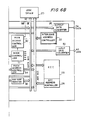
- Fig. 6 is a block diagram of the entire structure of a first embodiment of the present invention.
- Control signal (mode data) is supplied from a CPU 10 to a mode controller 12 through a CIO data bus, and an output of the mode control circuit sets a mode such as reproduction, recording and high-speed search.
- the drum In a normal reproduction mode, the drum is rotated at 2,000 rpm and digital data recorded on a magnetic tape is read out by two magnetic heads A and B.
- a synchronous clock is produced from the sync bit in the read-out data by a PLL circuit (not shown).
- the PCM data read out of a track in accordance with the synchronous clock is input to a demodulator 14.
- the demodulator 14 detects the sync signal SYNC in the input PCM data block and resets a symbol counter 16 and also subjects the input PCM data to 10 - 8 bit conversion.
- the symbol counter 16 counts the synchronous clocks and counts ID code data W1, block address data W2, parity P and PCM data, namely, 35 symbols in total (1 symbol after 10 - 8 conversion consists of 8 bits), which are input after the sync signal SYNC.
- the lower 5 bits A0 to A4 of the address counter 18 are counter outputs for counting the 32 symbols of the PCM data, while the upper two bits A12 and A13 are bits for outputting a head switching signal for the magnetic heads A and B and a 1/2 frequency division signal thereof.
- the RAM 20 having 128 KB is accessed by the output of the address counter 18 and the PCM data symbol output from the demodulator 14 is written in the RAM 20.
- the other half part 64 KB is accessed at the sampling frequency by an interleave address controller 22, and the PCM data stored at the address which is designated by the interleave address controller 22 is supplied to an output data converter 24, which converts the PCM data of 8 bits into the data of 16 bits and supplies it to a D/A converter for reproduction.
- an ECC address controller 26 accesses the RAM 20 and supplies the PCM data to an ECC circuit 28.
- the ECC circuit checks a C1 code from the input data and writes again the corrected data into the RAM 20.
- the ECC address controller 26 and the ECC circuit 28 check a C2 code so as to correct the data.
- a control signal designating the recording mode and the sampling frequency is supplied from the CPU 10 to the mode controller 12, and the internal circuit is set at the recording mode.
- Data subjected to A/D conversion in accordance with the designated sampling frequency is input to an input data converter 30, which separates the data of 16 bits into data of 8 bits.
- the symbol which is converted into 8 bits is interleaved and written into the part of 62 KB of the RAM 20 by the interleave address controller 22.
- the C1 codes and C2 codes are produced from the written symbol by the ECC circuit 28, and are stored again in a predetermined area of the RAM 20.
- the CPU 10 outputs SUB code data which is recorded together with sound data to a SUB code register 32.
- the SUB code register 32 produces pack data including a parity on the basis of the stored SUB code data.
- a pack address controller 34 writes the thus-produced pack data into the area of 64 KB for storing the C1 and C2 codes of the RAM 20 which has finished writing data into the magnetic head.
- the EEC circuit 28 produces the C1 code from the written pack data and it is stored again in the RAM 20.
- the address of the RAM 20 is first designated by a symbol counter 36, a block counter 38 and a frame counter 40 or counting written clocks FCH which are synchronous with the rotation of the rotary drum.
- the data stored in the designated address is input to a modulator 44 through a switching circuit 42 and supplied to the magnetic heads A and B after 8 - 10 bit conversion.
- a W1, W2 parity generating data register 46 stores the sub code data (W1, W2 9P) produced by the CPU 10 and supplies them to the switching circuit at a predetermined timing.
- a W1, W2 detector 48 checks the parity of the read sub code data W1, W2 on the basis of P and fetches the data having the identified parity. Among the fetched data, the data which are identified by the greatest majority are supplied to the CPU 10.
- the switching between the writing and reading into and from the RAM 20 with a change in the mode such as the reproduction mode and the recording mode are executed in accordance with the access control signal from a RAM access controller 50.
- the sub code data W1, W2 are detected with high accuracy by the W1, W2 detector while discriminating the function between FF search and REW search at the time of high-speed search.
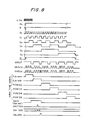
- the structure of the W1, W2 detector 48 will be explained with reference to the timing charts of Figs. 7 and 8.
- the W1, W 2 detector 48 fetches the sub code data such as W1, W2 which are read out of the magnetic tape and checks the parity of W1, W2.
- the parity is a simple parity of W1 + W2 and the checking operation can be carried out by a simple comparator or the like. An example of such a comparing circuit will be described later. If the parity is identified, the data W1 and W2 are temporarily fetched as correct data, which are subjected to judgement as to the greatest majority in the identified parities.
- a parity signal Pa which becomes [H] when a parity is identified is input to temporary storage flip-flops 60, 62 as a clock. With the rise of the parity signal Pa, the temporary storage flip-flops 60, 62 fetch and latch the data W1, W2, respectively.
- the parity signal Pa is also input to a rise detector 64.
- the rise detector is composed of two flip-flops 64a, 64b connected in series with each other and a NAND gate 64c, and the Q-output terminal of the flip-flop 64a is connected to the input terminal of the flip-flop 64b and the Q-output terminal the flip-flop 64a and the Q -output terminal of the flip-flop 64b are connected to the NAND gate 64c.
- a clock of 4.7 MHz is also input to the flip-flops 64a and 64b as a shift clock therefore.
- the reset signal R is input to a timing generator 66 and resets each of the flip-flops 66b to 66h of the timing generator 66. Consequently, the timing generator 66 starts the operation from the initial state every time a parity is identified.
- the timing generator 66 is composed of one NAND gate 66a and the seven flip-flops 66b to 66h.
- the flip-flops 66b to 66d constitute frequency dividers, the flip-flops 66e to 66g ID counters and the flip-flop 66h a check end detector.
- Each of the flip-flops 66b to 66h is set at 0 by the reset signal R at the time of the rise of the parity signal Pa.
- the output Q 6 of the flip-flop 66h which constitutes the check end detector is set at [H] by the rise of the parity signal Pa.
- the output Q 7 of the flip-flop 66h and a clock signal of 4.7 MHz are input to the NAND gate 66a.
- the NAND gate 66a outputs a clock signal which is generated by simply inverting the clock signal of 4.7 MHz after the rise of the parity signal P.
- the clock signal of 4.7 MHz output from the NAND gate 66a is input as a clock of the flip-flop 66b. Since the Q -output terminals and the input terminals of the flip-flops 66b, 66c and 66d are connected with each other, output signals Q0, Q1 and Q2 which are generated by dividing the frequency of the signal of 4.7 MHz are output from the output terminals of the flip-flops 66b, 66c and 66d, respectively.
- the frequency of the signal Q 2 is divided in another stage, thereby generating a signal Q3. Since the output Q 3 is input to the flip-flops 66f, 66g as a clock, the output Q4 of the flip-flop 66f is a signal produced by dividing the frequency of the output Q3 in another stage and the output Q5 of the flip-flop 66g is a signal produced by shifting the output Q4 by another shift.
- the output Q 5 of the flip-flop 66g is input to the flip-flop 66h which constitutes the check end detector as a clock. Since the input terminal and the Q -output terminal of the flip-flop 66h are connected with each other, the output Q 6 becomes [L] with the rise of Q 5, thereby the end of the checking operation is detected.
- the timing generator 66 All the outputs of the timing generator 66 are output to a signal generator 68.
- the signal generator 68 is provided with a W2 decoder 68a to which the W2 data from the temporary storage flip-flop 62 is input.
- W2 data includes data which indicates from which area are supplied the current sub codes W1, W2 latched in the temporary storage flip-flops 60, 62.
- the W2 decoder decodes the data and outputs one of area signals (Sub 1 even, Sub 1 odd, Sub 2 even, Sub 2 odd, PCMID 0, PCMID 2, PCMID 4, PCMID 6) at a level of [H].
- the area signal is input to an identity detector 68b.
- the output from an ID decoder 68c is input to the identity detector 68b and the identity detector 68b outputs a signal EQID when the area signal from the W2 decoder agrees with the output of the ID decoder 68c.
- the ID decoder 68c decodes the outputs of the ID counters 66e to 66g and outputs area time signals with the respective phases shifted in accordance with the outputs [0] to [5] of the ID counters 66e to 66g.
- the identity detector 68b has eight AND gates and the area signals Sub 1 even, Sub 1 odd, Sub 2 even, Sub 2 odd, PCMID 0, PCMID 2, PCMID 4, PCMID 6 are input to the respective AND gates, and 6 different area time signals with the phases shifted in series which are output from the ID decoder 68c are input to 6 AND gates to which the area signals Sub 1 even and Sub 1 odd, Sub 2 even and Sub 2 odd, PCMID 0, PCMID 2, PCMID 4, PCMID 6 are input, respectively.
- the reason why the number of area time signals is six is that the positions of the sub code area 1 and the sub code area 2 on the magnetic tape are distant from each other, so that discrimination between them is unnecessary.
- the outputs of Q1, Q2 of the flip-flops 66c, 66d which constitute frequency dividers in the pulse generator 66 are input to a NOR gate 68d.
- a signal SRRST which is [L] while both the outputs Q1 and Q2 are [H] is output from the NOR gate 68d.
- the output Q 0 of the flip-flop 62b, the output Q 7 of the flip-flop 62h and the signal SRRST are input to an AND gate 68e from the pulse generator 66. From the AND gate 68e, a signal SR15CK which is produced by removing the fourth signal from the output Q0 is output until the end of the checking operation.
- the signal EQID is input to an AND gate 68g through an OR gate 68f.
- the signal SRRST is also input to the OR gate 68f.
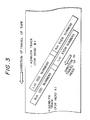
- the output Q 2 of the flip-flop 66b and the output Q of the flip-flop 68h of the pulse generator 66 are also input to the AND gate 68g. Therefore, when the signal EQID is [L], the fourth pulse is removed from the output Q0, while when the signal EQID is [H], the fourth pulse is generated. Consequently, when the signal EQID is [H], a signal SR3CK which has one more pulses than the signal SR15CK is output (Sub odd area is shown in Fig. 3).
- the W1 data is latched in the W1 temporary storage flip-flop 60 is latched when the parity is identified, as described above.
- the output terminal of the W1 temporary storage flip-flop 60 is connected to a three-stage memory 72 and a fifteen-stage memory 74 through a selecting circuit 70.
- the signal SRRST is supplied to the selecting signal as a switching signal and while the signal SRRST is [H], the output terminal of the fifteen-stage memory 74 and the input terminal of the three-stage memory 72.
- the signal SRRST is [L]
- the W1 temporary storage flip-flop 60 is connected to the input terminal of the three-stage memory 72.
- the signal SR3CK is input to the three-stage memory 72 as a shift clock, and the signal SR15CK is input to the fifteen-stage memory 74 as a shift clock. Therefore, when both of the signals SR3CK and SR15CK output three pulses, the outputs of the fifteen-stage memory 74 are serially input to the three-stage memory 72, whereby every group of three items of stored data is shifted and circulated in series.
- the signal SRRST is [L] while this pulse is output, so that the data stored in the W1 temporary storage flip-flop 60 is fetched in the three-stage memory 72.
- the fifteen-stage memory 74 does not fetch the data, so that the data stored in the third stage of the three-stage memory 72 is discarded.
- the three-stage memory 72 fetches the W1 data only when the signal EQID is [H].
- the timing for fetching the W1 data is regulated by the signal EQID, and the timing for the signal EQID in turn is regulated by the area signal.
- W1 data from each area is constantly fetched to the three-stage memory 72 at the same timing. If it is assumed that not less than three items of data are input from each area, three items of W1 data from each area are arranged in the order of Sub even, Sub odd, PCMID 0, PCMID 2, PCMID 4 and PCMID 6 in the three-stage memory 72 and the fifteen-stage memory 74. If not less than four signals for the same area are input, the old data is discarded.
- the W1 data is 8-bit data
- the output of the W1 temporary storage flip-flop 60 is 8 bits
- 9 bits are allotted to the selecting circuit 70 and 10 bits to each of the three-stage memory 72 and the fifteen-stage memory 74.
- the output of the fourth bit (bit 3) of the W2 temporary storage flip-flop 62 which indicates the discrimination between Sub 1 and Sub 2, and one of the outputs of the fifteen-stage memory 74 is selected. If the three-stage memory 72 stored new data, the output value of an AND gate 80 is written into the lowest second bit thereof.
- the output of the fifteen-stage memory 74 and a signal obtained by inverting the signal SRRST are connected to the lowest bits of the three-stage memory 72 and the fifteen-stage memory 74 through an OR gate 82. Therefore, when data is fetched to the three-stage memory 72, the lowest bit becomes [1] and in the other cases, the lowest bit becomes [0].
- the output of the fifteen-stage memory 74 is input to a comparator 84.
- the comparator 84 is composed of nine EX-OR gates 84a to 84i, one AND gate 84j, four inverters 84k to 84n, five NAND gates 84p to 84t and one AND gated 84o.
- the output of the fifteen-stage memory 74 is input to the EX-OR gates 84a to 84i and the AND gate 84j.
- the output (W1 data) of the flip-flop 60 which corresponds to the output of the fifteen-stage memory 74 are input to eight EX-OR gates 84a to 84h. If two items of data are the same, [L] is output.
- the output of the AND gate 80 is input to the EX-OR gate 84i to which the lowest second bit of the fifteen-stage memory 74 is input, and when the current output of the AND gate and the output of the fifteen-stage memory 74 agree with each other, [H] is output.
- the output terminals of the EX OR gates 84a to 84d are connected to the AND gate 84o through the inverters 84k to 84n. Therefore, when the data input to the EX-OR gates agree with each other, [H] is output to the AND gate 84o.
- the EX-OR gates 84e to 84i are connected to the AND gate 84o through the NAND gates 84p to 84s, and a search signal SE is input to the input terminals of the NOR gates 84p to 84s.
- Each of the NAND gates 84p to 84s outputs [H] of the input signal agrees with the output signal of any of the EX-OR gates 84e to 84h when the search signal SE is [H].
- the search signal SE is [L]
- each of the NOR gates 84p to 84s outputs [H] irrespective of the outputs of the EX-OR gates 84e to 84h.
- the output of the EX-OR gate 84i is connected to the AND gate 84o through the NAND gate 84t.
- the data of seventh bit the W2 data is input to the other input terminal of the NAND gate 84t.
- the NAND gate 84t outputs [H].
- the data of bit 7 of the W2 data is a signal which becomes [0] when the data is PCM data and [1] when the data is sub code data.
- the NAND gate 84t outputs [H].
- the signal SE is [L]. Therefore, the data for 4 bits (bit 0 to 3) of the W1 data is not compared. This is because the four bits of 0 to third bits of the W1 data is a signal within the frame and since the tracks are not traced during high-speed search, the data in different frames must be compared.
- the output of the AND gate 80 is input to the EX-OR gate 84i.
- the data of the fourth bit (bit 3) of the W2 data and a signal J are also input to the AND gate 80.
- the signal J becomes [L] during FF search and [H] in the other cases (e.g., REW search).
- the data of the fourth bit (bit 3) of the W2 data is a signal indicating the discrimination between the sub area 1 and the sub area 2.
- the output of the fifteen-stage memory 74 and the signal EQID are input to the NAND gate 84j. Therefore, [H] is output from the AND gate 84j only when the signal EQID is [H] and the output of the fifteen-stage memory 74 is [H]. In other words, only when the data output from the fifteen-stage memory 74 belong to the same area as the data which is fetched in the WI temporary storage flip-flop 60, the AND gate 84j outputs [H].
- the comparator 84 compares three items of W1 data output from the fifteen-stage memory 74.
- the AND gate 84o If all the inputs of the AND gate 84o are [H] as a result of comparison, the AND gate 84o outputs the pulse of [H].
- the output CNCTRCK of the AND gate 84o which shows the result of the comparison is input to a CN counter 92 through a NAND gate 90.
- the CN counter 92 for serially counting up the outputs CNCTRCK is composed of three flip-flops 92a to 92c and outputs CN1 to CN3. Each of the flip-flops 92a to 92c is risen and reset by the reset signal R from the rise detector 64 in the same way as each of the flip-flops 66b to 66h of the pulse generator 66.
- the CN counter 92 is reset and the initial value thereof is set at [001].
- each of the outputs CN1 to CN3 becomes [2], and when three pulses are input, each of them becomes [4].
- the outputs CN1 to CN3 of the CN counter 92 are input to a comparator 94 and compared with the count values LCN1 to LCN3 which are supplied from a sub code latch circuit 96.
- the sub code latch circuit 96 is provided with a pluarlity of latches for holding the W1 data and the count value from the CN counter 92 for each area.
- the W1 data, the W2 data of 3 bits and the count value are held in the sub code latch circuit 96 in accordance with the output signal, as will be described later.
- the count value is read out from each area and supplied to the comparator 94.
- the comparator 94 outputs [H] when the output of the CN counter 92 is larger than the data from the sub code latch circuit 96, and the signal [H] is input to an AND gate 98. To the AND gate 98 are also input the signals EQID and SRRST in the inverted state and the check end signal. Consequently, during the checking period, when the output of the comparator 94 is [H] and the signal EQID is [H], a signal CNLARG which is [H] while the signal SRRST is [L] is output.
- the signal CNLARG is a signal for fetching the data from the sub code latch circuit 96.
- the data of the upper 8 bits (bits 0 to 7) of the W1 temporary storage flip-flop 60, the data of 3 bits (bits 4 to 6) of the W2 temporary storage flip-flop 62 and the data of 3 bits output from the CN counter 92 are input to the sub code latch circuit 96. Therefore, the data on the number of times the W1 data has been input is stored in the sub code latch circuit 96.
- the sub code such as W1 and W2 is detected for each item of data read out by one magnetic head, namely, each item of data read out of one track.
- the head switching signal is output, the three-stage memory 72, the fifteen-stage memory 74, the sub code latch circuit 96 and the like are set at the initial stage [0].
- the checking operation is initiated.
- the W1 data and W2 data are latched in the temporary storage flip-flops 62 and 64, respectively. If the latched data are output from the Sub odd area, the signal EQID is [H] while the area time signal is Sub odd (second time) and a fourth pulse is output as the signal SR3CK, whereby the W1 data latched in the W1 temporary storage flip-flop 62 is fetched to the three-stage memory 72.
- the comparator 94 outputs [H], and sub codes W1, W2 and the count value [1] are stored in the sub code latch circuit 96.
- the sub codes W1, W2 are fetched and compared in the same way. If the sub codes are output from the same area (Sub odd area), the signal EQID becomes H at the same timing, and after three cycles of comparisons of the data by the comparator 4, they are fetched to the three-stage memory 72. In this process, the data stored in the fifteen-stage memory 74 in the previous process is output and compared with the current W1 data. If the data agree with each other, a pulse is output as the signal CNCTRCK, as shown in Fig. 3. The count value of the CN counter 92 increases to [2]. The pulse CNLARG is output from the comparator 94, whereby the W1 data and W2 data are fetched together with the value [2] of the CN counter 92 to the sub code latch circuit 96.
- the W1 data with the identified parities are stored in the corresponding areas and compared in the respective areas.
- the sub code data on the data which are identified by the greatest majority is stored in the sub code latch circuit 96.
- the necessity of judgment as to whether the data are supplied from the sub area 1 or the sub area 2 before comparison is determined.
- the data are compared without such discrimination, while at the time of REW search, they are compared after the discrimination.
- the detection of sub code with high accuracy is achieved.
- the code data is selected after judgement is made as to whether it is supplied from the sub area 1 or the sub area 2 at the time of REW search, but such discrimination is unnecessary at the time of FF search.
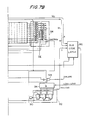
- Fig. 9 is a circuit diagram of the W1, W2 detector 48.
- the ID code data W1 of 8 bits, the block address data W2 of 8 bits, the parity P of 8 bits are held by a W1 register 48a, W2 register 48b and a P register 48c, respectively.
- each of the registers is composed of a D-type flip-flop DFF and a count-up signal is input every 8 bits from a binary counter 14a to the clock terminal of the D-type flip-flop DFF, whereby the W1 data, the W2 data and the parity P are serially input to the subsequent registers.
- the W1 data is held by the W1 register 48a in the final stage
- the W2 date is held by the W2 register 48b in the center stage
- the P data is held by the P register 48c in the first stage.
- the PCM data is stored in the address of the RAM 20 designated by the address counter 18, as described above.
- the parity calculator 48d is composed of 8 EX-OR gates, and the W1 data and W2 data each for 1 bit are input to the input terminal of each EX-OR gate.
- the EX-OR gate is a logic gate which outputs [0] when all the inputs are equal and [1] when they are different, as is well known.
- the parity P' calculated from the W1 data and W2 data in this way is output to a parity judging circuit 48e.
- the parity of 8 bits which is held by the P register 48c is also output to the parity judging circuit 48e.
- the parity judging circuit 48e judges whether or not the parity P' calculated by the parity calculator 48d is identified with the parity P.
- the parity judging circuit 48e is composed of 8 EX-OR gates each having an inversion output and an AND gate. The parities P and P' are input to the two input terminals of each EX-OR gate.
- the parity judging circuit 48e therefore outputs [11111111] when the parities P and P' are identified with each other and a value other than this when they are different.
- the data of 8 bits are output through the AND gate, so that [1] is output when P is P' and [0] is output in the other cases.
- the output from the parity judging circuit 48e, namely, the parity identity signal is input to a parity counter 48f after the rising edge thereof is detected.
- the parity counter 48f for counting the number of identified parities is composed of an 8-bit binary counter consisting of eight T-type flip-flops TFT and counts outputs [1], namely, H-level signals which are input after it is reset by both rising edge and falling edges of the head switching signal (e.g., a signal having a duty ratio of 50% which falls to an L level while the head A is reading and rises to an H Level while the head B is reading) of the upper two bits A12 and A13 of the address counter 18. Therefore, the parity counter 48f counts the number of parities which are identified by the parity judging circuit 48e for each of the magnetic heads A and B. The result of counting is output to a comparator 48g and a parity register 48h.
- the parity register 48h Since a latch signal is input to the clock terminal of the parity register 48h at the rising edge of the head switching signal, namely, when the head A is switched over to the head B, the parity register 48h outputs the number of identified parities of the data read out by the magnetic head A to the comparator 48g. In this way, the number of identified parities of the data read out by the magnetic head A and the number of identified parities of the data read out by the magnetic head B are alternately input to the comparator 48g for every one frame (corresponding to two tracks).
- the comparator 48g compares the numbers and if A > B, namely, if the number of identified parities of the data read out by the magnetic head A is larger than the number of identified parities of the data read out by the magnetic head B, [L] is output to a controller 51, while if B > A, namely, the number of identified parities of the data read out by the magnetic head B is larger than the number of identified parities of the data read out by the magnetic head A, [H] is output to a controller 51.
- the controller 51 is composed of an EX-OR gate 51a for inputting the output of the comparator 48g, an AND gate 51b for inputting the output of the EX-OR gate 51a and an OR gate 51c for inputting the output of the AND gate 51b. To the other input terminal of the EX-OR gate 51a is input the head switching signal.
- the EX-OR gate 51a outputs [H] when the comparator 48g outputs [L] because the result of comparison is A > B and when the magnetic head B is selected.
- the comparator 48g outputs [H] because the result of comparison is B > A and when the magnetic head A is selected
- the EX-OR gate 51a also outputs [H]. In other words, with respect to the data which have a small number of identified parities and are not used as reproduced data, [H] is output one frame behind in correspondence with the current head switching signal.
- the output of the EX-OR gate 51a is input to the AND gate 51b. Since a cue/review mode signal is input from the mode controller 12 to the other input terminal of the AND gate 51b, the EX-OR gate 51a outputs [H] when the mode is [H] indicating the cue/review mode and the output of the EX-OR gate 51a is [H].
- the output of the AND gate 51b is input to the OR gate 51c and output to the output data converter 24 as an error flag signal.
- the PCM data for one frame is stored in the half part of the RAM 20, namely, 64 KB and simultaneously the PCM data for the previous one frame which is stored in the other half part of 64 KB is read out by the interleave controller 22 and input to the output data converter 24, as described above.
- an error flag is forcibly set on the data read out by the magnetic head A or B and judged to be an error on the basis of an error flag signal output from the controller 51.
- the output data converter 24 adopts only the correct data without any error flag set thereon and interpolates the data by an average value before reproduction.
- the data adopted at this time is data read out by either of the magnetic heads A and B, but since the PCM data is recorded in the interleave format, it is possible to reproduce the original signal.
- the magnetic head to be adopted is selected on the basis of the parity check and a cue/review function is enabled in a simple structure without the need for an external circuit such as an envelope circuit.
Landscapes
- Engineering & Computer Science (AREA)
- Signal Processing (AREA)
- Multimedia (AREA)
- Signal Processing For Digital Recording And Reproducing (AREA)
Applications Claiming Priority (4)
| Application Number | Priority Date | Filing Date | Title |
|---|---|---|---|
| JP79636/90 | 1990-03-27 | ||
| JP7963690A JPH03278377A (ja) | 1990-03-27 | 1990-03-27 | キュー/レビュー機能付きデジタルオーディオテープレコーダ |
| JP2114035A JPH0411378A (ja) | 1990-04-27 | 1990-04-27 | デジタルオーディオテープレコーダの高速サーチ回路 |
| JP114035/90 | 1990-04-27 |
Publications (2)
| Publication Number | Publication Date |
|---|---|
| EP0449214A2 true EP0449214A2 (fr) | 1991-10-02 |
| EP0449214A3 EP0449214A3 (en) | 1992-12-09 |
Family
ID=26420649
Family Applications (1)
| Application Number | Title | Priority Date | Filing Date |
|---|---|---|---|
| EP19910104782 Withdrawn EP0449214A3 (en) | 1990-03-27 | 1991-03-26 | Digital audio tape recorder |
Country Status (3)
| Country | Link |
|---|---|
| US (1) | US5235475A (fr) |
| EP (1) | EP0449214A3 (fr) |
| KR (1) | KR910017365A (fr) |
Cited By (1)
| Publication number | Priority date | Publication date | Assignee | Title |
|---|---|---|---|---|
| EP0600224A1 (fr) * | 1992-10-30 | 1994-06-08 | Sony Corporation | Appareil d'enregistrement et de reproduction magnétique |
Families Citing this family (4)
| Publication number | Priority date | Publication date | Assignee | Title |
|---|---|---|---|---|
| US5396371A (en) * | 1993-12-21 | 1995-03-07 | Dictaphone Corporation | Endless loop voice data storage and retrievable apparatus and method thereof |
| JP3466733B2 (ja) * | 1994-10-14 | 2003-11-17 | キヤノン株式会社 | 再生装置 |
| US6014278A (en) * | 1995-03-07 | 2000-01-11 | Matsushita Electric Industrial Co., Ltd. | System for recording and reproducing data having scheme for minimizing variation in record track width when recording at different data rates |
| WO2007087312A2 (fr) * | 2006-01-23 | 2007-08-02 | Population Genetics Technologies Ltd. | Décompte moléculaire |
Family Cites Families (8)
| Publication number | Priority date | Publication date | Assignee | Title |
|---|---|---|---|---|
| JP2550949B2 (ja) * | 1986-06-28 | 1996-11-06 | ソニー株式会社 | 制御信号の検出方法 |
| JPS6390075A (ja) * | 1986-10-02 | 1988-04-20 | Victor Co Of Japan Ltd | デイジタル信号復調装置 |
| JPH0535491Y2 (fr) * | 1987-04-20 | 1993-09-08 | ||
| JP2526914B2 (ja) * | 1987-07-16 | 1996-08-21 | ヤマハ株式会社 | 磁気記録再生装置の高速サ−チ装置 |
| US4876616A (en) * | 1987-07-22 | 1989-10-24 | Sony Corporation | Apparatus for reproducing a digital signal |
| US4943964A (en) * | 1987-08-12 | 1990-07-24 | Hitachi, Ltd. | PCM signal reproducing device |
| JPH01144256A (ja) * | 1987-11-30 | 1989-06-06 | Matsushita Electric Ind Co Ltd | 磁気テープ再生装置 |
| GB8800352D0 (en) * | 1988-01-08 | 1988-02-10 | Hewlett Packard Ltd | Search method for recording medium |
-
1991
- 1991-03-25 KR KR1019910004687A patent/KR910017365A/ko not_active Withdrawn
- 1991-03-26 EP EP19910104782 patent/EP0449214A3/en not_active Withdrawn
- 1991-03-27 US US07/675,841 patent/US5235475A/en not_active Expired - Fee Related
Cited By (1)
| Publication number | Priority date | Publication date | Assignee | Title |
|---|---|---|---|---|
| EP0600224A1 (fr) * | 1992-10-30 | 1994-06-08 | Sony Corporation | Appareil d'enregistrement et de reproduction magnétique |
Also Published As
| Publication number | Publication date |
|---|---|
| KR910017365A (ko) | 1991-11-05 |
| EP0449214A3 (en) | 1992-12-09 |
| US5235475A (en) | 1993-08-10 |
Similar Documents
| Publication | Publication Date | Title |
|---|---|---|
| US4604657A (en) | Apparatus for processing PCM signal | |
| EP0235782A2 (fr) | Appareil de reproduction de signaux digitaux | |
| CA1076259A (fr) | Systeme de decodage numerique insensible a la vitesse | |
| US4862297A (en) | Apparatus for reproducing a digital signal without employing tracking signals | |
| US5235475A (en) | Digital audio tape recorder | |
| KR0138119B1 (ko) | 디지털 신호 재생장치 | |
| KR910008396B1 (ko) | 메모리 제어장치 | |
| CA1174365A (fr) | Circuit de traitement de signaux mic | |
| US5124851A (en) | Data recording apparatus with recorded data verifying means | |
| JP2695186B2 (ja) | 回転ドラムヘッド磁気テープ再生装置 | |
| US4916560A (en) | Recording speed detecting apparatus | |
| US5276561A (en) | Apparatus for reproducing digital signal | |
| US5222001A (en) | Signal processing circuit of digital audio tape recorder | |
| JP3428358B2 (ja) | タイムコード信号読み取り装置 | |
| JP2523551B2 (ja) | 磁気テ−プ信号のデユ−テイ判別装置 | |
| JP2645468B2 (ja) | ディジタル信号再生装置 | |
| JP2606202B2 (ja) | 再生装置 | |
| JP2785346B2 (ja) | 再生装置 | |
| EP0410897B1 (fr) | Appareil pour reproduire des signaux numériques | |
| JPH05298606A (ja) | 回転ヘッド形ディジタル信号再生装置 | |
| JP3101528B2 (ja) | 記録再生装置 | |
| JP3444658B2 (ja) | 最尤復号器 | |
| JPH0718060Y2 (ja) | 磁気記録再生装置 | |
| JPH064403Y2 (ja) | 読取中信号発生装置 | |
| JPH0481833B2 (fr) |
Legal Events
| Date | Code | Title | Description |
|---|---|---|---|
| PUAI | Public reference made under article 153(3) epc to a published international application that has entered the european phase |
Free format text: ORIGINAL CODE: 0009012 |
|
| AK | Designated contracting states |
Kind code of ref document: A2 Designated state(s): DE FR GB NL |
|
| PUAL | Search report despatched |
Free format text: ORIGINAL CODE: 0009013 |
|
| AK | Designated contracting states |
Kind code of ref document: A3 Designated state(s): DE FR GB NL |
|
| 17P | Request for examination filed |
Effective date: 19930510 |
|
| STAA | Information on the status of an ep patent application or granted ep patent |
Free format text: STATUS: THE APPLICATION HAS BEEN WITHDRAWN |
|
| 18W | Application withdrawn |
Withdrawal date: 19931008 |