EP0450839A2 - Machine de simulation logique - Google Patents
Machine de simulation logique Download PDFInfo
- Publication number
- EP0450839A2 EP0450839A2 EP91302635A EP91302635A EP0450839A2 EP 0450839 A2 EP0450839 A2 EP 0450839A2 EP 91302635 A EP91302635 A EP 91302635A EP 91302635 A EP91302635 A EP 91302635A EP 0450839 A2 EP0450839 A2 EP 0450839A2
- Authority
- EP
- European Patent Office
- Prior art keywords
- simulation
- processors
- logic
- current state
- machine
- Prior art date
- Legal status (The legal status is an assumption and is not a legal conclusion. Google has not performed a legal analysis and makes no representation as to the accuracy of the status listed.)
- Withdrawn
Links
Images



Classifications
-
- G—PHYSICS
- G06—COMPUTING OR CALCULATING; COUNTING
- G06F—ELECTRIC DIGITAL DATA PROCESSING
- G06F11/00—Error detection; Error correction; Monitoring
- G06F11/22—Detection or location of defective computer hardware by testing during standby operation or during idle time, e.g. start-up testing
- G06F11/26—Functional testing
- G06F11/261—Functional testing by simulating additional hardware, e.g. fault simulation
-
- G—PHYSICS
- G06—COMPUTING OR CALCULATING; COUNTING
- G06F—ELECTRIC DIGITAL DATA PROCESSING
- G06F11/00—Error detection; Error correction; Monitoring
- G06F11/30—Monitoring
- G06F11/34—Recording or statistical evaluation of computer activity, e.g. of down time, of input/output operation ; Recording or statistical evaluation of user activity, e.g. usability assessment
- G06F11/3457—Performance evaluation by simulation
-
- G—PHYSICS
- G06—COMPUTING OR CALCULATING; COUNTING
- G06F—ELECTRIC DIGITAL DATA PROCESSING
- G06F11/00—Error detection; Error correction; Monitoring
- G06F11/30—Monitoring
- G06F11/34—Recording or statistical evaluation of computer activity, e.g. of down time, of input/output operation ; Recording or statistical evaluation of user activity, e.g. usability assessment
- G06F11/3466—Performance evaluation by tracing or monitoring
-
- G—PHYSICS
- G06—COMPUTING OR CALCULATING; COUNTING
- G06F—ELECTRIC DIGITAL DATA PROCESSING
- G06F30/00—Computer-aided design [CAD]
- G06F30/30—Circuit design
- G06F30/32—Circuit design at the digital level
- G06F30/33—Design verification, e.g. functional simulation or model checking
-
- G—PHYSICS
- G06—COMPUTING OR CALCULATING; COUNTING
- G06F—ELECTRIC DIGITAL DATA PROCESSING
- G06F11/00—Error detection; Error correction; Monitoring
- G06F11/30—Monitoring
- G06F11/34—Recording or statistical evaluation of computer activity, e.g. of down time, of input/output operation ; Recording or statistical evaluation of user activity, e.g. usability assessment
- G06F11/3466—Performance evaluation by tracing or monitoring
- G06F11/348—Circuit details, i.e. tracer hardware
-
- G—PHYSICS
- G06—COMPUTING OR CALCULATING; COUNTING
- G06F—ELECTRIC DIGITAL DATA PROCESSING
- G06F11/00—Error detection; Error correction; Monitoring
- G06F11/30—Monitoring
- G06F11/34—Recording or statistical evaluation of computer activity, e.g. of down time, of input/output operation ; Recording or statistical evaluation of user activity, e.g. usability assessment
- G06F11/3466—Performance evaluation by tracing or monitoring
- G06F11/349—Performance evaluation by tracing or monitoring for interfaces, buses
Definitions
- the present invention relates generally to a logic simulation machine for the simulation of digital logic, and in particular, to the recording of events occuring during simulation in such a machine. Such recording is performed by a device described as an event trace gatherer.
- Logic technologies such as very large scale integrated circuits provide significant improvements in cost/performance and reliability.
- they have disadvantages in that their fault diagnosis is more difficult than previous technologies and the engineering rework cycles needed to correct faults in logic design are greatly lengthened.
- These disadvantages exact great economic penalties for design errors and omissions and place a great emphasis on the goal of completely verifying designs in advance of engineering models.
- One technique for providing design verification is logic simulation by a general purpose computer.
- Another technique is to use a special purpose computer that is optimized for logic simulation.
- the special purpose computer usually uses a multiple processor architecture by which a number of processors, called simulation processors, may be interconnected to improve simulation performance.
- the special purpose computer may operate in combination with a host computer which is used to provide loading functions and to analyze the results of the simulation.
- a logic simulation machine Such a special purpose computer is called a logic simulation machine.
- This machine comprises a plurality of parallel basic processors which are interconnected through an inter-processor switch.
- the inter-processor switch provides communication not only among the basic processors which are computing engines of the logic simulation machine, each simulating the individual gates of a portion of a logic model in parallel, but also between them and a control processor which provides overall control and input/output facilities of the logic simulation machine through a host computer to which the control processor is attached.
- Each basic processor contains the current state information for only the set of gates that is being simulated by that processor. When a basic processor simulates a gate whose input includes a connection to the output of a gate being simulated by a different processor, the state information for the gate in question is transferred over the inter-processor switch.
- data is normally collected by having the host evaluate all of the nodes to be traced at the end of each simulation cycle.
- a logic simulation machine comprising a simulation processor operable to simulate digital logic, characterised by a trace gatherer comprising a current state store for storing current states of a model being simuluated, a change record store for storing changes in the current states of the model and a control means for monitoring the current states of the model being simulated to detect a change in the current states stored in the current state store and store the change into the change record store.
- a method of operating a logic simulation machine including a current state store means and a change record means, comprising the steps of: storing current states of a model being simulated by the logic simulation machine in the current state store means; monitoring the current states of the model being simulated to detect a change in the current states stored in the current state store means; and storing the change into the change record means.
- a common simulation bus received a simuluated result in parallel from the processors at the end of each simulation cycle in order to monitor the simulation.
- a memory unit equal in size to the current state array is preferably provided for tracing any subset of all facilities.
- the memory unit is used as a mask to store a bit for indicating the node to be traced.
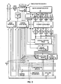
- Fig. 1 is an entire schematic block diagram of a logic simulation machine to which an AET gatherer according to a preferred embodiment of the present invention is attached.
- Fig. 2 is a schematic block diagram of the simulation processor plugged into the slot 0 in Fig. 1.
- Fig. 3 is a schematic diagram showing contents of a block description array of the simulation processor of Fig. 2.
- Fig. 4 is a schematic diagram showing the op-code field of instructions stored in the block description array of Fig. 3.
- Fig. 5 is a schematic block diagram of a simplified logic circuit model used in explaining a block description instruction and operation of the simulation processor shown in Fig. 2.
- Fig. 6 is a schematic block diagram of a current state array of the simulation processor of Fig. 2.
- Fig. 7 is a detailed schematic block diagram of a part of the simulation processor of Fig.2.
- Fig. 8 is a schematic block diagram of an outputting means of the simulation processor of Fig. 2 for putting a result from the logic function table on allocated data lines of the simulation bus.
- Fig. 9 is a simplified illustration of the block description arrays of the simulation processors in the machine of Fig. 1 to explain operation of the machine.
- Fig. 10 is a simplified illustration of the block description arrays of another configuration of the logic simulation machine.
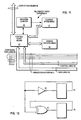
- Fig. 11 is a schematic block diagram of an all events trace (AET) gatherer according to a preferred embodiment of the invention, which is connected by the simulation bus means in parallel with the simulation processors to the logic simulation machine to generate an all events trace (AET) during a simulation.
- AET all events trace
- Fig. 12 is a schematic diagram of a 2-bit counter to be simulated by the machine of Fig. 1 to explain operation of the all events trace (AET) gatherer of Fig. 11.
- AET all events trace
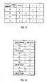
- Fig. 13 is a table to explain the current states of nodes in the counter of Fig. 12 at each simulation cycle.
- Fig. 14 is a table showing contents of a change record array to explain the operation of the all events trace (AET) gatherer of Fig. 11.
- AET all events trace
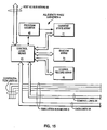
- Fig. 15 is a block diagram showing an all events trace (AET) gatherer according to a second embodiment of the invention.
- the logic simulation machine 1 which is the subject of the co-pending application US Serial No. filed and having internal docket No. AT9-89-099 includes plural simulation processors 2 connected to each other in parallel through a simulation bus means 3. Although four simulation processors 2 are shown in Fig. 1, the number of the simulation processors 2 connected to the simulation bus means 3 is sixteen and sixteen processors are a maximum configuration for explanation purpose. However, any number of simulation processors selected from a group consisting of 1, 2, 4, 8, and 16 is able to be used in the machine 1.
- the simulation bus means 3 comprises three parts: data lines 3A through which each simulation processor 2 transfers a simulated result and each simulation processor 2 receives the results from all simulation processors 2 to update its own copy of current states when evaluating gates and through which a host computer 5 transfers packet data to and from the simulation processors 2 when not evaluating gates; control lines 3B through which current contents on the data lines 3A are indicated and arbitration for the bus 3 is done; and configuration lines 3C through which a unique code is transferred to each of the simulation processors 2 to inform the configuration of the simulation processors.
- the simulation bus means 3 further comprises slot means 0, 1, 2,..., 15 and n. Each simulation processor 2 is plugged into the slot means 0, 1, 2,..., or 15 for connection with the simulation bus means 3.
- Each slot means 0, 1, 2,..., or 15 of the simulation bus means 3 has a hard wired means 3D associated with the configuration lines 3C.
- the number of the configuration lines 3C depends on how many simulation processors 2 the logic simulation machine 1 can contain. In this embodiment, the number of the lines 3C is four to convey a different 4-bit binary data to each of the sixteen simulation processors.
- the hard wired means 3D of the slot means 0 sets all lines of the configuration lines 3C OFF so that the configuration lines 3C input 4-bit binary zero data 0000 into the simulation processor 2 plugged into the slot means 0.
- the hard wired means 3D of the slot means 1 sets the least significant bit line ON and the other three lines OFF so that the configuration lines 3C input binary data 0001 into the simulation processor 2 plugged into that slot means.
- the hard wired means 3D of the slot means 2 sets the second least significant bit line ON and the other three lines OFF so that the configuration lines 3C input binary data 0010 into the simulation processor 2 plugged into that slot means and so on.
- the hard wired means 3D of the slot means 15 sets all lines ON so that the configuration lines 3C input binary data 1111 into the simulation processor 2 plugged into that slot means.
- An all events trace (AET) gatherer 4 of the invention which is an auxiliary processor in the machine 1 is plugged into the slot means n of the bus means 3 for connection with the simulation bus means 3 in parallel with the simulation processors 2.
- the number of the data lines 3A depends on how many simulation processors 2 the logic simulation machine 1 can contain and how many bits each simulation processor 2 needs to represent a calculated result.
- Each of the simulation processors 2 is allocated two data lines 3A to transfer a result calculated by that processor to all of the simulation processors 2, depending upon which slot means that processor 2 occupies as explained later.
- the data lines 3A can also be used by the host computer 5 to load data and instructions into each of the simulation processors 2 and the AET gatherer 4 before simulation and to receive the results calculated by the simulation processors 2 and the AET gatherer 4 during the simulation through a host interface provided in one of the simulation processors 2 as explained later.
- the host computer 5 may be a conventional engineering workstation.
- the host computer 5 includes a central processing unit 51, a main memory 52, a disk file (direct access storage device) 53, a keyboard 54, a display 55, and a host I/O bus means 56.
- Each of the simulation processors 2 and the AET gatherer 4 are connected to the host computer 5 through the I/O bus means 56 by being plugged into slot means (not shown) of the I/O bus means 56. If the number of the simulation processors 2 exceeds the number of the I/O slot means provided within the host computer 5, an extension housing may be used to connect the additional simulation processors to the host computer 5.
- the simulation processors 2 and the AET gatherer 4 are provided on rectangular cards. Connector (not shown) for the slot (not shown) of the host I/O bus means 56 is provided at one end of the card on which the simulation processor 2 or the AET gatherer 4 is mounted. Connector (not shown) for the slot means 0, 1, ..., 15 or n of the simulation bus means 3 is provided at the opposite end of the card.
- the simulation processors 2 and the AET gatherer 4 are installed in the host 5 by directly plugging the connector (not shown) at the one end of the card into the slot (not shown) of the host I/O bus 56.
- the simulation bus means 3 connects the simulation processors 2 and the AET gatherer 4 by plugging the slot means 0 thru n into the connectors (not shown) at the opposite end of the cards.
- Each simulation processor 2 has seven primary elements: a first memory unit, such as a block description array 22; a second memory unit, such as a current state array 23; a logical function table 24; an outputting means 25; a bus steering means 80; a program counter 26; and a control logic means 27.
- the block description array 22 is an instruction memory for the simulation processor 2 which contains all of the information necessary to specify operations of that simulation.
- Fig. 3 shows contents of the block description array 22.
- An instruction stored at one address in the array 22 contains an op-code field (16 bits), A1, A2, A3, and A4 fields (each 24 bits in this embodiment).
- one instruction word corresponds to each logical block or gate in a model to be simulated.
- the instruction word's address represents a block or gate identifier.
- the instruction contains the op-code field, to specify a logical function of the gate, such as AND or OR, and four fields A1, A2, A3 and A4, to specify input connections or input operands of the gate.
- a block description instruction corresponds to a single 1-output, 4-input gate.
- the logical function of the gate is determined by an 8-bit function pointer FFFFFFFF in the op-code which is an index to the logical function table 24.
- Input/output inversion can be done independent of the logical function table 24 by inversion bits I1, I2, I3, I4, and I0 in the op-code.
- the fields A1, A2, A3, and A4 represent addresses in the current state array 23 where the four input operands are stored.
- the block description instruction's address in the block description array 22 implies its output address in the current state array 23 where the calculated result is to be stored.
- the size of the block description array 22 depends on a desired capacity of the simulation processors 2. In this embodiment, the array 22 can store up to 512 K block description instructions.
- Fig. 5 shows an example of a gate to be simulated by the simulation processor 2 in order to illustrate the block description instruction shown at an address Z in Fig. 3.
- An AND gates is identified by a numeral Z which corresponds to an address in the block description array 22 where the block description instruction of the gate is stored.
- the AND function pointer and the invert functions of the gate are stored in the op-code field of the instruction.
- Input connections V, W, X, and Y of this gate are stored in the fields A1, A2, A3 and A4 of the instruction.
- the current state array 23 stores input operands of the gate Z at addresses V, W, X, and Y designated by the fields A1, A2, A3, and A4.
- the op-code field specifies a control function executed by the simulation processors.
- Halt means to stop the simulation to wait for host interaction.
- Broadcast means to send any packet of data to the simulation bus means 3 for use by the host and/or an auxiliary processor connected to the simulation bus 3.
- Branch means to go to an instruction stored in the address designated by the fields A2 and A3.
- the current state array 23 is a memory which stores a complete copy of current states of a whole model being simulated.
- the state of each block or gate is specified by 2 bits.
- the possible states are logical 0 (00), logical 1 (01), Undefined (10) and High Impedance (11).
- the current state array 23 stores such current states of all blocks or gates of the machine being simulated.
- the current state array 23 must have 1 M bit capacity at least. In this example, however, the current state array 23 is larger to achieve maximum performance.
- the contents of the current state array 23 are simultaneously addressed by the four fields A1, A2, A3 and A4. It is preferred to read the current states of four different blocks or gates simultaneously. Therefore, the array 23 is replicated 4 times. When reading the array 23, four different addresses can be read simultaneously. When writing the array 23, the same addresses in all four arrays are always written. That is, when the current state array 23 is read, the multiplexors 62 are controlled through an address selection by the control logic means 27 to output addresses A1, A2, A3, and A4 to each array. Then, each array outputs a 2-bit operand to an operand invert logic means 63.
- Each of the outputted operands may be inverted by the inversion bit of the op-code in the means 63 before calculation in the logical function table 24.
- the multiplexors 62 are controlled through the address selection by the control logic means 27 to output one address A0. Then, the same data is written into the four arrays at the same address A0.
- this could been done using a single array and time-slicing, but at the expense of roughly 4 times performance.
- another 4 arrays are added in the example shown in Fig. 6. For unit delay simulation, the state of the machine being simulated need to be saved in a "master-slave" arrangement.
- next state of the machine needs to be computed before this becomes the current state of the machine.
- the simplest way to implement this is with two memory (A and B) operating in a ping-pong arrangement.
- A contains the current state
- B will be used to save the next state.
- A is used to save the next state.
- the logical function table 24 is a programmable logic block whose main element is a memory 65, a 64K x 2bit static RAM, indexed by the 8-bit function pointer in the op-code field plus the four 2-bit input operands form the operand invert logic 63.
- the logical function table 24 generates a 2-bit output, which is the next state of the gate being evaluated.
- the RAM 65 is also accessible to the host computer 5 through a multiplexor 67, which needs to load it with a set of logical functions prior to beginning of the simulation.
- the logical function table 24 is in essence a look up table which generates a 2-bit output with respect to a given gate function and four input operands.
- the output of the logic function table 24 is supplied to the outputting means 25 through an output invert logic means 66.
- the output from the table 24 may be inverted in the output invert logic means 66 by the inversion bit of the op-code before being put on the allocated lines of the data lines 3A through the outputting means 25.
- the outputs from the operand invert logics 63 are also supplied to the bus steering means 80.
- the bus steering means 80 receives four current states designated by A1 thru A4 fields of the command from the current state array 23 through the operand invert logics 63 and puts eight bit data on the data lines 0 thru 7, 8 thru 15, 16 thru 23, or 24 thru 31 under the control of the control logic 27.
- the data in the current state array 27 are sent to the host 5 by the Broadcast command from the simulation processors 2 for use in the host 5.
- the Broadcast command is the subject of the co-pending application US Serial No. filed and having internal docket No. AT9-89-098.
- the outputting means 25 comprises 16 AND gates E0, E1,..., and E15, 16 gates L0, L1,..., and L15 whose outputs are connected to the even number lines 0, 2,..., and 30 of the data lines 3A, respectively, and 16 gates H0, H1,..., and H15 whose outputs are connected to the odd number lines 1, 3,..., and 31 of the data lines 3A, respectively.
- the configuration lines 3C which are connected to the hard wired means 3D and the control logic means 27 are connected to inputs of the AND gates E0, E1,..., and E15. All inputs from the lines 3C to the gate E0 are inverted so that only the 4-bit binary data 0000 on the lines 3C can activate the gate E0.
- An input from the least significant bit line of the lines 3C is directly connected to the gate E1 and the other three inputs from the lines 3C to the gate E1 are inverted so that only the 4-bit binary data 0001 can activate the gate E1 and so on. All inputs from the lines 3C are directly connected to the gate E15 so that only the 4-bit binary data 1111 on the lines 3C can activate the gate E15.
- a running mode signal from the control logic 27 is also connected to input of each of the AND gates E0, E1,..., and E15 to activate the AND gates during running mode of the simulation processors 2. Outputs of the AND gates E0, E1,..., and E15 are connected to enable terminals of the gates L0 and H0, L1 and H1,..., and L15 and H15, respectively.
- the low bit line of the output from the output invert logic means 66 is connected to inputs of the gates L0, L1,..., and L15.
- the high bit line of the output from the output invert logic means 66 is connected to inputs of the gates H0, H1,..., and H15.
- control logic means 27 controls a clock means 68 so that all of the simulation processors 2 connected with the simulation bus means 3 synchronously execute their operations.
- the control logic means 27 controls the program counter 26 so that the program counter 26 generates addresses to output instructions from the block description array 22 and addresses to write the calculated results from all of the simulation processors 2 back into the current state arrays 23.
- the control logic means 27 control the control instructions, such as Branch, Broadcast, and Halt.
- the control logic means 27 also controls the simulation processor 2 to load the block description array 22 with instructions and the current state array 23 with initial states from the host computer 5 before simulation.
- the simulation processor 2 occupying the slot 0 contains the host interface 21 to transfer data and instructions between the host 5 and the simulation processors 2.
- the host interface 21 is a First-In First-Out buffer to buffer data between the simulation bus means 3 and the host I/O bus means 56.
- control logic in the host interface 21 determines, by the contents of the control lines 3B, that the data on the data lines 3A is intended for the host and transfers the data to the host 5.
- the host interface means 21 allows the user to initialize the block description arrays 22 and the current state arrays 23 at the beginning of the simulation and test results at the end of the simulation. It may also allow the user to read and modify the contents of the current state arrays 23 during the simulation for enhanced simulation capability.
- the host interface is the subject of the co-pending application US Serial No. filed and having internal docket No. AT9-89-097.
- the host computer 5 is used to personalize the simulation processors 2 on power-on operation, to load the simulation processors 2 with instructions and data before the simulation, to evaluate the results during and/or after the simulation, and to interface with user.
- the host computer 5 personalizes each of the simulation processors 2 directly through the I/O bus means 56.
- the host counts the number of the simulation processors 2 plugged into the I/O slots and tells the simulation processors 2 the number.
- the host does not need to take care of the configuration of the simulation processors 2 as explained later.
- the host computer 5 communicates with the simulation processors 2 only through the host interface 21 provided in the simulation processor 2 plugged into the slot 0 of the simulation bus means 3 except power supply through the I/O slot.
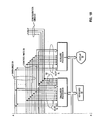
- the host computer 5 When loading the instructions into the block description array 22 of each of the simulation processors 2, the host computer 5 sends instructions to the simulation bus means 3 through the I/O bus 56 and the host interface 21. Each simulation processor 2 takes by turns the instructions and stores them into the block description array 22. Thus, as shown in Fig. 9, the simulation processors 2 plugged into the slot means 0, 1,..., and 15 store consecutively the block description instructions for gates 0, 16, 32,..., gates 1, 17, 33,..., and gates 15, 31, 47,..., in their block description arrays 22, respectively, and store the same control instructions at the same addresses in the block description arrays 22.
- the host computer 5 loads the same initial states of a whole model to be simulated by the machine 1 into the current state array 23 in each of the simulation processors 2.
- the current state array 23 in each simulation processor 2 maintains a complete copy of current states of the whole model being simulated during the simulation as explained later.
- the host computer also loads the same functional data into the logical functional table 24.
- each simulation processor 2 continuously steps through its block description array 22, evaluating each gate's next state, until it receives a command to stop that can be either imbedded in the block description array 22 or come from the host computer 5.
- the stopped mode no simulation is occurring, and the entire state of the logic simulation machine 1 including the current state array 23 and the block description array 22 is available for inspection and modification by the host computer 5.
- this logic simulation machine 1 allows the sixteen simulation processors 2 to work on one simulation model to speed up simulation.
- each simulation processor 2 evaluates one gate per cycle. At the end of the cycle each simulation processor 2 puts its result on the allocated lines of the data lines 3A in parallel and all simulation processors 2 update their current state arrays 23 with the results from the data lines 3A.
- each simulation processor 2 which is plugged into the simulation bus means 3 until a Halt command is found from the block description array 22 or the host computer 5 stops the simulation.
- the control logic means 27 sequentially increments the program counter 26 from a start address to sequentially output instructions from the block description array 22.
- the block description array 22 When the block description array 22 is addressed by the program counter 26, it outputs an instruction stored in the corresponding address.
- the op-code field of the instruction is latched by a latch 61.
- the op-code field indicates whether it is a block description instruction or a control instruction. If it is a block description instruction, the op-code field describes the function of the gate being evaluated.
- the fields A1 thru A4 specify four input connections of the gate being evaluated and correspond to addresses in the current state array 23 where the current states of the input connections are stored.
- the addresses A1 thru A4 are passed to the array 23 through the multiplexors 62.
- Four 2-bit current states that are input operands to the gate being evaluated are simultaneously fetched from the addresses designated by the fields A1 thru A4. These input operands are sent to the operand invert logic means 63 so that the operands are inverted if the op-code indicates before the calculation in the logical function table 24.
- the input operands to the gate being evaluated are sent to the logical function table 24.
- This information along with the function pointer of the op-code field describing the gate's function from the latch 61, serves as a pointer into the logical function table 24.
- the logical function table 24 is in essence a look up table, and generates a proper 2-bit output value for the gate given its present inputs.
- the output of the logical function table 24 is sent to the output invert logic 66 so that the output is inverted if the op-code indicates.
- the result from the output invert logic means 66 is supplied to the outputting means 25 to be put on the allocated lines of the data lines 3A in order to update all the current state arrays 23 in the machine 1 with the result.
- the AND gate shown in Fig. 5 is evaluated as follows:
- the program counter 26 of the simulation processor plugged into the slot 0 generates an address Z to fetch the block description instruction of the gate from the block description array 22.
- Four operands H(0,1), H(0,1), L(0,0), and L(0,0) are fetched from the addresses V, W, X, and Y in the current state array 23 as designated by the fields A1 thru A4 of the block description instruction.
- All four L(0,0) input operands and an function pointer specifying AND function are inputted to the table 24.
- the table 24 outputs a result, L(0,0). This result is inverted to H(0,1) in the output invert logic means 66 by the op-code.
- the output H(0,1) is supplied to the outputting means 25 to transfer to all the simulation processors 2 to update their current state arrays 23.
- the processors 2 in the slot 0, 1, 2,..., and 15 put their 2-bit results on the allocated lines 0 and 1, 2 and 3, 4 and 5,..., and 30 and 31 of the data lines 3A, respectively. In this way, all results calculated in this cycle appear on the data lines 3A in parallel.
- the results on the data lines 3A are received by the control logic means 27 and are written back to 16 adjacent addresses beginning at an address designated by the product of the simulation cycle number and the number of the simulation processors in the configuration (16 in this embodiment), in the current state array 23 in each of the processors 2 at the end of each simulation cycle. For example, at the end of the first simulation cycle, addresses 0 thru 15 in the current state arrays 23 of all the simulation processors are updated with results on the data lines 3A.
- addresses 16 thru 31 in the current state array 23 are updated with results on the lines 3A.
- addresses 32 thru 47 and so on are updated.
- the current state array 23 in each simulation processor 2 is updated with the results calculated at each simulation cycle by all of the processors 2 and keeps a complete copy of current states of the model being evaluated in the machine 1.
- the host computer 5 can receive the results through the data lines 3A and the host interface 21 during the simulation by the Broadcast command and/or after the simulation from the currrent state array 23 of the processor 2 plugged into the slot 0.
- the identical control instructions are executed simultaneously in all of the simulation processors 2 for proper synchronization of the simulation. For, example, Branches are resolved identically across all simulation processors 2 at a time.
- the configuration of the simulation processors 2 is kept transparent from the host computer 5 and the same model built for the largest configuration can be used irrespective of the changes in the configuration because the control logic 27 and the configuration lines 3C inform the simulation processors of the configuration to take care of the configuration change by themselves.
- the host computer 5 communicates with the logic simulation machine 1 through the host interface 21 of the processor 2 plugged into the slot 0 of the simulation bus means 3. Then, the group of the simulation processors 2 appear to the host computer 5 as a single entity with respect to a number of tasks; building the simulation model, loading it into the simulator, running the simulation, and retrieving the results for analysis.
- each simulation processor 2 receives by turns and stores the instructions in the block description arrays 22 as shown in Fig. 10.
- Each control logic means 27 in the processors 2 executes the first Branch or Halt control instruction of the four identical control instructions and neglects the other three redundant identical control instructions since the four Branch or Halt commands have the same contents. However, all Broadcast instructions are executed by the processors 2 since each of the sixteen broadcast commands contains different operands in the fields A1 thru A4 to transfer data from the array 23 to the host 5.
- the machine 1 makes the number of simulation processors transparent to software. This means that architecturally 16 block description instructions are always executed simultaneously. In fact, this may take 1, 2, 4, 8, or 16 cycles, depending on the number of the simulation processors, but the software does not see a difference.
- the host computer accesses the block description arrays in the simulation processors for loading or other purposes, it sees simply one set of instructions. Physically, the hardware of the simulation processors may direct the host's accesses to different arrays on multiple cards, but the host does not see this. If a logic model to be simulated is built for the largest configuration of the logic simulation machine the model will run on any smaller configuration without any modification. This concept allows the same model to be used across many hardware configurations. The host does not need to know the configuration but just sends all host data to the I/O bus regardless of the configuration. This is important particularly because the architecture of this example allows the user to reconfigure the logic simulation machine at any time in order to get a desired performance.
- the simulation processors 2 will normally be used to simulate only gate logic, functions such as memory or array modelling and device behavioral will be performed by the host computer 5.
- all data to and from the host computer 5 goes on the simulation bus means 3, the host becomes just another device on the bus 3.
- Obvious candidates for the hardware accelerator or the auxiliary processor is trace collection, memory or array simulation, and device behavioral, where the host may be slowing down the simulation throughput. In fact, all functions except user interface could be migrated to an auxiliary processor to relieve such a host work.
- the all events trace (AET) gatherer 4 of the invention is an example of such an auxiliary processor.
- An all events trace (AET) is a record of what has happened to all of the facilities during a simulation.
- the AET data is normally collected by having the host computer 5 evaluate all of the nodes to be traced at the end of each simulation cycle in the prior art. Even with the efficiencies of the Broadcast command to send only those nodes of interest to the host, two limitations remain. First all of the nodes to be traced are sent to the host computer, even those that did not change. Second, it places a considerable time requirement on the host to evaluate the data every simulation cycle.
- the AET gatherer 4 generates an AET data in parallel with the simulation to relieve the host task.
- the AET gatherer 4 has the same components as those of the simulation processor 2, that is, a current state array 41 that keeps a complete copy of current states of the whole model being simulated by monitoring the simulation bus means 3 and a program counter 42 which is synchronized with the simulation processor 2.
- the AET gatherer 4 has its control logic means 43 and a change record array 44 to store only changes in the model being simulated.
- the current state array 41 is constituted by one array and does not need to have four or eight identical arrays as the simulation processors 2.
- the current state array 41 is updated with calculated results on the data lines 3B at the end of each simulation cycle in the same way as the current state array 23 in the processors 2.
- the control logic 43 puts a marker in the change record array 44 to indicate the cycle begin point.
- the control logic 43 monitors the simulation bus means 3 to keep a complete copy of the current states in the current state array 41. By comparing the new values of each node address as they are generated against the old value in the current state array 41, the control logic 43 detects a change in the node. Whenever a change is detected, the control logic 43 stores the node address and new node value in the change record array 44.
- Fig. 12 shows a design model, a two-bit counter, to be simulated by the simulation processors 2 in the logic simulation machine 1.
- Fig. 13 shows the states of all the nodes in the current state array 41 at the end of each simulation cycle, all nodes in the model having been evaluated once.
- Fig. 14 shows the contents of the change record array 44 after three simulation cycles. Only changed nodes and new values are stored in the change record array 44.
- Fig. 15 shows an AET gatherer 4 according to a second embodiment of the invention to trace any subset of all facilities during the simulation.
- the AET gatherer 4 includes the same components as those in Fig. 11 in addition to the shadow array 71 which has the same size as the current state array 41 to store a bit for indicating the node to be traced so that any subset of all facilities can be traced.
- the shadow array 71 is used as a mask when the control logic 43 examines a change between the current states stored in the current state array 41 and the calculated results from the simulation bus 3 to generate the AET records for a subset of all facilities.
- the shadow array may be constituted by one of four identical arrays of the current state array 23 of the processor 2.
- the AET gatherer 4 is a passive auxiliary processor which only monitors the simulation bus means 3. The only time it affects the simulation is if it must halt simulation to dump the change record array 44 to the host. This should happen rarely if ever, and can be avoided entirely if the host has bandwidth to handle both the simulation and AET dump. Since AET gatherer 4 is recording a minimum of information (changes only), if the change record array 44 is large enough and the number of facilities to be traced is reasonable, most simulation cases can be completed before the AET dump is required.
- the AET gatherer 4 generates the AET by monitoring the simulation bus 3 without slowing down the tasks of the simulation processors and of the host computer and also allows any subset of facilities to be collected by using the shadow array storing a mask which indicates which nodes are to be traced.
- the number of the simulation processors connected to the simulation bus means is 2 n and the maximum number is sixteen.
- the AET gatherer of the invention is able to be attached to a logic simulation machine which contains any number of the simulation processors so that the AET gatherer monitors the data on the simulation bus means in order to gather an AET in parallel with the simulation.
Landscapes
- Engineering & Computer Science (AREA)
- Theoretical Computer Science (AREA)
- General Engineering & Computer Science (AREA)
- Computer Hardware Design (AREA)
- Physics & Mathematics (AREA)
- General Physics & Mathematics (AREA)
- Quality & Reliability (AREA)
- Evolutionary Computation (AREA)
- Geometry (AREA)
- Test And Diagnosis Of Digital Computers (AREA)
Applications Claiming Priority (2)
| Application Number | Priority Date | Filing Date | Title |
|---|---|---|---|
| US07/502,148 US5327361A (en) | 1990-03-30 | 1990-03-30 | Events trace gatherer for a logic simulation machine |
| US502148 | 1990-03-30 |
Publications (2)
| Publication Number | Publication Date |
|---|---|
| EP0450839A2 true EP0450839A2 (fr) | 1991-10-09 |
| EP0450839A3 EP0450839A3 (en) | 1993-02-24 |
Family
ID=23996560
Family Applications (1)
| Application Number | Title | Priority Date | Filing Date |
|---|---|---|---|
| EP19910302635 Withdrawn EP0450839A3 (en) | 1990-03-30 | 1991-03-26 | A logic simulation machine |
Country Status (3)
| Country | Link |
|---|---|
| US (1) | US5327361A (fr) |
| EP (1) | EP0450839A3 (fr) |
| JP (1) | JPH0738202B2 (fr) |
Cited By (1)
| Publication number | Priority date | Publication date | Assignee | Title |
|---|---|---|---|---|
| US5649164A (en) * | 1994-12-30 | 1997-07-15 | International Business Machines Corporation | Sets and holds in virtual time logic simulation for parallel processors |
Families Citing this family (43)
| Publication number | Priority date | Publication date | Assignee | Title |
|---|---|---|---|---|
| US8050903B1 (en) * | 1990-05-29 | 2011-11-01 | Texas Instruments Incorporated | Apparatus and method for checkpointing simulation data in a simulator |
| WO1992000654A1 (fr) * | 1990-06-25 | 1992-01-09 | Barstow David R | Procede de codage et de diffusion d'informations relatives a des evenements en direct utilisant des techniques informatiques de simulation et de concordance avec un modele |
| US7373587B1 (en) | 1990-06-25 | 2008-05-13 | Barstow David R | Representing sub-events with physical exertion actions |
| EP0508619A2 (fr) * | 1991-04-11 | 1992-10-14 | Hewlett-Packard Company | Interface de stimuli à socle bidirectionnel pour un simulateur logique |
| JPH0546697A (ja) * | 1991-08-14 | 1993-02-26 | Nec Corp | 論理シミユレータ |
| JP3119960B2 (ja) * | 1993-03-17 | 2000-12-25 | 富士通株式会社 | 論理シミュレーションシステム |
| US5828867A (en) * | 1994-08-04 | 1998-10-27 | Lucent Technologies Inc. | Method for discrete digital event simulation |
| US5678028A (en) * | 1994-10-25 | 1997-10-14 | Mitsubishi Electric Information Technology Center America, Inc. | Hardware-software debugger using simulation speed enhancing techniques including skipping unnecessary bus cycles, avoiding instruction fetch simulation, eliminating the need for explicit clock pulse generation and caching results of instruction decoding |
| US5737578A (en) * | 1994-11-18 | 1998-04-07 | International Business Machines Corp. | Apparatus and method for partitioning multiport rams |
| US5546562A (en) * | 1995-02-28 | 1996-08-13 | Patel; Chandresh | Method and apparatus to emulate VLSI circuits within a logic simulator |
| US5774380A (en) * | 1996-03-08 | 1998-06-30 | International Business Machines Corporation | State capture/reuse for verilog simulation of high gate count ASIC |
| US5907695A (en) * | 1996-03-22 | 1999-05-25 | Sun Microsystems, Inc. | Deadlock avoidance mechanism for virtual bus distributed hardware simulation |
| US5881267A (en) * | 1996-03-22 | 1999-03-09 | Sun Microsystems, Inc. | Virtual bus for distributed hardware simulation |
| US5878208A (en) * | 1996-11-25 | 1999-03-02 | International Business Machines Corporation | Method and system for instruction trace reconstruction utilizing limited output pins and bus monitoring |
| US5911059A (en) * | 1996-12-18 | 1999-06-08 | Applied Microsystems, Inc. | Method and apparatus for testing software |
| US5956261A (en) * | 1997-03-13 | 1999-09-21 | International Business Machines Corporation | In-transit message detection for global virtual time calculation in parrallel time warp simulation |
| US5937182A (en) * | 1997-03-27 | 1999-08-10 | Adaptec, Inc. | Design verification system using expect buffers |
| US6087967A (en) * | 1998-09-03 | 2000-07-11 | International Business Machines Corporation | Method for generating and reading a compressed all event trace file |
| US6618698B1 (en) | 1999-08-12 | 2003-09-09 | Quickturn Design Systems, Inc. | Clustered processors in an emulation engine |
| US6829572B2 (en) * | 2000-12-07 | 2004-12-07 | Internatinal Business Machines Corporation | Method and system for efficiently overriding array net values in a logic simulator machine |
| US6898562B2 (en) * | 2000-12-07 | 2005-05-24 | International Business Machines Corporation | Method and system for efficiently overriding net values in a logic simulator machine |
| US6847927B2 (en) | 2000-12-07 | 2005-01-25 | International Business Machines Corporation | Efficient array tracing in a logic simulator machine |
| US7401015B1 (en) | 2001-06-17 | 2008-07-15 | Brian Bailey | Coherent state among multiple simulation models in an EDA simulation environment |
| US7260517B2 (en) * | 2001-06-17 | 2007-08-21 | Brian Bailey | Synchronization of multiple simulation domains in an EDA simulation environment |
| RU2221272C2 (ru) * | 2001-10-22 | 2004-01-10 | Грицаенко Алексей Николаевич | Программно-аппаратный стенд для эмуляции цифровых устройств |
| US20030093254A1 (en) * | 2001-11-09 | 2003-05-15 | Frankel Carl B. | Distributed simulation system which is agnostic to internal node configuration |
| US7529653B2 (en) | 2001-11-09 | 2009-05-05 | Sun Microsystems, Inc. | Message packet logging in a distributed simulation system |
| US20030093256A1 (en) * | 2001-11-09 | 2003-05-15 | Carl Cavanagh | Verification simulator agnosticity |
| US7464016B2 (en) * | 2001-11-09 | 2008-12-09 | Sun Microsystems, Inc. | Hot plug and hot pull system simulation |
| US7231338B2 (en) * | 2001-11-09 | 2007-06-12 | Sun Microsystems, Inc. | Distributed simulation system having phases of a timestep |
| US7020722B2 (en) | 2001-11-09 | 2006-03-28 | Sun Microsystems, Inc. | Synchronization of distributed simulation nodes by keeping timestep schedulers in lockstep |
| US7162403B2 (en) * | 2003-02-14 | 2007-01-09 | Sun Microsystems, Inc. | System and method for efficiently tracing simulation data in hardware acceleration simulation systems |
| US7219316B2 (en) * | 2003-10-23 | 2007-05-15 | International Business Machines Corporation | Multi-valued or single strength signal detection in a hardware description language |
| US7424416B1 (en) | 2004-11-09 | 2008-09-09 | Sun Microsystems, Inc. | Interfacing hardware emulation to distributed simulation environments |
| US7480609B1 (en) | 2005-01-31 | 2009-01-20 | Sun Microsystems, Inc. | Applying distributed simulation techniques to hardware emulation |
| WO2007104930A1 (fr) * | 2006-03-10 | 2007-09-20 | Imperas Ltd | Procédé de développement d'un système multiprocesseur |
| US20080141071A1 (en) * | 2006-12-11 | 2008-06-12 | Bergman Stephen C | Pre-Mortem Waveform Trace Generation for Hardware Description Language Simulators |
| JP4468410B2 (ja) * | 2007-06-21 | 2010-05-26 | 株式会社東芝 | ソフトウェア実行装置および協調動作方法 |
| US9081925B1 (en) * | 2012-02-16 | 2015-07-14 | Xilinx, Inc. | Estimating system performance using an integrated circuit |
| US9529946B1 (en) | 2012-11-13 | 2016-12-27 | Xilinx, Inc. | Performance estimation using configurable hardware emulation |
| US9846587B1 (en) | 2014-05-15 | 2017-12-19 | Xilinx, Inc. | Performance analysis using configurable hardware emulation within an integrated circuit |
| US9608871B1 (en) | 2014-05-16 | 2017-03-28 | Xilinx, Inc. | Intellectual property cores with traffic scenario data |
| US11475191B2 (en) * | 2019-05-15 | 2022-10-18 | International Business Machines Corporation | Generating and adding additional control information to logic under test to facilitate debugging and comprehension of a simulation |
Family Cites Families (21)
| Publication number | Priority date | Publication date | Assignee | Title |
|---|---|---|---|---|
| US3702011A (en) * | 1970-05-12 | 1972-10-31 | Bell Telephone Labor Inc | Apparatus and method for simulating logic faults |
| US3715573A (en) * | 1971-04-14 | 1973-02-06 | Ibm | Failure activity determination technique in fault simulation |
| US4306286A (en) * | 1979-06-29 | 1981-12-15 | International Business Machines Corporation | Logic simulation machine |
| US4656580A (en) * | 1982-06-11 | 1987-04-07 | International Business Machines Corporation | Logic simulation machine |
| EP0099114B1 (fr) * | 1982-07-13 | 1988-05-11 | Nec Corporation | Simulateur logique pouvant opérer par base de niveaux et sur base de blocs logiques à chaque niveau |
| US4527249A (en) * | 1982-10-22 | 1985-07-02 | Control Data Corporation | Simulator system for logic design validation |
| JPS59117660A (ja) * | 1982-12-24 | 1984-07-07 | Fujitsu Ltd | シミユレ−シヨン状態復元処理方式 |
| GB8309692D0 (en) * | 1983-04-09 | 1983-05-11 | Int Computers Ltd | Verifying design of digital electronic systems |
| JPH0760169B2 (ja) * | 1984-11-02 | 1995-06-28 | 三洋電機株式会社 | 論理回路のシミュレーション方法及びシミュレータ |
| US4697241A (en) * | 1985-03-01 | 1987-09-29 | Simulog, Inc. | Hardware logic simulator |
| US4937770A (en) * | 1986-02-07 | 1990-06-26 | Teradyne, Inc. | Simulation system |
| US4996659A (en) * | 1986-08-20 | 1991-02-26 | Hitachi, Ltd. | Method of diagnosing integrated logic circuit |
| US4727545A (en) * | 1986-09-02 | 1988-02-23 | Digital Equipment Corporation | Method and apparatus for isolating faults in a digital logic circuit |
| JPS63204441A (ja) * | 1987-02-20 | 1988-08-24 | Fujitsu Ltd | 論理シミユレ−シヨン専用プロセツサの処理方式 |
| JPS63316140A (ja) * | 1987-06-18 | 1988-12-23 | Matsushita Electric Ind Co Ltd | 論理シミュレ−ション装置 |
| US4872125A (en) * | 1987-06-26 | 1989-10-03 | Daisy Systems Corporation | Multiple processor accelerator for logic simulation |
| US4873656A (en) * | 1987-06-26 | 1989-10-10 | Daisy Systems Corporation | Multiple processor accelerator for logic simulation |
| US4961156A (en) * | 1987-10-27 | 1990-10-02 | Nec Corporation | Simulation capable of simultaneously simulating a logic circuit model in response to a plurality of input logic signals |
| JPH01134541A (ja) * | 1987-11-20 | 1989-05-26 | Toshiba Corp | 情報処理装置 |
| JP2590179B2 (ja) * | 1988-02-16 | 1997-03-12 | 富士通株式会社 | 並列論理シミュレーション制御方式 |
| US4914612A (en) * | 1988-03-31 | 1990-04-03 | International Business Machines Corporation | Massively distributed simulation engine |
-
1990
- 1990-03-30 US US07/502,148 patent/US5327361A/en not_active Expired - Fee Related
-
1991
- 1991-02-22 JP JP3048823A patent/JPH0738202B2/ja not_active Expired - Lifetime
- 1991-03-26 EP EP19910302635 patent/EP0450839A3/en not_active Withdrawn
Cited By (1)
| Publication number | Priority date | Publication date | Assignee | Title |
|---|---|---|---|---|
| US5649164A (en) * | 1994-12-30 | 1997-07-15 | International Business Machines Corporation | Sets and holds in virtual time logic simulation for parallel processors |
Also Published As
| Publication number | Publication date |
|---|---|
| EP0450839A3 (en) | 1993-02-24 |
| JPH04227574A (ja) | 1992-08-17 |
| JPH0738202B2 (ja) | 1995-04-26 |
| US5327361A (en) | 1994-07-05 |
Similar Documents
| Publication | Publication Date | Title |
|---|---|---|
| US5327361A (en) | Events trace gatherer for a logic simulation machine | |
| EP0021404B1 (fr) | Système de traitement de données pour la simulation d'opérations logiques | |
| US5548785A (en) | Interface for logic simulation using parallel bus for concurrent transfers and having fifo buffers for sending data to receiving units when ready | |
| US4787061A (en) | Dual delay mode pipelined logic simulator | |
| EP0096176B1 (fr) | Méthode de simulation logique et appareil de simulation logique | |
| US4769817A (en) | Concurrent fault simulation for logic designs | |
| US5748875A (en) | Digital logic simulation/emulation system | |
| EP0217922B1 (fr) | Reseau de simulation des fonctions informatiques de vastes systemes d'ordinateurs | |
| US4914612A (en) | Massively distributed simulation engine | |
| EP0153445B1 (fr) | Méthode pour simuler l'opération de système de dispositifs à circuits statiques et dynamiques | |
| US5604888A (en) | Emulation system employing motherboard and flexible daughterboards | |
| JPS60218138A (ja) | 事象駆動形アルゴリズムを実行するコンピユータ装置 | |
| Hardie et al. | Design and use of fault simulation for Saturn computer design | |
| JP2004519041A (ja) | 効率的なデータロード及びアンロードのために統合されるパケット基準のプロトコル論理を用いるハードウェア支援設計検証システム | |
| EP0450837A2 (fr) | Simulation logique | |
| EP0449579A2 (fr) | Machine de simulation logique | |
| Kean et al. | The use of FPGAs in a novel computing subsystem | |
| EP0483965A2 (fr) | Simulation logique | |
| Denneau et al. | Design and implementation of a software simulation engine | |
| Cooper | Micromodules: Microprogrammable building blocks for hardware development | |
| EP0231948A2 (fr) | Système de simulation | |
| JPS6244843A (ja) | シミユレ−タ | |
| Jones et al. | User-centric digital test architecture | |
| Karnes et al. | Computer design verification via software simulation | |
| Babayan | Hardware implementation of a computer controlled combinational circuit tester using syndrome testing method |
Legal Events
| Date | Code | Title | Description |
|---|---|---|---|
| PUAI | Public reference made under article 153(3) epc to a published international application that has entered the european phase |
Free format text: ORIGINAL CODE: 0009012 |
|
| AK | Designated contracting states |
Kind code of ref document: A2 Designated state(s): DE FR GB |
|
| 17P | Request for examination filed |
Effective date: 19911219 |
|
| PUAL | Search report despatched |
Free format text: ORIGINAL CODE: 0009013 |
|
| AK | Designated contracting states |
Kind code of ref document: A3 Designated state(s): DE FR GB |
|
| STAA | Information on the status of an ep patent application or granted ep patent |
Free format text: STATUS: THE APPLICATION HAS BEEN WITHDRAWN |
|
| 18W | Application withdrawn |
Withdrawal date: 19960423 |