EP0451578B1 - Galvanisiertes Teil und Verfahren zu seiner Herstellung - Google Patents
Galvanisiertes Teil und Verfahren zu seiner Herstellung Download PDFInfo
- Publication number
- EP0451578B1 EP0451578B1 EP91104548A EP91104548A EP0451578B1 EP 0451578 B1 EP0451578 B1 EP 0451578B1 EP 91104548 A EP91104548 A EP 91104548A EP 91104548 A EP91104548 A EP 91104548A EP 0451578 B1 EP0451578 B1 EP 0451578B1
- Authority
- EP
- European Patent Office
- Prior art keywords
- electro
- deposition
- coating
- powder
- housing
- Prior art date
- Legal status (The legal status is an assumption and is not a legal conclusion. Google has not performed a legal analysis and makes no representation as to the accuracy of the status listed.)
- Expired - Lifetime
Links
- 238000004070 electrodeposition Methods 0.000 title claims description 216
- 238000000034 method Methods 0.000 title claims description 17
- 230000008569 process Effects 0.000 title description 3
- 238000000576 coating method Methods 0.000 claims description 275
- 239000011248 coating agent Substances 0.000 claims description 267
- 239000002245 particle Substances 0.000 claims description 125
- 239000000843 powder Substances 0.000 claims description 110
- RYGMFSIKBFXOCR-UHFFFAOYSA-N Copper Chemical compound [Cu] RYGMFSIKBFXOCR-UHFFFAOYSA-N 0.000 claims description 76
- 239000010949 copper Substances 0.000 claims description 75
- 229910052802 copper Inorganic materials 0.000 claims description 74
- 229910052751 metal Inorganic materials 0.000 claims description 44
- 239000002184 metal Substances 0.000 claims description 44
- 229920005989 resin Polymers 0.000 claims description 36
- 239000011347 resin Substances 0.000 claims description 36
- QPLDLSVMHZLSFG-UHFFFAOYSA-N Copper oxide Chemical group [Cu]=O QPLDLSVMHZLSFG-UHFFFAOYSA-N 0.000 claims description 35
- 238000007747 plating Methods 0.000 claims description 33
- 239000000203 mixture Substances 0.000 claims description 24
- 239000000919 ceramic Substances 0.000 claims description 22
- 239000010445 mica Substances 0.000 claims description 21
- 229910052618 mica group Inorganic materials 0.000 claims description 21
- 238000000151 deposition Methods 0.000 claims description 12
- 230000008021 deposition Effects 0.000 claims description 12
- 229910052755 nonmetal Inorganic materials 0.000 claims description 11
- 230000003746 surface roughness Effects 0.000 claims description 10
- 239000005751 Copper oxide Substances 0.000 claims description 3
- 229910000431 copper oxide Inorganic materials 0.000 claims description 3
- 239000011882 ultra-fine particle Substances 0.000 claims 4
- 239000010408 film Substances 0.000 description 219
- 239000000243 solution Substances 0.000 description 70
- 239000008199 coating composition Substances 0.000 description 53
- 239000000758 substrate Substances 0.000 description 53
- XLYOFNOQVPJJNP-UHFFFAOYSA-N water Substances O XLYOFNOQVPJJNP-UHFFFAOYSA-N 0.000 description 52
- VEXZGXHMUGYJMC-UHFFFAOYSA-N Hydrochloric acid Chemical compound Cl VEXZGXHMUGYJMC-UHFFFAOYSA-N 0.000 description 48
- VZSRBBMJRBPUNF-UHFFFAOYSA-N 2-(2,3-dihydro-1H-inden-2-ylamino)-N-[3-oxo-3-(2,4,6,7-tetrahydrotriazolo[4,5-c]pyridin-5-yl)propyl]pyrimidine-5-carboxamide Chemical compound C1C(CC2=CC=CC=C12)NC1=NC=C(C=N1)C(=O)NCCC(N1CC2=C(CC1)NN=N2)=O VZSRBBMJRBPUNF-UHFFFAOYSA-N 0.000 description 42
- 239000010409 thin film Substances 0.000 description 42
- PXHVJJICTQNCMI-UHFFFAOYSA-N Nickel Chemical compound [Ni] PXHVJJICTQNCMI-UHFFFAOYSA-N 0.000 description 34
- HEMHJVSKTPXQMS-UHFFFAOYSA-M Sodium hydroxide Chemical compound [OH-].[Na+] HEMHJVSKTPXQMS-UHFFFAOYSA-M 0.000 description 33
- 230000000694 effects Effects 0.000 description 25
- 238000001723 curing Methods 0.000 description 24
- 238000007772 electroless plating Methods 0.000 description 22
- QTBSBXVTEAMEQO-UHFFFAOYSA-N Acetic acid Chemical compound CC(O)=O QTBSBXVTEAMEQO-UHFFFAOYSA-N 0.000 description 21
- 229920000877 Melamine resin Polymers 0.000 description 18
- NIXOWILDQLNWCW-UHFFFAOYSA-N acrylic acid group Chemical group C(C=C)(=O)O NIXOWILDQLNWCW-UHFFFAOYSA-N 0.000 description 18
- 229920000122 acrylonitrile butadiene styrene Polymers 0.000 description 18
- 229960004643 cupric oxide Drugs 0.000 description 18
- 239000004640 Melamine resin Substances 0.000 description 17
- PNEYBMLMFCGWSK-UHFFFAOYSA-N aluminium oxide Inorganic materials [O-2].[O-2].[O-2].[Al+3].[Al+3] PNEYBMLMFCGWSK-UHFFFAOYSA-N 0.000 description 17
- 229910052759 nickel Inorganic materials 0.000 description 17
- 239000007787 solid Substances 0.000 description 17
- 239000006185 dispersion Substances 0.000 description 16
- 238000009826 distribution Methods 0.000 description 15
- 238000011156 evaluation Methods 0.000 description 14
- 235000012907 honey Nutrition 0.000 description 14
- 239000006229 carbon black Substances 0.000 description 13
- 238000004040 coloring Methods 0.000 description 13
- 229910001220 stainless steel Inorganic materials 0.000 description 13
- 239000010935 stainless steel Substances 0.000 description 13
- TXUICONDJPYNPY-UHFFFAOYSA-N (1,10,13-trimethyl-3-oxo-4,5,6,7,8,9,11,12,14,15,16,17-dodecahydrocyclopenta[a]phenanthren-17-yl) heptanoate Chemical compound C1CC2CC(=O)C=C(C)C2(C)C2C1C1CCC(OC(=O)CCCCCC)C1(C)CC2 TXUICONDJPYNPY-UHFFFAOYSA-N 0.000 description 12
- 229910021626 Tin(II) chloride Inorganic materials 0.000 description 12
- 239000012190 activator Substances 0.000 description 12
- PIBWKRNGBLPSSY-UHFFFAOYSA-L palladium(II) chloride Chemical compound Cl[Pd]Cl PIBWKRNGBLPSSY-UHFFFAOYSA-L 0.000 description 12
- 239000001119 stannous chloride Substances 0.000 description 12
- 235000011150 stannous chloride Nutrition 0.000 description 12
- 238000005406 washing Methods 0.000 description 12
- 239000007864 aqueous solution Substances 0.000 description 11
- USHAGKDGDHPEEY-UHFFFAOYSA-L potassium persulfate Chemical compound [K+].[K+].[O-]S(=O)(=O)OOS([O-])(=O)=O USHAGKDGDHPEEY-UHFFFAOYSA-L 0.000 description 10
- NLXLAEXVIDQMFP-UHFFFAOYSA-N Ammonia chloride Chemical compound [NH4+].[Cl-] NLXLAEXVIDQMFP-UHFFFAOYSA-N 0.000 description 8
- 229920003023 plastic Polymers 0.000 description 8
- 239000004033 plastic Substances 0.000 description 8
- 238000005507 spraying Methods 0.000 description 8
- 238000011282 treatment Methods 0.000 description 8
- HBMJWWWQQXIZIP-UHFFFAOYSA-N silicon carbide Chemical compound [Si+]#[C-] HBMJWWWQQXIZIP-UHFFFAOYSA-N 0.000 description 7
- 239000007921 spray Substances 0.000 description 7
- 230000015572 biosynthetic process Effects 0.000 description 6
- 239000000463 material Substances 0.000 description 6
- 150000003839 salts Chemical class 0.000 description 6
- 239000003513 alkali Substances 0.000 description 5
- 238000010438 heat treatment Methods 0.000 description 5
- 229910010271 silicon carbide Inorganic materials 0.000 description 5
- HMUNWXXNJPVALC-UHFFFAOYSA-N 1-[4-[2-(2,3-dihydro-1H-inden-2-ylamino)pyrimidin-5-yl]piperazin-1-yl]-2-(2,4,6,7-tetrahydrotriazolo[4,5-c]pyridin-5-yl)ethanone Chemical compound C1C(CC2=CC=CC=C12)NC1=NC=C(C=N1)N1CCN(CC1)C(CN1CC2=C(CC1)NN=N2)=O HMUNWXXNJPVALC-UHFFFAOYSA-N 0.000 description 4
- FAPWRFPIFSIZLT-UHFFFAOYSA-M Sodium chloride Chemical compound [Na+].[Cl-] FAPWRFPIFSIZLT-UHFFFAOYSA-M 0.000 description 4
- HCHKCACWOHOZIP-UHFFFAOYSA-N Zinc Chemical compound [Zn] HCHKCACWOHOZIP-UHFFFAOYSA-N 0.000 description 4
- 235000019270 ammonium chloride Nutrition 0.000 description 4
- BERDEBHAJNAUOM-UHFFFAOYSA-N copper(I) oxide Inorganic materials [Cu]O[Cu] BERDEBHAJNAUOM-UHFFFAOYSA-N 0.000 description 4
- OMZSGWSJDCOLKM-UHFFFAOYSA-N copper(II) sulfide Chemical compound [S-2].[Cu+2] OMZSGWSJDCOLKM-UHFFFAOYSA-N 0.000 description 4
- KRFJLUBVMFXRPN-UHFFFAOYSA-N cuprous oxide Chemical compound [O-2].[Cu+].[Cu+] KRFJLUBVMFXRPN-UHFFFAOYSA-N 0.000 description 4
- 229940112669 cuprous oxide Drugs 0.000 description 4
- 230000007423 decrease Effects 0.000 description 4
- 125000000524 functional group Chemical group 0.000 description 4
- 230000003287 optical effect Effects 0.000 description 4
- 239000002904 solvent Substances 0.000 description 4
- 229910052725 zinc Inorganic materials 0.000 description 4
- 239000011701 zinc Substances 0.000 description 4
- 230000009471 action Effects 0.000 description 3
- 125000000129 anionic group Chemical group 0.000 description 3
- 125000002091 cationic group Chemical group 0.000 description 3
- 230000000052 comparative effect Effects 0.000 description 3
- 239000011231 conductive filler Substances 0.000 description 3
- 238000007796 conventional method Methods 0.000 description 3
- 229910000365 copper sulfate Inorganic materials 0.000 description 3
- ARUVKPQLZAKDPS-UHFFFAOYSA-L copper(II) sulfate Chemical compound [Cu+2].[O-][S+2]([O-])([O-])[O-] ARUVKPQLZAKDPS-UHFFFAOYSA-L 0.000 description 3
- 238000007865 diluting Methods 0.000 description 3
- 239000000945 filler Substances 0.000 description 3
- XEEYBQQBJWHFJM-UHFFFAOYSA-N iron Substances [Fe] XEEYBQQBJWHFJM-UHFFFAOYSA-N 0.000 description 3
- 239000010410 layer Substances 0.000 description 3
- 238000004519 manufacturing process Methods 0.000 description 3
- 239000002923 metal particle Substances 0.000 description 3
- KDLHZDBZIXYQEI-UHFFFAOYSA-N palladium Substances [Pd] KDLHZDBZIXYQEI-UHFFFAOYSA-N 0.000 description 3
- 229910052709 silver Inorganic materials 0.000 description 3
- 239000000126 substance Substances 0.000 description 3
- 238000004381 surface treatment Methods 0.000 description 3
- 239000011135 tin Substances 0.000 description 3
- 229910052718 tin Inorganic materials 0.000 description 3
- LDXJRKWFNNFDSA-UHFFFAOYSA-N 2-(2,4,6,7-tetrahydrotriazolo[4,5-c]pyridin-5-yl)-1-[4-[2-[[3-(trifluoromethoxy)phenyl]methylamino]pyrimidin-5-yl]piperazin-1-yl]ethanone Chemical compound C1CN(CC2=NNN=C21)CC(=O)N3CCN(CC3)C4=CN=C(N=C4)NCC5=CC(=CC=C5)OC(F)(F)F LDXJRKWFNNFDSA-UHFFFAOYSA-N 0.000 description 2
- 239000004925 Acrylic resin Substances 0.000 description 2
- 229920000178 Acrylic resin Polymers 0.000 description 2
- JJLJMEJHUUYSSY-UHFFFAOYSA-L Copper hydroxide Chemical compound [OH-].[OH-].[Cu+2] JJLJMEJHUUYSSY-UHFFFAOYSA-L 0.000 description 2
- 239000005750 Copper hydroxide Substances 0.000 description 2
- WYWJXYCHNSISPZ-UHFFFAOYSA-L N.[OH-].[OH-].[Cu++] Chemical compound N.[OH-].[OH-].[Cu++] WYWJXYCHNSISPZ-UHFFFAOYSA-L 0.000 description 2
- VYPSYNLAJGMNEJ-UHFFFAOYSA-N Silicium dioxide Chemical compound O=[Si]=O VYPSYNLAJGMNEJ-UHFFFAOYSA-N 0.000 description 2
- BQCADISMDOOEFD-UHFFFAOYSA-N Silver Chemical compound [Ag] BQCADISMDOOEFD-UHFFFAOYSA-N 0.000 description 2
- 230000005540 biological transmission Effects 0.000 description 2
- QHIWVLPBUQWDMQ-UHFFFAOYSA-N butyl prop-2-enoate;methyl 2-methylprop-2-enoate;prop-2-enoic acid Chemical compound OC(=O)C=C.COC(=O)C(C)=C.CCCCOC(=O)C=C QHIWVLPBUQWDMQ-UHFFFAOYSA-N 0.000 description 2
- 239000011247 coating layer Substances 0.000 description 2
- 238000010276 construction Methods 0.000 description 2
- 229940116318 copper carbonate Drugs 0.000 description 2
- 229910001956 copper hydroxide Inorganic materials 0.000 description 2
- XTVVROIMIGLXTD-UHFFFAOYSA-N copper(II) nitrate Chemical compound [Cu+2].[O-][N+]([O-])=O.[O-][N+]([O-])=O XTVVROIMIGLXTD-UHFFFAOYSA-N 0.000 description 2
- GEZOTWYUIKXWOA-UHFFFAOYSA-L copper;carbonate Chemical compound [Cu+2].[O-]C([O-])=O GEZOTWYUIKXWOA-UHFFFAOYSA-L 0.000 description 2
- 230000007797 corrosion Effects 0.000 description 2
- 238000005260 corrosion Methods 0.000 description 2
- 238000004132 cross linking Methods 0.000 description 2
- 239000000428 dust Substances 0.000 description 2
- 239000003365 glass fiber Substances 0.000 description 2
- 230000006872 improvement Effects 0.000 description 2
- 229910052742 iron Inorganic materials 0.000 description 2
- 238000013035 low temperature curing Methods 0.000 description 2
- 239000011812 mixed powder Substances 0.000 description 2
- 230000003647 oxidation Effects 0.000 description 2
- 238000007254 oxidation reaction Methods 0.000 description 2
- 229910052763 palladium Inorganic materials 0.000 description 2
- 229920005668 polycarbonate resin Polymers 0.000 description 2
- 239000004431 polycarbonate resin Substances 0.000 description 2
- 238000004062 sedimentation Methods 0.000 description 2
- 239000010944 silver (metal) Substances 0.000 description 2
- 239000011780 sodium chloride Substances 0.000 description 2
- 238000001179 sorption measurement Methods 0.000 description 2
- 239000000725 suspension Substances 0.000 description 2
- 238000012360 testing method Methods 0.000 description 2
- WZFUQSJFWNHZHM-UHFFFAOYSA-N 2-[4-[2-(2,3-dihydro-1H-inden-2-ylamino)pyrimidin-5-yl]piperazin-1-yl]-1-(2,4,6,7-tetrahydrotriazolo[4,5-c]pyridin-5-yl)ethanone Chemical compound C1C(CC2=CC=CC=C12)NC1=NC=C(C=N1)N1CCN(CC1)CC(=O)N1CC2=C(CC1)NN=N2 WZFUQSJFWNHZHM-UHFFFAOYSA-N 0.000 description 1
- YLZOPXRUQYQQID-UHFFFAOYSA-N 3-(2,4,6,7-tetrahydrotriazolo[4,5-c]pyridin-5-yl)-1-[4-[2-[[3-(trifluoromethoxy)phenyl]methylamino]pyrimidin-5-yl]piperazin-1-yl]propan-1-one Chemical compound N1N=NC=2CN(CCC=21)CCC(=O)N1CCN(CC1)C=1C=NC(=NC=1)NCC1=CC(=CC=C1)OC(F)(F)F YLZOPXRUQYQQID-UHFFFAOYSA-N 0.000 description 1
- JPVYNHNXODAKFH-UHFFFAOYSA-N Cu2+ Chemical compound [Cu+2] JPVYNHNXODAKFH-UHFFFAOYSA-N 0.000 description 1
- YCKRFDGAMUMZLT-UHFFFAOYSA-N Fluorine atom Chemical compound [F] YCKRFDGAMUMZLT-UHFFFAOYSA-N 0.000 description 1
- MKYBYDHXWVHEJW-UHFFFAOYSA-N N-[1-oxo-1-(2,4,6,7-tetrahydrotriazolo[4,5-c]pyridin-5-yl)propan-2-yl]-2-[[3-(trifluoromethoxy)phenyl]methylamino]pyrimidine-5-carboxamide Chemical compound O=C(C(C)NC(=O)C=1C=NC(=NC=1)NCC1=CC(=CC=C1)OC(F)(F)F)N1CC2=C(CC1)NN=N2 MKYBYDHXWVHEJW-UHFFFAOYSA-N 0.000 description 1
- NIPNSKYNPDTRPC-UHFFFAOYSA-N N-[2-oxo-2-(2,4,6,7-tetrahydrotriazolo[4,5-c]pyridin-5-yl)ethyl]-2-[[3-(trifluoromethoxy)phenyl]methylamino]pyrimidine-5-carboxamide Chemical compound O=C(CNC(=O)C=1C=NC(=NC=1)NCC1=CC(=CC=C1)OC(F)(F)F)N1CC2=C(CC1)NN=N2 NIPNSKYNPDTRPC-UHFFFAOYSA-N 0.000 description 1
- AFCARXCZXQIEQB-UHFFFAOYSA-N N-[3-oxo-3-(2,4,6,7-tetrahydrotriazolo[4,5-c]pyridin-5-yl)propyl]-2-[[3-(trifluoromethoxy)phenyl]methylamino]pyrimidine-5-carboxamide Chemical compound O=C(CCNC(=O)C=1C=NC(=NC=1)NCC1=CC(=CC=C1)OC(F)(F)F)N1CC2=C(CC1)NN=N2 AFCARXCZXQIEQB-UHFFFAOYSA-N 0.000 description 1
- OAICVXFJPJFONN-UHFFFAOYSA-N Phosphorus Chemical compound [P] OAICVXFJPJFONN-UHFFFAOYSA-N 0.000 description 1
- 239000005062 Polybutadiene Substances 0.000 description 1
- 239000004697 Polyetherimide Substances 0.000 description 1
- 239000004721 Polyphenylene oxide Substances 0.000 description 1
- ATJFFYVFTNAWJD-UHFFFAOYSA-N Tin Chemical compound [Sn] ATJFFYVFTNAWJD-UHFFFAOYSA-N 0.000 description 1
- GWEVSGVZZGPLCZ-UHFFFAOYSA-N Titan oxide Chemical compound O=[Ti]=O GWEVSGVZZGPLCZ-UHFFFAOYSA-N 0.000 description 1
- NRTOMJZYCJJWKI-UHFFFAOYSA-N Titanium nitride Chemical compound [Ti]#N NRTOMJZYCJJWKI-UHFFFAOYSA-N 0.000 description 1
- YXFVVABEGXRONW-UHFFFAOYSA-N Toluene Chemical compound CC1=CC=CC=C1 YXFVVABEGXRONW-UHFFFAOYSA-N 0.000 description 1
- YKTSYUJCYHOUJP-UHFFFAOYSA-N [O--].[Al+3].[Al+3].[O-][Si]([O-])([O-])[O-] Chemical compound [O--].[Al+3].[Al+3].[O-][Si]([O-])([O-])[O-] YKTSYUJCYHOUJP-UHFFFAOYSA-N 0.000 description 1
- 230000002411 adverse Effects 0.000 description 1
- 238000005054 agglomeration Methods 0.000 description 1
- 230000002776 aggregation Effects 0.000 description 1
- 229920000180 alkyd Polymers 0.000 description 1
- 229940037003 alum Drugs 0.000 description 1
- 150000001408 amides Chemical class 0.000 description 1
- 125000003277 amino group Chemical group 0.000 description 1
- RRZKHZBOZDIQJG-UHFFFAOYSA-N azane;manganese Chemical compound N.[Mn] RRZKHZBOZDIQJG-UHFFFAOYSA-N 0.000 description 1
- QCLQZCOGUCNIOC-UHFFFAOYSA-N azanylidynelanthanum Chemical compound [La]#N QCLQZCOGUCNIOC-UHFFFAOYSA-N 0.000 description 1
- 239000011230 binding agent Substances 0.000 description 1
- 238000005422 blasting Methods 0.000 description 1
- 125000003178 carboxy group Chemical group [H]OC(*)=O 0.000 description 1
- 230000003197 catalytic effect Effects 0.000 description 1
- 238000006243 chemical reaction Methods 0.000 description 1
- 239000003795 chemical substances by application Substances 0.000 description 1
- 150000001875 compounds Chemical class 0.000 description 1
- 239000004020 conductor Substances 0.000 description 1
- 229910001431 copper ion Inorganic materials 0.000 description 1
- ORTQZVOHEJQUHG-UHFFFAOYSA-L copper(II) chloride Chemical compound Cl[Cu]Cl ORTQZVOHEJQUHG-UHFFFAOYSA-L 0.000 description 1
- OPQARKPSCNTWTJ-UHFFFAOYSA-L copper(ii) acetate Chemical compound [Cu+2].CC([O-])=O.CC([O-])=O OPQARKPSCNTWTJ-UHFFFAOYSA-L 0.000 description 1
- 230000007547 defect Effects 0.000 description 1
- 238000011161 development Methods 0.000 description 1
- YGANSGVIUGARFR-UHFFFAOYSA-N dipotassium dioxosilane oxo(oxoalumanyloxy)alumane oxygen(2-) Chemical compound [O--].[K+].[K+].O=[Si]=O.O=[Al]O[Al]=O YGANSGVIUGARFR-UHFFFAOYSA-N 0.000 description 1
- 238000001962 electrophoresis Methods 0.000 description 1
- 238000009713 electroplating Methods 0.000 description 1
- 239000003822 epoxy resin Substances 0.000 description 1
- 150000002148 esters Chemical class 0.000 description 1
- 238000005530 etching Methods 0.000 description 1
- 238000001704 evaporation Methods 0.000 description 1
- 230000008020 evaporation Effects 0.000 description 1
- 239000000835 fiber Substances 0.000 description 1
- 239000011737 fluorine Substances 0.000 description 1
- 229910052731 fluorine Inorganic materials 0.000 description 1
- 229910052737 gold Inorganic materials 0.000 description 1
- 239000010931 gold Substances 0.000 description 1
- 230000005484 gravity Effects 0.000 description 1
- LNEPOXFFQSENCJ-UHFFFAOYSA-N haloperidol Chemical compound C1CC(O)(C=2C=CC(Cl)=CC=2)CCN1CCCC(=O)C1=CC=C(F)C=C1 LNEPOXFFQSENCJ-UHFFFAOYSA-N 0.000 description 1
- 230000009545 invasion Effects 0.000 description 1
- 229940046892 lead acetate Drugs 0.000 description 1
- 230000033001 locomotion Effects 0.000 description 1
- 229910052748 manganese Inorganic materials 0.000 description 1
- 239000011572 manganese Substances 0.000 description 1
- 239000011159 matrix material Substances 0.000 description 1
- CWQXQMHSOZUFJS-UHFFFAOYSA-N molybdenum disulfide Chemical compound S=[Mo]=S CWQXQMHSOZUFJS-UHFFFAOYSA-N 0.000 description 1
- 229910052982 molybdenum disulfide Inorganic materials 0.000 description 1
- 229910052627 muscovite Inorganic materials 0.000 description 1
- 150000002815 nickel Chemical class 0.000 description 1
- 229920001778 nylon Polymers 0.000 description 1
- TWNQGVIAIRXVLR-UHFFFAOYSA-N oxo(oxoalumanyloxy)alumane Chemical compound O=[Al]O[Al]=O TWNQGVIAIRXVLR-UHFFFAOYSA-N 0.000 description 1
- 229910052628 phlogopite Inorganic materials 0.000 description 1
- 229910052698 phosphorus Inorganic materials 0.000 description 1
- 239000011574 phosphorus Substances 0.000 description 1
- 239000000049 pigment Substances 0.000 description 1
- 239000006223 plastic coating Substances 0.000 description 1
- 229920002857 polybutadiene Polymers 0.000 description 1
- 229920000647 polyepoxide Polymers 0.000 description 1
- 229920001225 polyester resin Polymers 0.000 description 1
- 239000004645 polyester resin Substances 0.000 description 1
- 229920000570 polyether Polymers 0.000 description 1
- 229920001601 polyetherimide Polymers 0.000 description 1
- 229920013716 polyethylene resin Polymers 0.000 description 1
- 229920001228 polyisocyanate Polymers 0.000 description 1
- 239000005056 polyisocyanate Substances 0.000 description 1
- 229920000642 polymer Polymers 0.000 description 1
- 229920005990 polystyrene resin Polymers 0.000 description 1
- 239000011148 porous material Substances 0.000 description 1
- VKJKEPKFPUWCAS-UHFFFAOYSA-M potassium chlorate Chemical compound [K+].[O-]Cl(=O)=O VKJKEPKFPUWCAS-UHFFFAOYSA-M 0.000 description 1
- DPLVEEXVKBWGHE-UHFFFAOYSA-N potassium sulfide Chemical compound [S-2].[K+].[K+] DPLVEEXVKBWGHE-UHFFFAOYSA-N 0.000 description 1
- 230000005855 radiation Effects 0.000 description 1
- 239000000377 silicon dioxide Substances 0.000 description 1
- AKHNMLFCWUSKQB-UHFFFAOYSA-L sodium thiosulfate Chemical compound [Na+].[Na+].[O-]S([O-])(=O)=S AKHNMLFCWUSKQB-UHFFFAOYSA-L 0.000 description 1
- 235000019345 sodium thiosulphate Nutrition 0.000 description 1
- 238000003756 stirring Methods 0.000 description 1
- 229910052714 tellurium Inorganic materials 0.000 description 1
- 238000002076 thermal analysis method Methods 0.000 description 1
- 238000002411 thermogravimetry Methods 0.000 description 1
- 229920002803 thermoplastic polyurethane Polymers 0.000 description 1
- OGIDPMRJRNCKJF-UHFFFAOYSA-N titanium oxide Inorganic materials [Ti]=O OGIDPMRJRNCKJF-UHFFFAOYSA-N 0.000 description 1
- 229910052721 tungsten Inorganic materials 0.000 description 1
- 239000010937 tungsten Substances 0.000 description 1
- UONOETXJSWQNOL-UHFFFAOYSA-N tungsten carbide Chemical compound [W+]#[C-] UONOETXJSWQNOL-UHFFFAOYSA-N 0.000 description 1
- -1 tungsten nitride Chemical class 0.000 description 1
- 238000001771 vacuum deposition Methods 0.000 description 1
Images

Classifications
-
- C—CHEMISTRY; METALLURGY
- C25—ELECTROLYTIC OR ELECTROPHORETIC PROCESSES; APPARATUS THEREFOR
- C25D—PROCESSES FOR THE ELECTROLYTIC OR ELECTROPHORETIC PRODUCTION OF COATINGS; ELECTROFORMING; APPARATUS THEREFOR
- C25D13/00—Electrophoretic coating characterised by the process
-
- C—CHEMISTRY; METALLURGY
- C09—DYES; PAINTS; POLISHES; NATURAL RESINS; ADHESIVES; COMPOSITIONS NOT OTHERWISE PROVIDED FOR; APPLICATIONS OF MATERIALS NOT OTHERWISE PROVIDED FOR
- C09D—COATING COMPOSITIONS, e.g. PAINTS, VARNISHES OR LACQUERS; FILLING PASTES; CHEMICAL PAINT OR INK REMOVERS; INKS; CORRECTING FLUIDS; WOODSTAINS; PASTES OR SOLIDS FOR COLOURING OR PRINTING; USE OF MATERIALS THEREFOR
- C09D5/00—Coating compositions, e.g. paints, varnishes or lacquers, characterised by their physical nature or the effects produced; Filling pastes
- C09D5/44—Coating compositions, e.g. paints, varnishes or lacquers, characterised by their physical nature or the effects produced; Filling pastes for electrophoretic applications
- C09D5/448—Coating compositions, e.g. paints, varnishes or lacquers, characterised by their physical nature or the effects produced; Filling pastes for electrophoretic applications characterised by the additives used
Definitions
- the present invention relates to a deposition coated housing having a terraced portion and/or a vertically angular portion, said housing being used for optical instruments such as cameras, home electric appliances, office automation machinery, business machines, measuring devices or the like. It also relates to a method for producing such a housing.
- a method for shielding electromagnetic waves a method is conventionally known in which a circuit substrate is surrounded with a metallic housing comprising a conductive material.
- a housing comprised of a plastic material.
- spray coating using a conductive coating composition.
- Other methods are also used which include zinc spray coating, electroless plating, vacuum deposition and conductive plastic coating.
- the conductive coating composition for spraying can achieve no sufficient electromagnetic wave shielding effect unless a conductive filler is contained in an amount of not less than 60 parts by weight and moreover a coating thickness is not less than 30 ⁇ m in the case of a copper filler and not less than 50 ⁇ m in the case of a nickel filler. For this reason, this coating composition is not suitable for decorative coating that provides an exterior coat on a housing.
- Japanese Patent Application Laid-open No. 59-223763 discloses a conductive coating composition for electromagnetic wave shielding in which Ni-coated mica powder is used as a conductive filler. This coating composition also can not achieve a sufficient electromagnetic wave shielding effect unless a coating is formed in a large thickness of 50 ⁇ m or more.
- the coating thickness tends to be non-uniform, often resulting in an insufficient shielding effect.
- the zinc spray coating As for the zinc spray coating, it must give a coating thickness of as large as from 50 to 100 ⁇ m in order to ensure the shielding effect, and also has a difficulty in adhesion to substrates. For this reason, it becomes necessary to provide steps for blast finishing, etc. In addition, there is still a problem in mass productivity because of a work environment worsened by zinc vapor gas.
- an electromagnetic wave shielding effect can be obtained when, for example, a copper coating is formed in a thickness of 1.0 ⁇ m to 1.5 ⁇ m or more. Since, however, the whole housing is plated, it becomes indispensable when used as a housing of a product, to form a coating film on the plated surface to improve the nice-looking of appearance so that the commercial value can be enhanced. In doing so, however, there is a problem of the poorness in adhesion between the film surface formed by plating and the coating surface formed by coating. In particular, mere plating with copper may cause changes with time to bring about corrosion, resulting in a lowering of performances. Hence, the copper-plated surface must be subjected to nickel plating so that the quality can be prevented from being lowered.
- the coating must be carried out using very limited materials such as special coating compositions as exemplified by Origiplate Z (available from Origin Electric Co., Ltd.). This greatly affect cost and can not be mass-productive.
- a conductive plastic housing which is formed of a mixture of a resin and a conductive filler such as metal powder with particle diameters of several tens ⁇ m or metal fiber.
- the resulting plastic housing has too seriously uneven a surface to be usable as an exterior member if it is used in the state of a molded product untreated or unfinished.
- decorative coating must be applied in order to attain commercial value.
- any secondary finishing becomes necessary for achieving perfect electromagnetic wave shielding, which can not be mass-productive.
- conductive plastic materials themselves are expensive, there is also a limit on its practical utilization.
- An object of the present invention is to provide an electro-deposition coated housing of the kind defined by the precharacterizing clause of claim 1 having a high-quality satin-like appearance and also having superior electromagnetic wave shielding properties, as well as a method for producing said housing.
- the FR-A-1 401 301 discloses an electro-deposition film containing a metal.
- an electro-deposition film containing metallized ceramic powder or metallized mica powder there is no suggestion of technical advantages resulting from such a film.
- due to the relatively large difference in the thermal expansion coefficients of the solid metal particles and the matrix material (resins and the like) and closing sames there exists a danger that micro cracks may be caused when the temperature varies. This has the consequence that such a film becomes not only mechanically instable but also the electroconductivity thereof decreases.
- the US-A-4 382 981 discloses that to protect an electronic device from electromagnetic interference, an enclosure is formed with a conductive coating containing organic titanide, a pigment of copper and a binder resin.
- the conductive coating is formed by spray coating method. This leads to the disadvantages mentioned above.
- the present inventors made various studies on electro-deposition coating films containing conductive particles. As a result, they have discovered that the particle diameter of conductive particles contained in an electro-deposition coating composition correlates with the surface roughness of the surface of an electro-deposition coated member with respect to a voltage applied at the time of electro-deposition. They have thus accomplished the present invention.
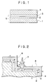
- Fig. 1 is a schematic partial cross-section to show an example of the construction of the electro-deposition coated member of the present invention.
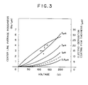
- Fig. 2 is a schematic partial cross-section to show an example of housings comprised of the electro-deposition coated member of the present invention.
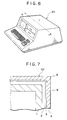
- Fig. 3 is a graph to show the relationship between center line average roughness (Ra) of the surface of an electro-deposition coating film and applied voltage, and the relationship between electro-deposition coating film thickness and applied voltage, for each average particle diameter of metallized ceramic powder.
- Fig. 4 is a graph to show the relationship between electromagnetic wave shielding performance and applied voltage for each average particle diameter, of an electro-deposition coated member having an electro-deposition coating film containing metallized ceramic powder.
- Fig. 5 is a graph to show the relationship between electromagnetic wave shielding performance and applied voltage for each average particle diameter, of an electro-deposition coated member having an electro-deposition coating film containing a mixed powder of metallized ceramic powder and ultrafine metal powder.
- Fig. 6 is a perspective illustration of a computer in which the electro-deposition coated member of the present invention is used to form a housing.
- Fig. 7 is a partial cross-section of the housing of the computer shown in Fig. 6.
- the electro-deposition coated member of the present invention is a member that forms a housing having on its surface a terraced portion or a vertically angular portion, where a plane portion and a corner of the terraced portion, or the vertically angular portion, of the housing are provided with an electro-deposition coating film containing conductive particles, thus giving a member provided with an exterior coating in a uniform thickness, almost free from any difference in coating film thickness between the corner of the terraced portion, or the vertically angular portion, and the plane portion of the housing.
- Fig. 1 is a schematic partial cross-section to show an example of the construction of the electro-deposition coated member of the present invention.
- the electro-deposition coated member of the present invention is a member that forms a housing having on its surface a terraced portion or a vertically angular portion.
- the corner of the terraced portion, or the vertically angular portion is provided with an exterior coating in the manner as shown in Fig. 1, in which a non-metal member 1 is provided thereon with a coating layer or plating layer 2 such as a metal copper thin film and a chemically colored film 3 is provided on the coating layer 2 to form a substrate layer 5, and an electro-deposition coating film 4 containing conductive particles is provided on the chemically colored film 3.
- Fig. 2 is a schematic partial cross-section to show an example of housings comprised of the electro-deposition coated member of the present invention.
- a plane portion 8, a corner 6 of a terraced portion and a vertically angular portion 7 of the housing are provided with an exterior coating comprised of the electro-deposition coating film containing conductive particles, where an exterior coating is formed in a uniform thickness, almost free from any difference in coating film thickness between the corner 6 of the terraced portion, or the vertically angular portion 7, and the plane portion 8 of the housing.
- the chemically colored film 3 can be formed by surface treatment of the metal thin film 2 formed on the substrate.
- the chemically colored film is preferable because it can improve the adhesion to the electro-deposition coating film to be formed thereon.
- this chemically colored film gives a good adhesion to the electro-deposition coating film, it can be presumed that the surface of the chemically colored film has a large number of very fine pores and hence a physical adsorption can be produced at the interface with the electro-deposition coating film and also a chemical adsorption is produced between functional groups of a polymer in the electro-deposition coating film, active points on the surfaces of the conductive particles, and the chemically colored film, thus giving a greatly superior adhesion.
- a chemically colored film formed by surface treatment of a copper thin film for example, a film comprised of cupric oxide, cuprous oxide, copper carbonate, copper sulfide or ammonium copper hydroxide can give an excellent adhesion to the electro-deposition coating film.
- the cupric oxide can be preferably used in view of the adhesion of the electro-deposition coating film to the substrate, the corrosion resistance of the metal thin film 2 and the uniformity of the electro-deposition coating film.
- a material other than copper is used as the metal substrate, it is preferred to apply copper plating to its surroundings.
- the metal thin film 2 is provided to form an electrode for the formation of the electro-deposition coating film and to form the chemically colored film on its surface. It may preferably have a film thickness of from 0.05 ⁇ m to 0.2 ⁇ m, and particularly from 0.1 ⁇ m to 0.15 ⁇ m. A film thickness larger than 0.2 ⁇ m is not preferred since it becomes necessary to take a long time for the formation of the copper thin film, resulting in an increase in the weight of the electro-deposition coated member and also a lowering of work efficiency.
- the chemically colored film can be prepared in the following way:
- the film comprised of cupric oxide can be formed, for example, by immersing a copper-plated substrate in a solution comprising a mixture of copper sulfide and potassium chlorate or a solution comprising a mixture of copper chloride, copper acetate and alum.
- the film comprised of copper sulfide can be formed, for example, by immersing the substrate in a solution comprising a mixture of potassium sulfide and ammonium chloride, or by immersing the substrate in a solution comprising a mixture of sodium hyposulfite and lead acetate.
- the film comprised of copper hydroxide can be formed, for example, by immersing the substrate in a solution comprising a mixture of copper nitrate, ammonium chloride and acetic acid.
- the film comprised of cuprous oxide, which is one of oxide films, can be formed, for example, by immersing the substrate in a solution comprising a mixture of copper sulfate and sodium chloride or a solution comprising a mixture of copper sulfate and ammonium chloride.
- the conductive electro-deposition coating film 4 is comprised of conductive particles deposited together with a resin feasible for electro-deposition, in a high density on the chemically colored film, has a conductivity even though it is a thin film, and functions as a coating film for electromagnetic wave shielding.
- the conductive particles to be deposited together with the resin to form the electro-deposition coating there are no particular limitations on the conductive particles to be deposited together with the resin to form the electro-deposition coating, so long as they can impart conductivity to the electro-deposition coating.
- They include, for example, a ceramic powder whose particle surfaces are coated with a metal (i.e., a metallized ceramic powder), a natural mica powder whose particles surfaces are coated with a metal (i.e., a metallized natural mica powder), an ultrafine metal powder having an average particle diameter of from 0.01 to 5 ⁇ m, a resin powder whose particles surfaces are coated with a metal, and a mixture of any of these.
- the metallized ceramic powder and the metallized natural mica powder are particularly preferred when the electro-deposition coating film is applied as a decorative coating film. This is because, when deposited together with the resin, they can facilitate complete curing of the electro-deposition coating at a low temperature of from 90 ° C to 100°C, which is usually required to be 130°C to 180°C as a heating temperature when the coating is cured by heat treatment after completion of electro-deposition, so that they enables achievement of firmer adhesion to the substrate.
- these metallized ceramic powder and metallized natural mica powder, or a mixture thereof have an excellent adhesion and can facilitate the low-temperature curing, it can be presumed that these powders are different from metal particles whose surfaces are susceptible to immediate oxidation, and can maintain the activity on the particle surfaces of the powder in a state stable to a certain extent by the mutual action between the particle surface and the metal coating, so that the active particle surfaces of the powder serve as cross-link points at the time of curing to accelerate the curing of the electro-deposition coating and also enable more formation of chemical bonds to the chemically colored film.
- the metallized ceramic powder or metallized natural mica powder used in the present invention may include a ceramic powder or natural mica powder whose particle surfaces are coated with Cu, Ni, Ag, Au, Sn or the like.
- Cu, Ag and Ni can be preferably used in view of the shielding performance and the cost.
- electroless plating As a method for the coating of the powder particle surfaces, it is suited to use electroless plating. A superior shielding performance and good coating film properties at the time of low-temperature curing can be obtained when the powder particle surfaces are coated in a coating thickness of from 0.05 ⁇ m to 3 ⁇ m, and particularly from 0.15 ⁇ m to 2 ⁇ m.
- coatings with a thickness of more than 3 ⁇ m makes the surface properties analogous to those of metal particles, so that the coatings are oxidized in the air because of their very active surfaces to bring about a decrease in the active points that contribute the cross-linking, tending to result in an insufficient curing of the electro-deposition coating at the time of low-temperature baking.
- Ni coatings are formed on the powder particles
- the method as disclosed, for example, in Japanese Patent Application Laid-open No. 61-276979 can be used, according to which a water-based suspension of the powder is prepared, and then an aged solution for electroless nickel plating is added to the suspension to form nickel coatings on the powder particle surfaces so that Ni coatings with a low phosphorus content, e.g., of 5 % or less can be applied.
- Ni coatings with a low phosphorus content e.g., of 5 % or less
- the ceramic powder and the natural mica powder may preferably have an average particle diameter of from 0.1 ⁇ m to 5 ⁇ m, particularly from 0.3 ⁇ m to 3 ⁇ m, and more preferably from 0.5 ⁇ m to 2 ⁇ m, taking account of the surface area contributory to its surface activity, the dispersibility in an electro-deposition coating composition, and a high-quality satin-like appearance of the coated member.
- the ceramic used in the present invention may include, for example, aluminum oxide, titanium nitride, manganese nitride, tungsten nitride, tungsten carbide, lanthanum nitride, aluminum silicate, molybdenum disulfide, titanium oxide and silica.
- the natural mica may include phlogopite, serisite and muscovite.
- the ultrafine metal powder having an average particle diameter of from 0.01 to 5 ⁇ m and a resin powder having an average particle diameter of from 0.1 to 5 ⁇ m whose particles surfaces are metallized.
- the ultrafine metal powder may include powders of Ag, Co, Cu, Fe, Mn, Ni, Pd, Sn, Te, etc. obtained by heat plasma evaporation, which may preferably have an average particle diameter ranging from 0.01 ⁇ m to 5 ⁇ m, particularly from 0.01 ⁇ m to 0.1 ⁇ m, and more preferably from 0.03 ⁇ m to 0.07 ⁇ m. Powder with an average particle diameter of less than 0.01 ⁇ m may cause secondary agglomeration.
- powder with an average particle diameter more than 5 ⁇ m may result in sedimentation of particles in an electro-deposition coating composition, and also may give a metallic gloss to a coated member, bringing about a difficulty in forming a coating in the desired color.
- the metallized resin powder also usable in the present invention can be obtained by forming Cu or Ni coatings in a thickness of from 0.05 ⁇ m to 3 ⁇ m as in the case of the ceramic powder, on powder particle surfaces of a resin including fluorine resins, polyethylene resins, acrylic resins, polystyrene resins and nylons.
- This resin powder may also preferably have an average particle diameter of from about 0.1 ⁇ m to about 5 ⁇ m.
- any of the conductive particles described above may be incorporated alone into the electro-deposition coating. It is thus possible to obtain an electro-deposition coated member with electromagnetic wave shielding properties and good coating film properties.
- the ultrafine metal powder or the metallized resin powder, or a mixture of these is added to the metallized ceramic powder or the metallized natural mica powder, or a mixture of these, in a weight proportion of the latter to the former of 1 : 0.2 to 3, the gaps between particles of the metallized ceramic powder and/or metallized natural mica powder in the electro-deposition coating are filled with particles of the ultrafine metal powder and/or metallized resin powder to increase contact areas between each powder, so that the shielding properties can be more improved and also an electro-deposition coated member having a superior coating film properties and a better adhesion to the substrate can be obtained even in the low-temperature heat treatment because of the action of the metallized ceramic powder and/or metallized natural mica powder.
- any resins conventionally used in electro-deposition coating can be used as the resin feasible for electro-deposition, including, for example, in the case of an anionic electro-deposition coating composition, a resin having an anionic functional group such as a carboxyl group in order to impart negative charges and hydrophilicity which are necessary for the electro-deposition of the resin, specifically including acrylic melamine resins, acrylic resins, alkyd resins, maleinized polybutadiene and half esters or half amides of these.
- the resin may include a resin having an cationic functional group such as an amino group in order to impart positive charges and hydrophilicity, specifically including epoxy resins, urethane resins, polyester resins and polyether resins.
- a resin having an cationic functional group such as an amino group in order to impart positive charges and hydrophilicity
- those having no self-crosslinking properties can be used in a mixture with a curing agent, for example, a melamine resin and a block polyisocyanate compound.
- the content (herein “deposition quantity”) of the conductive particles in the electro-deposition coating film of the present invention may preferably be in the range from 5 % by weight to 50 % by weight, particularly from 10 % by weight to 30 % by weight, and more preferably from 15 % by weight to 25 % by weight, in the electro-deposition coating film after curing.
- Such a content is preferred in order to attain an attenuation of, for example, 70 dB or more in the electromagnetic wave shielding performance and also taking account of the adhesion of the coating film as a decorative coating film to the substrate and the flexibility of the coating film.
- a content more than 50 % by weight may bring about a brittle coating film, which is unsuitable as an exterior coating film.
- a content less than 5 % by weight can give no sufficient shielding performance.
- the deposition quantity of the conductive particles can be measured by determination using an X-ray microanalyzer and by thermogravimetric analysis.
- the conductive particles are dispersed in the electro-deposition resin and deposited to form the electro-deposition coating film by the action of electrophoresis, so that a coating with a uniform coating thickness can be formed, which is almost free from any difference in coating film thickness between the corner of the terraced portion, or the vertically angular portion, and the plane portion of the housing.
- the magnetic wave shielding properties can be imparted to the housing by the exterior coating film.
- the curing reaction can well proceed in spite of a low-temperature heat treatment (100°C) and, in regard to coating film properties, it is possible to obtain the same properties as, or superior properties to, those of films formed by high-temperature curing.
- the electro-deposition coating film may have a surface roughness of from 0.3 ⁇ m to 5 ⁇ m, preferably from 0.5 ⁇ m to 4.0 ⁇ m, and more preferably from 0.7 ⁇ m to 3.0 ⁇ m, as the center line average roughness (Ra).
- a surface roughness less than 0.3 ⁇ m may cause a problem in decorativeness, namely, a difficulty in obtaining the satin-like appearance.
- a surface roughness more than 5 ⁇ m undesirably tends to result in a lowering of commercial value required as exterior coatings and also a lowering of coating film properties.
- metallic coating is applied to the non-metal substrate, and the chemically colored film is further formed.
- non-metal substrate any plastic materials used in plastic housings for office automation machinery, home electric appliances, etc. can be used, which include, for example, ABS resins, polycarbonate resins, polyetherimide resins, glass fiber packed ABS resins and glass fiber packed polycarbonate resins.
- the non-metal substrate is subjected to etching and a catalytic treatment, e.g., a palladium treatment is carried out, followed by formation of the metal thin film.
- a catalytic treatment e.g., a palladium treatment
- the formation of the metal thin film on the above non-metal substrate may preferably be carried out by electroless plating or electrolytic plating.
- This chemically colored film is formed on the metal thin film.
- This chemically colored film can be formed by chemical treatment of the surface of the metal thin film.
- a chemically colored film comprised of cupric oxide, copper carbonate, copper sulfide, ammonium copper hydroxide or cuprous oxide can be formed by a conventional method of treating a copper surface.
- a cupric oxide film capable of giving an excellent adhesion of the electro-deposition coating film is used as the chemically colored film, it can be obtained by an alkali treatment, e.g., by immersing a substrate with a copper thin film in an aqueous solution of sodium hydroxide.
- the copper may dissolve into an electro-deposition coating composition and accumulate therein to adversely affect coating film properties.
- the copper can be prevented from dissolving when the electro-deposition coating is formed on the copper oxide film, the chemically colored film, so that no copper ions can be present in the electro-deposition coating composition.
- this chemically colored film should be formed as a thin film.
- a substrate made of a metal can also be used as the substrate.
- Materials therefor include, for example, copper, iron, nickel, zinc and tin.
- the chemically colored film 3 can be formed by subjecting a substrate 5 to a direct surface treatment.
- a substrate made of a metal other than copper its surface may be plated with copper followed by an oxidation treatment, so that the chemically colored film comprised of copper oxide can be obtained. This is a preferred embodiment in view of an improvement in adhesion to the electro-deposition coating film 4.
- the substrate having been provided with the chemically colored film is immersed in an electro-deposition coating composition to carry out electro-deposition, thereby forming an electro-deposition coating on the chemically colored film.
- This electro-deposition process may be carried out according to a conventional method for electro-deposition coating.
- the electro-deposition may be carried out under conditions of a bath temperature ranging from 20°C to 25°C, an applied voltage of from 50 V to 200 V, a current density of from 0.5 A/dm 2 to 3 A/dm 2 , a treatment time ranging from 1 minute to 5 minutes to deposit together the resin and the conductive particles on the chemically colored film.
- the reason why the resin and the conductive particles are deposited together can be presumed as follows:
- functional groups bonded to the resin are ionized in the electro-deposition coating composition.
- the resin is attracted toward the article and thus deposited.
- this resin is adsorbed around the conductive particles.
- the conductive particles are also moved and thus deposited on the article together with the resin.
- the above substrate thus provided with an electro-deposition coating is washed with water and then heated to effect curing of the coating.
- the above curing may be carried out in an oven at a low temperature of from 90°C to 100°C for 20 minutes to 180 minutes, so that sufficient curing can be effected.
- the heating should be carried out at about 120°C to about 180°C.
- the electro-deposition coated member can be obtained to which the electromagnetic wave shielding properties have been imparted and at the same time an exterior coating has been applied.
- the electro-deposition coating film may preferably be formed as thinly as possible so long as the shielding properties can be ensured, and specifically may preferably be formed in a thickness of from 7 ⁇ m to 40 ⁇ m, and particularly from 10 ⁇ m to 25 ⁇ m.
- Fig. 3 shows the relationship between center line average roughness (Ra) of the surface of an electro-deposition coated member and applied voltage, and the relationship between electro-deposition coating film thickness and applied voltage, obtained when a housing with the substrate layer 5 formed thereon was immersed in an electro-deposition coating composition prepared by dispersing, in 100 parts by weight of an acrylic melamine resin (trade name: Honey Bright C-IL; produced by Honey Chemical Co.), 15 parts by weight of an alumina powder with an average particle diameter of 0.5 ⁇ m, 1 ⁇ m, 3 ⁇ m or 5 ⁇ m whose particle surfaces were coated with copper by electroless plating in a thickness of 0.1 ⁇ m and diluting the dispersion to 15 % by weight as a concentration of solid contents, and electro-deposition was carried out for 3 minutes at an applied voltage of varied volts.
- an acrylic melamine resin trade name: Honey Bright C-IL; produced by Honey Chemical Co.
- the surface roughness becomes greater with an increase in the applied voltage under the same average particle diameter.
- the deposition quantity of the conductive particles in the electro-deposition coating film was about 25 % by weight at a voltage of, for example, 100 V, without regard to the average particle diameter.
- Fig. 4 is a graph to show the relationship between a voltage and a mean value (dB) of attenuations against electromagnetic waves of 50 to 1,000 MHz, with respect to the average particle diameter ( ⁇ m) of the conductive particles.
- the shielding effect increases with an increase in the voltage. It is also seen that the shielding effect is in inverse proportion to the average particle diameter. This is presumably due to the fact that under the same voltage the deposition quantity in the electro-deposition coating film is constant without regard to the particle size and hence, with an increase in the average particle diameter, the relative number of the conductive particles in the electro-deposition coating film decreases and the contact areas between particles decrease.
- a metallized ceramic powder with an average particle diameter of 0.5 ⁇ m may be used under application of a voltage of 200 V or a metallized ceramic powder with an average particle diameter of 1 ⁇ m may be used under application of a voltage of 125 V.
- the surface roughness of the electro-deposition coated member obtained is predominantly influenced by the powder with a larger average particle diameter and the deposition quantity thereof.
- the Ra depends on the proportion of the metallized alumina powder held in the total deposition quantity in the electro-deposition coating film.
- the metallized alumina powder is deposited in a quantity of 10 % by weight and an electro-deposition coated member having the surface roughness as shown in Fig. 3 by a dotted line can be obtained.
- the shielding performance can be improved as previously stated.
- an electro-deposition coating composition prepared by dispersing, in 100 parts parts by weight of an acrylic melamine resin, 10 parts by weight of an alumina powder with an average particle diameter of 0.5 ⁇ m, 1 urn, 3 ⁇ m or 5 ⁇ m whose particle surfaces are coated with copper in a thickness of 0.1 ⁇ m and 15 parts by weight of a copper powder with an average particle diameter of 0.05 ⁇ m and diluting the dispersion to 15 % by weight as a concentration of solid contents, to form an electro-deposition coated member having an electro-deposition coating film of 20 ⁇ m in coating thickness and 30 % by weight in deposition quantity, the shielding performance is as shown in Fig. 5. It is seen therefrom that the shielding effect has been more improved than the case shown in Fig. 4.
- the desired degree of satin finishing and the desired electromagnetic wave shielding performance can be achieved by varying the particle diameter of the conductive particles, the applied voltage and the content of the conductive particles in the electro-deposition coating composition.
- a decorative coating can be formed on the surface of a housing and also electromagnetic wave shielding properties can be imparted to the housing, when the present invention is used for exterior coating of a housing 101 of, for example, the electronic machinery as shown in Figs. 6 and 7.
- the surface of the housing having on its surface a terraced portion or a vertically angular portion is provided with the electro-deposition coating film containing the conductive particles, and thus an exterior coating can be formed in a uniform thickness, almost free from any difference in coating film thickness between the corner of the terraced portion, or the vertically angular portion, and the plane portion of the housing, and also the surface of the housing can be finished in a uniformly satin-finished surface, bringing about a remarkable improvement in the decorative appearance.
- the present invention can make a great contribution to exterior coating and also to economical advantages.
- the electromagnetic wave shielding properties can be imparted to the electro-deposition coating film, and also the electromagnetic wave shielding and the exterior coating can be carried out in one step.
- the electromagnetic wave shielding properties and the degree of satin finishing on the housing surface can be arbitrarily controlled by changing the content of the conductive particles in the electro-deposition coating, the particle diameter, the applied voltage and the electro-deposition time, so that it is possible to carry out the coating according to the purpose for which the housings to be coated are used.
- the particle size of powder is measured with a centrifugal sedimentation particle size distribution measuring device (trade name: SACP-3; manufactured by Shimadzu Corporation). All powders are deemed to be comprised of dense spheres having the same particle diameters.
- thermogravimetric analyzer (trade name: Thermal Analysis System 7 series; manufactured by Perkin-Elmer Co.).
- the electromagnetic wave shielding performance is measured according to the transmission line method (ASTM ES7-83 Method).
- a sensitizer solution a solution comprised of 30 g/lit. of stannous chloride and 20 ml/lit. of hydrochloric acid and washed with water.
- an activator solution a solution comprised of 0.3 g/lit. of
- an acrylic melamine resin (trade name: Honey Bright C-IL; produced by Honey Chemical Co.)
- 15 parts by weight of alumina with an average particle diameter of 1 ⁇ m whose particle surfaces were coated with nickel by electroless plating in a thickness of 0.2 ⁇ m was dispersed for 30 hours using a ball mill, and then the dispersion was diluted with desalted water to 15 % by weight as a concentration of solid contents, followed by further addition of 2.0 % by weight of carbon black for the purpose of coloring to make up a coating composition.
- electro-deposition was carried out at an applied voltage of 120 V for 3 minutes under conditions of a bath temperature of 25°C and pH 8 to 9, setting the article to be coated as the anode and a 0.5t stainless steel sheet as the opposing electrode. After the electro-deposition, the coated article was washed with water and then heated in an oven of 97°C ⁇ 1°C for 60 minutes to effect curing. An electro-deposition coated member was thus obtained, having an electro-deposition coating film of 25 ⁇ m in coating thickness, containing 20 % by weight (deposition quantity) of metallized alumina powder.
- Thickness distribution of the electro-deposition coating film was also measured using a metallurgical microscope manufactured by Olympus Optical Co., Ltd., throughout the cross section of a to w shown in Fig. 2. Results obtained are shown in Table 1-1. As shown in the table, the coating film had been uniformly formed in a thickness within the range of from 24.7 ⁇ m to 26.0 ⁇ m at the terraced and vertically angular portions, where the coating thickness was almost the same as that of the plane portion 8.
- the center line average roughness (Ra) of the surface of this electro-deposition coating film was 1.0 ⁇ m.
- the center line average roughness (Ra) of the surface was measured using Talysurf Type-6, manufactured by Rank Taylor Hobson Co.
- Electromagnetic wave shielding performance against electromagnetic waves with frequencies of from 50 to 1,000 MHz was also measured according to the transmission line method to reveal that the attenuation was as good as about 80 dB.
- Example 1-1 The surface of the ABS resin housing as used in Example 1-1 was coated with copper by electroless plating in a thickness of 0.7 ⁇ m, followed by the same treatments as in Example 1-1 to give an electro-deposition coated member having an electro-deposition coating film of 20 ⁇ m in coating thickness, containing 20 % by weight of metallized alumina powder.
- Example 1-1 The surface of the ABS resin housing as used in Example 1-1 was coated with copper by electroless plating in a thickness of 0.7 ⁇ m and subsequently coated with nickel by electroless plating in a thickness of 0.3 ⁇ m, followed by the same treatments as in Example 1-1 to give an electro-deposition coated member having an electro-deposition coating film of 20 ⁇ m in coating thickness, containing 20 % by weight of metallized alumina powder.
- Electro-deposition coating was carried out in the same manner as in Example except that the metallized alumina powder used therein was not added.
- the electro-deposition coated member thus obtained was evaluated in the same manner as in Example 1-1 to reveal that as to the electromagnetic wave shielding performance the attenuation was less than 50 dB.
- the appearance of the coating film and the coating film properties were as shown in Tables 1-2 and 1-3, showing that it was impossible to effect satin finishing of the housing surface and therefore the coating film was unsuitable as a satin-like decorative coating and an electromagnetic wave shielding coating.
- Example 1-1 To 50 g of an acrylic coating composition (No. 2026; produced by Kansai Paint Co., Ltd.), 50 g of the metallized alumina powder as used in Example 1-1 was added, which were gently mixed by the aid of a toluene solvent, followed by stirring for 10 minutes using a homomixer to give a spray coating composition.
- an acrylic coating composition No. 2026; produced by Kansai Paint Co., Ltd.
- Example 1-1 the ABS resing housing as used in Example 1-1 was spray-coated with the above spray coating composition to give a coated member having a spray coating film of 40 ⁇ m in dried coating thickness.
- This member was evaluated in the same manner as in Example 1-1 to reveal that the coating thickness at the terraced portion or vertically angular portion was not less than 5 ⁇ m smaller than that at the plane portion 8 and as for the electromagnetic wave shielding performance the attenuation was not more than 50 dB.
- the quality of appearance (uniformity, lack of hiding, stains, gloss unveness, runs, foreign matters, and degree of satin finishing), coating film properties (adhesion, moisture resistance, accelerated light-resistance, salt spray resistance, pencil hardness, alkali resistance, and solvent resistance) and electromagnetic wave shielding performance of the coating films of Examples 1-1 to 1-3 and Comparative Examples 1 and 2 were evaluated to obtain the results as shown in Tables 1-2 and 1-3.
- a sensitizer solution a solution comprised of 30 g/lit. of stannous chloride and 20 ml/lit. of hydrochloric acid and washed with water.
- an activator solution a solution comprised of 0.3 g/lit. of
- an acrylic melamine resin (trade name: Honey Bright C-IL; produced by Honey Chemical Co.)
- 15 parts by weight of silicon carbide with an average particle diameter of 1 ⁇ m whose particle surfaces were coated with copper by electroless plating in a thickness of 0.2 ⁇ m was dispersed for 30 hours using a ball mill, and then the dispersion was diluted with desalted water to 15 % by weight as a concentration of solid contents, followed by further addition of 2.0 % by weight of carbon black for the purpose of coloring to make up a coating composition.
- electro-deposit ion was carried out at an applied voltage of 150 V for 3 minutes under conditions of a bath temperature of 25°C and pH 8 to 9, setting the article to be coated as the anode and a 0.5t stainless steel sheet as the opposing electrode.
- the coated article was washed with water and then heated in an oven of 97°C ⁇ 1°C for 60 minutes to effect curing.
- An electro-deposition coated member was thus obtained, having an electro-deposition coating film of 25 ⁇ m in coating thickness, containing 30 % by weight of metallized silicon carbide powder.
- Example 1-1 In respect of this electro-deposition coated member, the appearance of its coating film was evaluated and its coating film properties were measured, according to JIS K5980 as in Example 1-1. As a result, the same results as those in Example 1-1 were obtained.
- Thickness distribution of the electro-deposition coating film was also measured in the same manner as in Example 1-1 to reveal that, like Example 1-1, the coating film had been uniformly formed at the terraced and vertically angular portions, where the coating thickness was almost the same as that of the plane portion 8.
- the center line average roughness (Ra) of the surface of this electro-deposition coating film was 1.5 ⁇ m. Electromagnetic wave shielding performance was also measured in the same manner as in Example 1-1 to reveal that the attenuation was about 85 dB. As a result of this evaluation, the present invention was confirmed to be applicable to high-quality satin-like exterior coating and to electromagnetic wave shielding coating.
- a sensitizer solution a solution comprised of 30 g/lit. of stannous chloride and 20 ml/lit. of hydrochloric acid and washed with water.
- an activator solution a solution comprised of 0.3 g/lit. of
- an acrylic melamine resin (trade name: Honey Bright C-IL; produced by Honey Chemical Co.)
- 15 parts by weight of alumina with an average particle diameter of 0.5 ⁇ m whose particle surfaces were coated with nickel by electroless plating in a thickness of 0.2 ⁇ m was dispersed for 30 hours using a ball mill, and then the dispersion was diluted with desalted water to 15 % by weight as a concentration of solid contents, followed by further addition of 2.0 % by weight of carbon black for the purpose of coloring to make up a coating composition.
- electro-deposition was carried out at an applied voltage of 120 V for 3 minutes under conditions of a bath temperature of 25°C and pH 8 to 9, setting the article to be coated as the anode and a 0.5t stainless steel sheet as the opposing electrode.
- the coated article was washed with water and then heated in an oven of 97°C ⁇ 1°C for 60 minutes to effect curing.
- An electro-deposition coated member was thus obtained, having an electro-deposition coating film of 20 ⁇ m in coating thickness, containing 22 % by weight, as deposition quantity, of metallized alumina powder.
- Example 1-1 the appearance of its coating film was evaluated and its coating film properties were measured, according to JIS K5980 as in Example 1-1. As a result, the same results as those in Example 1-1 were obtained, which were of the same level as, or a higher level than, that of a conventional high-temperature baked coating formed on a metal.
- Thickness distribution of the electro-deposition coating film was also measured in the same manner as in Example 1-1 to reveal that, like Example 1-1, the coating film had been uniformly formed at the terraced and vertically angular portions, where the coating thickness was almost the same as that of the plane portion 8.
- the center line average roughness (Ra) of the surface of this electro-deposition coating film was 0.5 ⁇ m. Electromagnetic wave shielding performance was also measured to reveal that the attenuation was about 88 dB. As a result of this evaluation, the present invention was confirmed to be applicable to exterior coating and to electromagnetic wave shielding coating.
- a sensitizer solution a solution comprised of 30 g/lit. of stannous chloride and 20 ml/lit. of hydrochloric acid and washed with water.
- an activator solution a solution comprised of 0.3 g/lit. of palladium chloride and 3
- an acrylic melamine resin (trade name: Honey Bright C-IL; produced by Honey Chemical Co.)
- 15 parts by weight of silicon carbide with an average particle diameter of 5 ⁇ m whose particle surfaces were coated with copper by electroless plating in a thickness of 0.2 ⁇ m was dispersed for 30 hours using a ball mill, and then the dispersion was diluted with desalted water to 15 % by weight as a concentration of solid contents, followed by further addition of 2.0 % by weight of carbon black for the purpose of coloring to make up a coating composition.
- electro-deposition was carried out at an applied voltage of 170 V for 3 minutes under conditions of a bath temperature of 25°C and pH 8 to 9, setting the article to be coated as the anode and a 0.5t stainless steel sheet as the opposing electrode.
- the coated article was washed with water and then heated in an oven of 97°C ⁇ 1°C for 60 minutes to effect curing.
- An electro-deposition coated member was thus obtained, having an electro-deposition coating film of 28 ⁇ m in coating thickness, containing 35 % by weight of metallized silicon carbide powder.
- Example 1-1 the appearance of its coating film was evaluated and its coating film properties were measured, according to JIS K5980 as in Example 1-1. As a result, the same results as those in Example 1-1 were obtained, which were of the same level as, or a higher level than, that of a conventional high-temperature baked coating formed on a metal.
- Thickness distribution of the electro-deposition coating film was also measured in the same manner as in Example 1-1 to reveal that, like Example 1-1, the coating film had been uniformly formed at the terraced and vertically angular portions, where the coating thickness was almost the same as that of the plane portion.
- the center line average roughness (Ra) of the surface of this electro-deposition coating film was 5 ⁇ m. Electromagnetic wave shielding performance was also measured to reveal that the attenuation was about 70 dB. As a result of this evaluation, the present invention was confirmed to be applicable to exterior coating and to electromagnetic wave shielding coating.
- a sensitizer solution a solution comprised of 30 g/lit. of stannous chloride and 20 ml/lit. of hydrochloric acid and washed with water.
- an activator solution a solution comprised of 0.3 g/lit. of
- an acrylic melamine resin (trade name: Honey Bright C-IL; produced by Honey Chemical Co.)
- 10 parts by weight of a copper powder with an average particle diameter of 0.03 ⁇ m and 8 parts by weight of alumina with an average particle diameter of 1 ⁇ m whose particle surfaces were coated with copper by electroless plating in a thickness of 0.2 ⁇ m were dispersed for 30 hours using a ball mill, and then the dispersion was diluted with desalted water to 15 % by weight as a concentration of solid contents, followed by further addition of 2.0 % by weight of carbon black for the purpose of coloring to make up a coating composition.
- electro-deposition was carried out at an applied voltage of 150 V for 3 minutes under conditions of a bath temperature of 25°C and pH 8 to 9, setting the article to be coated as the anode and a 0.5t stainless steel sheet as the opposing electrode. After the electro-deposition, the coated article was washed with water and then heated in an oven of 97°C ⁇ 1°C for 60 minutes to effect curing. An electro-deposition coated member was thus obtained, having an electro-deposition coating film of 25 ⁇ m in coating thickness, containing 30 % by weight of metallized alumina powder and copper powder.
- Thickness distribution of the electro-deposition coating film was also measured using a metallurgical microscope manufactured by Olympus Optical Co., Ltd., throughout the cross section of a to w shown in Fig. 2, in the same manner as in Example 1-1. As a result, scattering of the coating thickness was within ⁇ 4 %.
- the center line average roughness (Ra) of the surface of this electro-deposition coating film was 1.0 ⁇ m. Electromagnetic wave shielding performance was also measured in the same manner as in Example 1-1 to reveal that the attenuation was about 90 dB or more, which was evaluated as "AA". As a result of this evaluation, the present invention was confirmed to be applicable to exterior coating capable of providing a high-quality satin-like appearance and to electromagnetic wave shielding coating.
- a sensitizer solution a solution comprised of 30 g/lit. of stannous chloride and 20 ml/lit. of hydrochloric acid and washed with water.
- an activator solution a solution comprised of 0.3 g/lit. of
- an acrylic melamine resin (trade name: Honey Bright C-IL; produced by Honey Chemical Co.)
- 7 parts by weight of a copper powder with an average particle diameter of 0.05 ⁇ m and 8 parts by weight of silicon carbide with an average particle diameter of 1 ⁇ m whose particle surfaces were coated with copper by electroless plating in a thickness of 0.2 ⁇ m were dispersed for 30 hours using a ball mill, and then the dispersion was diluted with desalted water to 15 % by weight as a concentration of solid contents, followed by further addition of 2.0 % by weight of carbon black for the purpose of coloring to make up a coating composition.
- electro-deposition was carried out at an applied voltage of 120 V for 3 minutes under conditions of a bath temperature of 25°C and pH 8 to 9, setting the article to be coated as the anode and a 0.5t stainless steel sheet as the opposing electrode. After the electro-deposition, the coated article was washed with water and then heated in an oven of 97°C ⁇ 1°C for 60 minutes to effect curing. An electro-deposition coated member was thus obtained, having an electro-deposition coating film of 20 ⁇ m in coating thickness, containing 20 % by weight of the powder mixture.
- Example 1-1 In respect of this electro-deposition coated member, the appearance of its coating film was evaluated and its coating film properties were measured, according to JIS K5980 as in Example 1-1. As a result, the same results as those in Example 1-1 were obtained.
- Thickness distribution of the electro-deposition coating film was also measured in the same manner as in Example 1-1 to reveal that, like Example 2-1, the coating film had been uniformly formed at the terraced and vertically angular portions, where the coating thickness was almost the same as that of the plane portion 8.
- the center line average roughness (Ra) of the surface of this electro-deposition coating film was 0.7 ⁇ m. Electromagnetic wave shielding performance was also measured to reveal that the attenuation was 90 dB or more. As a result of this evaluation, the present invention was confirmed to be applicable to exterior coating capable of providing high-quality satin-like appearance and to electromagnetic wave shielding coating.
- a sensitizer solution a solution comprised of 30 g/lit. of stannous chloride and 20 ml/lit. of hydrochloric acid and washed with water.
- an activator solution a solution comprised of 0.3 g/lit. of
- an acrylic melamine resin (trade name: Honey Bright C-IL; produced by Honey Chemical Co.)
- 3 parts by weight of a silver powder with an average particle diameter of 0.07 ⁇ m and 7 parts by weight of alumina with an average particle diameter of 0.2 ⁇ m whose particle surfaces were coated with nickel by electroless plating in a thickness of 0.2 ⁇ m were dispersed for 30 hours using a ball mill, and then the dispersion was diluted with desalted water to 15 % by weight as a concentration of solid contents, followed by further addition of 2.0 % by weight of carbon black for the purpose of coloring to make up a coating composition.
- electro-deposition was carried out at an applied voltage of 120 V for 3 minutes under conditions of a bath temperature of 25°C and pH 8 to 9, setting the article to be coated as the anode and a 0.5t stainless steel sheet as the opposing electrode. After the electro-deposition, the coated article was washed with water and then heated in an oven of 97°C ⁇ 1°C for 60 minutes to effect curing. An electro-deposition coated member was thus obtained, having an electro-deposition coating film of 20 ⁇ m in coating thickness, containing 30 % by weight of the powder mixture.
- Example 2-1 In respect of this electro-deposition coated member, the appearance of its coating film was evaluated and its coating film properties were measured, according to JIS K5980 as in Example 1-1. As a result, the same results as those in Example 2-1 were obtained.
- Thickness distribution of the electro-deposition coating film was also measured in the same manner as in Example 1-1 to reveal that, like Example 2-1, the coating film had been uniformly formed at the terraced and vertically angular portions, where the coating thickness was almost the same as that of the plane portion 8.
- the center line average roughness (Ra) of the surface of this electro-deposition coating film was 0.3 ⁇ m. Electromagnetic wave shielding performance was also measured to reveal that the attenuation was 90 dB or more, which was evaluated as "AA". As a result of this evaluation, the present invention was confirmed to be applicable to exterior coating capable of providing fine satin-like appearance and to electromagnetic wave shielding coating.
- a sensitizer solution a solution comprised of 30 g/lit. of stannous chloride and 20 ml/lit. of hydrochloric acid and washed with water.
- an activator solution a solution comprised of 0.3 g/lit. of
- an acrylic melamine resin (trade name: Honey Bright C-IL; produced by Honey Chemical Co.)
- 5 parts by weight of a nickel powder with an average particle diameter of 0.03 ⁇ m and 5 parts by weight of silicon carbide with an average particle diameter of 0.5 ⁇ m whose particle surfaces were coated with copper by electroless plating in a thickness of 0.2 ⁇ m were dispersed for 30 hours using a ball mill, and then the dispersion was diluted with desalted water to 15 % by weight as a concentration of solid contents, followed by further addition of 2.0 % by weight of carbon black for the purpose of coloring to make up a coating composition.
- electro-deposition was carried out at an applied voltage of 200 V for 3 minutes under conditions of a bath temperature of 25°C and pH 8 to 9, setting the article to be coated as the anode and a 0.5t stainless steel sheet as the opposing electrode. After the electro-deposition, the coated article was washed with water and then heated in an oven of 97°C ⁇ 1°C for 60 minutes to effect curing. An electro-deposition coated member was thus obtained, having an electro-deposition coating film of 30 ⁇ m in coating thickness, containing 30 % by weight of the powder mixture.
- Example 2-1 In respect of this electro-deposition coated member, the appearance of its coating film was evaluated and its coating film properties were measured, according to JIS K5980 as in Example 1-1. As a result, the same results as those in Example 2-1 were obtained.
- Thickness distribution of the electro-deposition coating film was also measured in the same manner as in Example 1-1 to reveal that, like Example 2-1, the coating film had been uniformly formed at the terraced and vertically angular portions, where the coating thickness was almost the same as that of the plane portion 8.
- the center line average roughness (Ra) of the surface of this electro-deposition coating film was 0.5 ⁇ m.
- Electromagnetic wave shielding performance was also evaluated in the same manner as in Example 3-1 to reveal that the attenuation was 100 dB or more. As a result of this evaluation, the present invention was confirmed to be applicable to exterior coating capable of providing satin-like appearance and to electromagnetic wave shielding coating.
- a sensitizer solution a solution comprised of 30 g/lit. of stannous chloride and 20 ml/lit. of hydrochloric acid and washed with water.
- an activator solution a solution comprised of 0.3 g/lit. of
- an acrylic melamine resin (trade name: Honey Bright C-IL; produced by Honey Chemical Co.)
- 15 parts by weight of a natural mica powder with an average particle diameter of 2.0 ⁇ m whose particle surfaces were coated with copper by electroless plating in a thickness of 0.05 ⁇ m was dispersed for 30 hours using a ball mill, and then the dispersion was diluted with desalted water to 15 % by weight as a concentration of solid contents, followed by further addition of 2.0 % by weight of carbon black for the purpose of coloring to make up a coating composition.
- electro-deposition was carried out at an applied voltage of 120 V for 3 minutes under conditions of a bath temperature of 25°C and pH 8 to 9, setting the article to be coated as the anode and a 0.5t stainless steel sheet as the opposing electrode. After the electro-deposition, the coated article was washed with water and then heated in an oven of 97°C ⁇ 1°C for 60 minutes to effect curing. An electro-deposition coated member was thus obtained, having an electro-deposition coating film of 20 ⁇ m in coating thickness, containing 20 % by weight of the powder mixture.
- Example 1-1 In respect of this electro-deposition coated member, the appearance of its coating film was evaluated and its coating film properties were measured, according to JIS K5980 as in Example 1-1. As a result, the results as shown in Tables 3-1 and 3-2 were obtained, which were of the same level as, or a higher level than, those in Example 1-1.
- Thickness distribution of the electro-deposition coating film was also measured in the same manner as in Example 1-1 to reveal that scattering of the coating thickness was within ⁇ 4 % and the coating film had been uniformly formed also at the terraced and vertically angular portions, where the coating thickness was almost the same as that of the plane portion 8.
- the center line average roughness (Ra) of the surface of this electro-deposition coating film was 1.4 ⁇ m.
- the attenuation was about 75 dB. From these results, the present invention was confirmed to be applicable to exterior coating capable of providing high-quality satin-like appearance and to electromagnetic wave shielding coating.
- a coating composition was prepared in the following way: In 100 parts by weight of an acrylic melamine resin (trade name: Honey Bright C-IL; produced by Honey Chemical Co.), 5 parts by weight of a nickel powder with an average particle diameter of 0.03 ⁇ m and 10 parts by weight of a natural mica powder with an average particle diameter of 1.5 ⁇ m whose particle surfaces were coated with nickel by electroless plating in a thickness of 0.2 ⁇ m were dispersed for 30 hours using a ball mill, and then the dispersion was diluted with desalted water to 15 % by weight as a concentration of solid contents, followed by further addition of 2.0 % by weight of carbon black for the purpose of coloring.
- an acrylic melamine resin trade name: Honey Bright C-IL; produced by Honey Chemical Co.
- electro-deposition was carried out at an applied voltage of 150 V for 3 minutes under conditions of a bath temperature of 25°C and pH 8 to 9, setting the article to be coated as the anode and a 0.5t stainless steel sheet as the opposing electrode. After the electro-deposition, the coated article was washed with water and then heated in an oven of 97°C ⁇ 1°C for 60 minutes to effect curing. An electro-deposition coated member was thus obtained, having an electro-deposition coating film of 24 ⁇ m in coating thickness, containing 28 % by weight of the powder mixture.
- Thickness distribution of the electro-deposition coating film was also measured in the same manner as in Example 1-1 to reveal that, like Example 3-1, the coating film had been uniformly formed at the terraced and vertically angular portions, where the coating thickness was almost the same as that of the plane portion 8.
- the center line average roughness (Ra) of the surface of this electro-deposition coating film was 2 ⁇ m. Electromagnetic wave shielding performance was also measured to reveal that the attenuation was 100 dB or more. As a result of this evaluation, the present invention was confirmed to be applicable to exterior coating capable of providing high-quality satin-like appearance and to electromagnetic wave shielding coating.
- a sensitizer solution a solution comprised of 30 g/lit. of stannous chloride and 20 ml/lit. of hydrochloric acid and washed with water.
- an activator solution a solution comprised of 0.3 g/lit. of
- a coating composition was prepared in the following way: In 100 parts by weight of an acrylic melamine resin (trade name: Honey Bright C-IL; produced by Honey Chemical Co.), 3 parts by weight of a silver powder with an average particle diameter of 0.07 ⁇ m, 7 parts by weight of alumina with an average particle diameter of 0.2 ⁇ m whose particle surfaces were coated with nickel by electroless plating in a thickness of 0.2 ⁇ m, and 10 parts by weight of a natural mica powder with an average particle diameter of 1.5 ⁇ m whose particle surfaces were coated with nickel by electroless plating in a thickness of 0.02 ⁇ m were dispersed for 30 hours using a ball mill, and then the dispersion was diluted with desalted water to 15 % by weight as a concentration of solid contents, followed by further addition of 2.0 % by weight of carbon black for the purpose of coloring.
- an acrylic melamine resin trade name: Honey Bright C-IL; produced by Honey Chemical Co.
- electro-deposition was carried out at an applied voltage of 100 V for 3 minutes under conditions of a bath temperature of 25°C and pH 8 to 9, setting the article to be coated as the anode and a 0.5t stainless steel sheet as the opposing electrode. After the electro-deposition, the coated article was washed with water and then heated in an oven of 97°C ⁇ 1°C for 60 minutes to effect curing. An electro-deposition coated member was thus obtained, having an electro-deposition coating film of 16 ⁇ m in coating thickness, containing 15 % by weight of the powder mixture.
- Thickness distribution of the electro-deposition coating film was also measured in the same manner as in Example 1-1 to reveal that the coating film had been uniformly formed at the terraced and vertically angular portions, where the coating thickness was almost the same as that of the plane portion 8.
- the center line average roughness (Ra) of the surface of this electro-deposition coating film was 0.8 ⁇ m.
- the attenuation was about 90 dB. From these results, the present invention was confirmed to be applicable to exterior coating capable of providing high-quality satin-like appearance and to electromagnetic wave shielding coating.
- a sensitizer solution a solution comprised of 30 g/lit. of stannous chloride and 20 ml/lit. of hydrochloric acid and washed with water.
- an activator solution a solution comprised of 0.3 g/lit. of
- a coating composition was prepared in the following way: In 100 parts by weight of an acrylic melamine resin (trade name: Honey Bright C-IL; produced by Honey Chemical Co.), 15 parts by weight of a silicon carbide with an average particle diameter of 0.5 ⁇ m whose particle surfaces were coated with copper by electroless plating in a thickness of 0.2 ⁇ m and 15 parts by weight of a natural mica powder with an average particle diameter of 3 ⁇ m whose particle surfaces were coated with copper by electroless plating in a thickness of 0.2 ⁇ m were dispersed for 30 hours using a ball mill, and then the dispersion was diluted with desalted water to 15 % by weight as a concentration of solid contents, followed by further addition of 2.0 % by weight of carbon black for the purpose of coloring.
- an acrylic melamine resin trade name: Honey Bright C-IL; produced by Honey Chemical Co.
- electro-deposition was carried out at an applied voltage of 170 V for 3 minutes under conditions of a bath temperature of 25°C and pH 8 to 9, setting the article to be coated as the anode and a 0.5t stainless steel sheet as the opposing electrode.
- the coated article was washed with water and then heated in an oven of 97°C ⁇ 1°C for 60 minutes to effect curing.
- An electro-deposition coated member was thus obtained, having an electro-deposition coating film of 27 ⁇ m in coating thickness, containing 35 % by weight of the powder mixture.
- Thickness distribution of the electro-deposition coating film was also measured in the same manner as in Example 1-1 to reveal that scattering of the coating thickness was within ⁇ 10 % and the coating film had been uniformly formed at the terraced and vertically angular portions, where the coating thickness was almost the same as that of the plane portion 8.
- a sensitizer solution a solution comprised of 30 g/lit. of stannous chloride and 20 ml/lit. of hydrochloric acid and washed with water.
- an activator solution a solution comprised of 0.3 g/lit. of
- plating was carried out at a bath temperature of 70°C for 3 minutes to form a copper thin film of 0.2 ⁇ m thickness.
- a solution comprising a mixture of copper sulfate and sodium chloride, the surface of the copper thin film was treated at 70°C for 30 seconds to form a cuprous oxide film, the chemically colored film.
- an acrylic melamine resin (trade name: Honey Bright C-IL; produced by Honey Chemical Co.) 15 parts by weight of a copper powder with an average particle diameter of 0.02 ⁇ m was dispersed for 30 hours using a ball mill, and then the dispersion was diluted with desalted water to 15 % by weight as a concentration of solid contents, followed by further addition of 2.0 % by weight of carbon black for the purpose of coloring to make up a coating composition.
- electro-deposition was carried out at an applied voltage of 200 V for 3 minutes under conditions of a bath temperature of 25°C and pH 8 to 9, setting an article to be coated as the anode and a 0.5t stainless steel sheet as the opposing electrode.
- the coated article was washed with water and then heated in an oven of 145°C ⁇ 1°C for 60 minutes to effect curing.
- An electro-deposition coated member was thus obtained, having an electro-deposition coating film of 27 ⁇ m in coating thickness, containing 38 % by weight of the powder.
- Thickness distribution of the electro-deposition coating film was also measured using a metallurgical microscope manufactured by Olympus Optical Co., Ltd., throughout the cross section of a to w shown in Fig. 2. As a result, the coating film had been uniformly formed at the terraced and vertically angular portions, where the coating thickness was almost the same as that of the plane portion 8.
- the center line average roughness (Ra) of the surface of this electro-deposition coating film was 0.3 ⁇ m.
- the center line average roughness (Ra) of the surface was measured using Talysurf Type-6, manufactured by Rank Taylor Hobson Co.
Landscapes
- Chemical & Material Sciences (AREA)
- Materials Engineering (AREA)
- Life Sciences & Earth Sciences (AREA)
- Organic Chemistry (AREA)
- Engineering & Computer Science (AREA)
- Wood Science & Technology (AREA)
- Health & Medical Sciences (AREA)
- Molecular Biology (AREA)
- Chemical Kinetics & Catalysis (AREA)
- Electrochemistry (AREA)
- Metallurgy (AREA)
- Shielding Devices Or Components To Electric Or Magnetic Fields (AREA)
- Other Surface Treatments For Metallic Materials (AREA)
Claims (23)
- Gehäuse mit einer Oberfläche, die einen terrassierten Teil und/oder einen vertikal abgewinkelten Teil aufweist,
dadurch gekennzeichnet, daß
das Gehäuse versehen ist mit einer leitenden Elektroniederschlagsbeschichtung in gleichförmiger Dicke sowie praktisch frei von jeglichem Unterschied in der Schichtdicke zwischen einer Ecke des terrassierten Teils oder des vertikal abgewinkelten Teils und einem ebenen Teil des Gehäuses, wobei die Beschichtung ein leitendes Pulver aus metallisiertem Keramikpulver, metallisiertem Glimmerpulver oder Mischungen davon aufweist und die Elektroniederschlagsschicht 5 bis 40 µm dick ist. - Gehäuse nach Anspruch 1, wobei
das Pulver eine mittlere Partikelgröße von 0,01 bis 5 µm hat. - Gehäuse nach Anspruch 1 oder 2, wobei
das Pulver in einer Menge im Bereich von 5 bis 50 Gew.-% enthalten ist. - Gehäuse nach Anspruch 1, 2 oder 3, bei dem
die Elektroniederschlagsbeschichtung ein leitendes Pulver aus metallisiertem Kunstharzpulver und/oder ein Ultrafeinteilchen-Metallpulver aufweist. - Gehäuse nach einem der vorstehenden Ansprüche, wobei
das Pulver in einer Menge im Bereich von 15 bis 35 Gew.-% enthalten ist. - Gehäuse nach Anspruch 5, wobei
das Pulver in einer Menge im Bereich von 10 bis 50 Gew.-% enthalten ist. - Gehäuse nach einem der Ansprüche 4 bis 6, wobei
das Ultrafeinteilchen-Metallpulver eine Partikelgröße von 0,01 bis 5 µm hat. - Gehäuse nach Anspruch 7, wobei
das Ultrafeinteilchen-Metallpulver eine mittlere Partikelgröße von 0,01 bis 0,1 µm hat. - Gehäuse nach Anspruch 8, wobei
das Ultrafeinteilchen-Metallpulver eine mittlere Partikelgröße von 0,03 bis 0.07 µm hat. - Gehäuse nach einem der vorstehenden Ansprüche, bei dem
die Elektroniederschlagsschicht 10 µm bis 25 µm dick ist. - Gehäuse nach einem der vorstehenden Ansprüche, bei dem
das Gehäuse einen Oberflächenrauhigkeitswert im Bereich von 0,3 µm bis 5 µm als die Mittellinien-Durchschnittsrauhigkeit (Ra) hat. - Gehäuse nach einem der vorstehenden Ansprüche, bei dem
das Gebiet elektromagnetische Wellen abzuschirmen vermag. - Gehäuse nach einem der vorstehenden Ansprüche, bei dem
die leitende Niederschlagsschicht gehärtet ist. - Gehäuse nach einem der vorstehenden Ansprüche, wobei
dieses ein nichtmetallisches Glied aufweist. - Gehäuse nach Anspruch 14, wobei
das nichtmetallische Glied mit einer chemisch gefärbten Schicht beschichtet ist. - Gehäuse nach Anspruch 14, wobei
das nichtmetallische Glied mit einer Metallschicht und einer chemisch gefärbten Schicht beschichtet ist. - Gehäuse nach Anspruch 15 oder 16, bei dem
die chemisch gefärbte Schicht eine Kupferoxidschicht ist. - Elektronische Apparatur mit einem Gehäuse
wie in einem der vorstehenden Ansprüche gekennzeichnet. - Verfahren zum Herstellen eines Gehäuses wie in einem der Ansprüche 1 bis 8 beansprucht ist,
gekennzeichnet durch- Erzeugen einer leitenden Elektroniederschlagsschicht auf einem nichtmetallischen Glied, und- Härten der leitenden Elektroniederschlagsschicht. - Verfahren nach Anspruch 19, bei dem
die Elektroniederschlagsschicht bei einer Temperatur von 90 °C bis 100 °C gehärtet wird. - Verfahren nach Anspruch 19 oder 20 in Verbindung mit Anspruch 11, bei dem
die Metallschicht durch Metallplattieren erzeugt wird. - Verfahren nach Anspruch 21, bei dem
Kupfer als das Metall für die Metallplattierung benutzt wird. - Verfahren nach Anspruch 20 oder 21 in Verbindung mit Anspruch 10 oder 11, bei dem
die chemisch gefärbte Schicht erzeugt wird durch Behandeln der Metalloberfläche des nichtmetallischen Gliedes.
Applications Claiming Priority (8)
| Application Number | Priority Date | Filing Date | Title |
|---|---|---|---|
| JP69818/90 | 1990-03-22 | ||
| JP6981990 | 1990-03-22 | ||
| JP69819/90 | 1990-03-22 | ||
| JP6981790 | 1990-03-22 | ||
| JP6981890 | 1990-03-22 | ||
| JP69817/90 | 1990-03-22 | ||
| JP11749890 | 1990-05-09 | ||
| JP117498/90 | 1990-05-09 |
Publications (2)
| Publication Number | Publication Date |
|---|---|
| EP0451578A1 EP0451578A1 (de) | 1991-10-16 |
| EP0451578B1 true EP0451578B1 (de) | 1997-06-18 |
Family
ID=27465177
Family Applications (1)
| Application Number | Title | Priority Date | Filing Date |
|---|---|---|---|
| EP91104548A Expired - Lifetime EP0451578B1 (de) | 1990-03-22 | 1991-03-22 | Galvanisiertes Teil und Verfahren zu seiner Herstellung |
Country Status (3)
| Country | Link |
|---|---|
| US (1) | US5186802A (de) |
| EP (1) | EP0451578B1 (de) |
| DE (1) | DE69126561T2 (de) |
Cited By (1)
| Publication number | Priority date | Publication date | Assignee | Title |
|---|---|---|---|---|
| CN109749579A (zh) * | 2018-12-19 | 2019-05-14 | 枣庄学院 | 一种环保节能型水性环氧地坪涂料及其制备方法 |
Families Citing this family (6)
| Publication number | Priority date | Publication date | Assignee | Title |
|---|---|---|---|---|
| US6159602A (en) * | 1992-10-27 | 2000-12-12 | Canon Kabushiki Kaisha | Electrodeposition coated material |
| JP3478678B2 (ja) * | 1996-08-26 | 2003-12-15 | キヤノン株式会社 | 電着塗装部材および電着塗料 |
| JP3046951B2 (ja) * | 1998-04-27 | 2000-05-29 | 株式会社セイスイ | 空気清浄化装置 |
| KR101011913B1 (ko) * | 2002-09-09 | 2011-02-01 | 스미토모덴키고교가부시키가이샤 | 도금 폴리에스테르수지 성형품 및 그 제조방법 |
| US20050208319A1 (en) * | 2004-03-22 | 2005-09-22 | Finley James J | Methods for forming an electrodeposited coating over a coated substrate and articles made thereby |
| US9529389B1 (en) * | 2014-09-25 | 2016-12-27 | Amazon Technologies, Inc. | Variable plated device enclosure |
Family Cites Families (8)
| Publication number | Priority date | Publication date | Assignee | Title |
|---|---|---|---|---|
| FR1401301A (fr) * | 1964-04-20 | 1965-06-04 | Perfectionnements à l'obtention de dépôts de peintures, laques ou analogues par électrophorèse | |
| US4382981A (en) * | 1979-07-26 | 1983-05-10 | Acheson Industries, Inc. | Method for shielding electronic equipment by coating with copper containing composition |
| CA1218839A (en) * | 1982-10-28 | 1987-03-10 | Tokuzo Kanbe | Shielding material of electromagnetic waves |
| JPS59223763A (ja) * | 1983-05-10 | 1984-12-15 | Mitsubishi Metal Corp | 電磁シ−ルド用導電塗料 |
| JPS61147593A (ja) * | 1984-12-20 | 1986-07-05 | 神東塗料株式会社 | 導電性接着剤層を付与したフレキシブル回路基材およびその製造方法 |
| JPS61177399A (ja) * | 1985-02-01 | 1986-08-09 | Nippon Denki Kagaku Kogyosho:Kk | チタンおよびチタン合金の表面処理方法 |
| JPS61276979A (ja) * | 1985-05-30 | 1986-12-06 | Nippon Chem Ind Co Ltd:The | ニッケルめっき材料の製造法 |
| US4806200A (en) * | 1986-06-18 | 1989-02-21 | Macdermid, Incorporated | Method for manufacture of printed circuit boards |
-
1991
- 1991-03-21 US US07/673,073 patent/US5186802A/en not_active Expired - Fee Related
- 1991-03-22 DE DE69126561T patent/DE69126561T2/de not_active Expired - Fee Related
- 1991-03-22 EP EP91104548A patent/EP0451578B1/de not_active Expired - Lifetime
Cited By (1)
| Publication number | Priority date | Publication date | Assignee | Title |
|---|---|---|---|---|
| CN109749579A (zh) * | 2018-12-19 | 2019-05-14 | 枣庄学院 | 一种环保节能型水性环氧地坪涂料及其制备方法 |
Also Published As
| Publication number | Publication date |
|---|---|
| EP0451578A1 (de) | 1991-10-16 |
| US5186802A (en) | 1993-02-16 |
| DE69126561T2 (de) | 1998-02-05 |
| DE69126561D1 (de) | 1997-07-24 |
Similar Documents
| Publication | Publication Date | Title |
|---|---|---|
| EP0452701B1 (de) | Elektrisch leitende Abdeckungen, elektrisch leitende Abdeckungen von elektronischen Apparaten und Verfahren zur Herstellung elektrisch leitender Abdeckungen | |
| CN108728835B (zh) | 一种表面镀银材料的制备方法 | |
| EP2806429A1 (de) | Leitfähiger füllstoff in flockenform | |
| CN115570133B (zh) | 一种电磁屏蔽材料导电橡胶用银包覆铝粉的制备方法 | |
| US5186802A (en) | Electro-deposition coated member and process for producing it | |
| US5145733A (en) | Electro-deposition coated member | |
| US7449100B2 (en) | Method for forming electroplating film on surfaces of articles | |
| JP3478678B2 (ja) | 電着塗装部材および電着塗料 | |
| GB2169925A (en) | Process for providing a metal coating on a polymer surface | |
| JP2840471B2 (ja) | 導電性カバーの製造方法 | |
| CN1221373A (zh) | 具有彩色金属镀层的制品及其制造方法 | |
| EP0428995B1 (de) | Durch Elektroplattierung beschichteter Gegenstand, Verfahren zur Herstellung durch Elektroplattierung beschichteter Gegenstand sowie der dazu verwendete Elektrolyt | |
| JP3082864B2 (ja) | 電着塗装部材及びその製造方法 | |
| US6159602A (en) | Electrodeposition coated material | |
| JP3236148B2 (ja) | 電着塗装部材及び電着塗装部材の製造方法 | |
| JPS5941489A (ja) | 粉粒体への電気めつき方法 | |
| JP2862366B2 (ja) | 電着塗装部材およびその製造方法 | |
| JPH0448697A (ja) | 電磁シールド材およびその製造方法 | |
| JPH04218696A (ja) | 電着塗装部材及びその製造方法 | |
| JP4131386B2 (ja) | 物品表面への電気めっき被膜の形成方法 | |
| JPH01225778A (ja) | 金属微粉末の無電解めっき方法 | |
| JPH07258862A (ja) | 透明導電性薄膜形成用塗布液、およびこれを用いた透明導電性薄膜の製法、および表面導電性物品 | |
| JP2648678B2 (ja) | 耐食性と化成処理性に優れた亜鉛系合金めっきアルミニウム板 | |
| CN119530910A (zh) | 一种电镀粗镍的工艺 | |
| JP2608339B2 (ja) | 電着塗装部材及びその製造方法 |
Legal Events
| Date | Code | Title | Description |
|---|---|---|---|
| PUAI | Public reference made under article 153(3) epc to a published international application that has entered the european phase |
Free format text: ORIGINAL CODE: 0009012 |
|
| AK | Designated contracting states |
Kind code of ref document: A1 Designated state(s): DE FR GB NL |
|
| 17P | Request for examination filed |
Effective date: 19920229 |
|
| 17Q | First examination report despatched |
Effective date: 19931001 |
|
| GRAG | Despatch of communication of intention to grant |
Free format text: ORIGINAL CODE: EPIDOS AGRA |
|
| GRAH | Despatch of communication of intention to grant a patent |
Free format text: ORIGINAL CODE: EPIDOS IGRA |
|
| GRAH | Despatch of communication of intention to grant a patent |
Free format text: ORIGINAL CODE: EPIDOS IGRA |
|
| GRAA | (expected) grant |
Free format text: ORIGINAL CODE: 0009210 |
|
| AK | Designated contracting states |
Kind code of ref document: B1 Designated state(s): DE FR GB NL |
|
| REF | Corresponds to: |
Ref document number: 69126561 Country of ref document: DE Date of ref document: 19970724 |
|
| ET | Fr: translation filed | ||
| PLBE | No opposition filed within time limit |
Free format text: ORIGINAL CODE: 0009261 |
|
| STAA | Information on the status of an ep patent application or granted ep patent |
Free format text: STATUS: NO OPPOSITION FILED WITHIN TIME LIMIT |
|
| 26N | No opposition filed | ||
| REG | Reference to a national code |
Ref country code: GB Ref legal event code: IF02 |
|
| PGFP | Annual fee paid to national office [announced via postgrant information from national office to epo] |
Ref country code: FR Payment date: 20040309 Year of fee payment: 14 |
|
| PGFP | Annual fee paid to national office [announced via postgrant information from national office to epo] |
Ref country code: NL Payment date: 20040310 Year of fee payment: 14 |
|
| PGFP | Annual fee paid to national office [announced via postgrant information from national office to epo] |
Ref country code: GB Payment date: 20040317 Year of fee payment: 14 |
|
| PGFP | Annual fee paid to national office [announced via postgrant information from national office to epo] |
Ref country code: DE Payment date: 20040401 Year of fee payment: 14 |
|
| PG25 | Lapsed in a contracting state [announced via postgrant information from national office to epo] |
Ref country code: GB Free format text: LAPSE BECAUSE OF NON-PAYMENT OF DUE FEES Effective date: 20050322 |
|
| PG25 | Lapsed in a contracting state [announced via postgrant information from national office to epo] |
Ref country code: NL Free format text: LAPSE BECAUSE OF NON-PAYMENT OF DUE FEES Effective date: 20051001 Ref country code: DE Free format text: LAPSE BECAUSE OF NON-PAYMENT OF DUE FEES Effective date: 20051001 |
|
| GBPC | Gb: european patent ceased through non-payment of renewal fee |
Effective date: 20050322 |
|
| PG25 | Lapsed in a contracting state [announced via postgrant information from national office to epo] |
Ref country code: FR Free format text: LAPSE BECAUSE OF NON-PAYMENT OF DUE FEES Effective date: 20051130 |
|
| NLV4 | Nl: lapsed or anulled due to non-payment of the annual fee |
Effective date: 20051001 |
|
| REG | Reference to a national code |
Ref country code: FR Ref legal event code: ST Effective date: 20051130 |