EP0451594A2 - Geteilter BICMOS-Leseverstärker - Google Patents
Geteilter BICMOS-Leseverstärker Download PDFInfo
- Publication number
- EP0451594A2 EP0451594A2 EP91104704A EP91104704A EP0451594A2 EP 0451594 A2 EP0451594 A2 EP 0451594A2 EP 91104704 A EP91104704 A EP 91104704A EP 91104704 A EP91104704 A EP 91104704A EP 0451594 A2 EP0451594 A2 EP 0451594A2
- Authority
- EP
- European Patent Office
- Prior art keywords
- coupled
- sense amplifier
- memory cells
- output
- output signal
- Prior art date
- Legal status (The legal status is an assumption and is not a legal conclusion. Google has not performed a legal analysis and makes no representation as to the accuracy of the status listed.)
- Withdrawn
Links
Images

Classifications
-
- G—PHYSICS
- G11—INFORMATION STORAGE
- G11C—STATIC STORES
- G11C7/00—Arrangements for writing information into, or reading information out from, a digital store
- G11C7/06—Sense amplifiers; Associated circuits, e.g. timing or triggering circuits
- G11C7/062—Differential amplifiers of non-latching type, e.g. comparators, long-tailed pairs
-
- G—PHYSICS
- G11—INFORMATION STORAGE
- G11C—STATIC STORES
- G11C11/00—Digital stores characterised by the use of particular electric or magnetic storage elements; Storage elements therefor
- G11C11/21—Digital stores characterised by the use of particular electric or magnetic storage elements; Storage elements therefor using electric elements
- G11C11/34—Digital stores characterised by the use of particular electric or magnetic storage elements; Storage elements therefor using electric elements using semiconductor devices
- G11C11/40—Digital stores characterised by the use of particular electric or magnetic storage elements; Storage elements therefor using electric elements using semiconductor devices using transistors
- G11C11/401—Digital stores characterised by the use of particular electric or magnetic storage elements; Storage elements therefor using electric elements using semiconductor devices using transistors forming cells needing refreshing or charge regeneration, i.e. dynamic cells
- G11C11/4063—Auxiliary circuits, e.g. for addressing, decoding, driving, writing, sensing or timing
- G11C11/407—Auxiliary circuits, e.g. for addressing, decoding, driving, writing, sensing or timing for memory cells of the field-effect type
- G11C11/409—Read-write [R-W] circuits
- G11C11/4091—Sense or sense/refresh amplifiers, or associated sense circuitry, e.g. for coupled bit-line precharging, equalising or isolating
-
- G—PHYSICS
- G11—INFORMATION STORAGE
- G11C—STATIC STORES
- G11C11/00—Digital stores characterised by the use of particular electric or magnetic storage elements; Storage elements therefor
- G11C11/21—Digital stores characterised by the use of particular electric or magnetic storage elements; Storage elements therefor using electric elements
- G11C11/34—Digital stores characterised by the use of particular electric or magnetic storage elements; Storage elements therefor using electric elements using semiconductor devices
- G11C11/40—Digital stores characterised by the use of particular electric or magnetic storage elements; Storage elements therefor using electric elements using semiconductor devices using transistors
- G11C11/41—Digital stores characterised by the use of particular electric or magnetic storage elements; Storage elements therefor using electric elements using semiconductor devices using transistors forming static cells with positive feedback, i.e. cells not needing refreshing or charge regeneration, e.g. bistable multivibrator or Schmitt trigger
- G11C11/413—Auxiliary circuits, e.g. for addressing, decoding, driving, writing, sensing, timing or power reduction
- G11C11/414—Auxiliary circuits, e.g. for addressing, decoding, driving, writing, sensing, timing or power reduction for memory cells of the bipolar type
- G11C11/416—Read-write [R-W] circuits
Definitions
- This invention is in the field of Static Random Access Memories ("SRAM"). Specifically, it relates to a technique for coupling a single sense amplifier to the memory cells on both sides of the memory array without incurring capacitance penalties.
- SRAM Static Random Access Memories
- SRAM memories are well known. Such memories comprise an array of memory cells and associated addressing and detection peripheral circuits. Although the size of the array is arbitrary, using current fabrication techniques, a million or more memory cells can be formed on a single chip.
- Transistors T1, T2, T3, and T4 form a bistable cross-coupled flip-flop circuit, and transistors T5 through T8 form the gating network through which the interior nodes A and B of the flip-flop circuit are coupled to the One-bit line and the Zero-bit lines.
- Transistors T5 and T6 form an AND gate, as do transistors T7 and T8.
- X and Y address signals are applied for coincident selection of the appropriate memory cell.
- a linear-selection scheme can also be used, in which case transistors T6 and T8 are omitted and the X address line represents the word line.
- both the X and Y address lines are at ground potential, isolating the memory flip-flop from both bit lines. If T2 is assumed to be ON, and T1 off, node A is at V dd and node B at 0V.
- both address lines are pulsed (negative for P-channel MOS devices), which turns on transistors T5 through T8. Current will then flow into the One-bit line, which is kept at V dd by transistors T7 and T8 and transistor T2, which is ON. Little or no current flows through the Zero-bit line, which is also kept at V dd as transistor T1 is off. The state of the memory cell is thus determined by detecting on which bit line the sense current flows.
- each group of memory cells is essentially identical, containing P rows and Q columns of memory cells. Between each pair of groups (12/14, 16/18) is a central area, herein regions 19 and 21, which contains the sensing circuitry for the memory cells on either side of it.
- Differential sense amplifiers are used to read the contents of the individual memory cells.
- the construction and operation of such amplifiers is known. It is also known to take advantage of the symmetrical arrangement of memory cells used in SRAM memories as shown in Figure 3 to use a single group of sense amplifiers to read the output signals from memory cells in the blocks to both the left and right side of the central sensing circuitry.
- the memory cells are designated by a block with a dashed number inside it indicative of the cell location.
- cell 1-2 is in row 1, column 2.
- the output lines from the memory cells are brought out of the array to the sense amplifier (not shown).
- Each of the rows in a block of the array is connected to the same sense amplifier, the output of which indicates whether the memory cell in the selected row and column contains a 0 or 1.
- the buses from both the right and left side blocks are coupled together and in turn connected to the same sense amplifier in the central area.
- the buses and sense amplifiers are all known technology.
- the present invention as defined by the independent claims provides a sense amplifier preferably coupled to memory cells located in the blocks to the left and right of the amplifier.
- a side selection circuit detects a signal which indicates on which side a block is being sensed. Upon receipt of this signal, output signals from cells on the unselected side are electronically decoupled from the sense amplifier, while signals from the selected side are amplified and supplied by the sense amplifier to the SRAM output circuitry.
- the signals from the selected memory cells can reach the sense amplifiers with a minimum of undesired capacitance.
- the output buses over which the contents of the cells are transmitted also have reduced output capacitances as only half the usual number of amplifiers are needed.
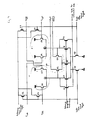
- FIG 4 is a schematic diagram of a preferred embodiment of a shared BiCMOS sense amplifier according to the present invention.
- the inputs to the circuit are V left and V left ⁇ , the left side memory cell block's true and complement output signals, and V right and V right ⁇ , the right side memory cell block's true and complement output signals.
- the sense amplifier also receives left and right side select input signals for selecting which group of memory cells will provide the input signal to the sense amplifier, a voltage reference signal for the unselected side's input buses, and a voltage reference signal for the MOS current sources.
- the outputs from the circuit of Figure 4 are the true output ("Output") and its complement (“ Output "), as well as a leakage path for the nonselected side.
- Sense amplifier 60 comprised of transistors 62 and 64, provides the OUTPUT and OUTPUT output signals. Depending upon which side of the memory array is selected, sense amplifier 60 receives its input from V left and V left ⁇ or V right or V right ⁇ . In turn, the initial selection of these input signals is controlled by two wired OR logic gates, 70 and 80, comprised respectively of transistors 57 and 58 and 56 and 59. V left and V right are the input signals to the bases of transistors 59 and 56, respectively, and V left ⁇ and V right ⁇ are the input signals to the bases of transistors 58 and 57, respectively. The emitters of transistors 58 and 57, as well as the emitters of transistors 59 and 56 are coupled together and connected to the bases of transistors 62 and 64, respectively.
- Transistors 67 and 71 act as current sources and are coupled to the output nodes of wired OR circuits 70 and 80, respectively.
- Current source 69 is coupled to the emitters of transistors 62 and 64.
- Transistors 75 and 77 act as switches and their gates are coupled to the left and right side select input signals, respectively, and their sources are coupled to the drains of current sources 67, 69, and 71.
- Transistors 67, 69, and 71 provide the current sources for differential sense amplifier 60 as well as for the transistors 56 through 59, which form the wired OR circuits 70 and 80.
- Transistor 69 provides roughly a milliamp of current while the emitter follower current sources (transistors 67 and 71) provide approximately 200 ⁇ A.
- Transistors 67, 69, and 71 have been chosen to act as ideal constant current sources rather than resistors to insure a steady current through the OR gates and sense amplifier even if the voltage across the transistors varies.
- Emitter follower nodes A and B are held low when the circuit is not being used through transistors 65 and 73 and the leakage path output.
- this circuit will be discussed using a left side select command as an example.
- the operation of the circuit is reversed when a right side select command is received.
- transistor 75 Upon receipt of a left side select signal, which is active high, transistor 75 is turned on and conducts current. In turn this permits current flow through current source transistors 67, 69, and 71.
- the same left side select signal also turns off transistors 52 and 54, which are PMOS transistors and inactive when their gates are high. When transistors 52 and 54 turn off, this disconnects the left side differential input lines V left and V left ⁇ from the reference voltage signal. Because the right side select signal is off (low), transistors 53 and 55 are on, bringing the unselected input lines V right and V right ⁇ to approximately V dd -0.4V, the reference voltage for unselected inputs. This voltage is a lower voltage than that appearing on the V left and V left ⁇ input lines.
- V left ⁇ and V left appear on the bases of transistors 58 and 59, which transistors respectively form one base of wired OR logic circuits 70 and 80.
- the reference voltage for unselected input lines appears on the bases of transistor 56 and 57, the other transistors in wired OR circuits 70 and 80.
- V left and V left ⁇ turn on transistors 59 and 58, respectively, with transistors 56 and 57 not conducting.
- V left and V left ⁇ now appear on the inputs to sense amplifier 60, the bases of transistors 62 and 64, after a single V BE drop across transistors 58 and 59.
- the differential between these signals then causes one of the two outputs Output or Output to go high indicating whether the sensed cell was a 1 or 0.
- the arrangement suggested herein for a single sense amplifier to detect the contents of both a right and left memory cell block also allows for the reduction of output parasitic capacitances by one-half. This follows naturally from the fact that only one amplifier is coupled to the output lines, instead of a separate right and left side sense amplifier, the two amplifiers each being coupled to a single output signal bus.
Landscapes
- Engineering & Computer Science (AREA)
- Microelectronics & Electronic Packaging (AREA)
- Computer Hardware Design (AREA)
- Static Random-Access Memory (AREA)
Applications Claiming Priority (2)
| Application Number | Priority Date | Filing Date | Title |
|---|---|---|---|
| US07/506,972 US5046050A (en) | 1990-04-10 | 1990-04-10 | Shared BiCMOS sense amplifier |
| US506972 | 1995-07-28 |
Publications (2)
| Publication Number | Publication Date |
|---|---|
| EP0451594A2 true EP0451594A2 (de) | 1991-10-16 |
| EP0451594A3 EP0451594A3 (de) | 1992-12-30 |
Family
ID=24016758
Family Applications (1)
| Application Number | Title | Priority Date | Filing Date |
|---|---|---|---|
| EP19910104704 Withdrawn EP0451594A3 (de) | 1990-04-10 | 1991-03-26 | Geteilter BICMOS-Leseverstärker |
Country Status (4)
| Country | Link |
|---|---|
| US (1) | US5046050A (de) |
| EP (1) | EP0451594A3 (de) |
| JP (1) | JPH04228190A (de) |
| KR (1) | KR100207941B1 (de) |
Cited By (1)
| Publication number | Priority date | Publication date | Assignee | Title |
|---|---|---|---|---|
| US8526256B2 (en) | 2011-09-16 | 2013-09-03 | International Business Machines Corporation | Single-ended sense amplifier with read-assist |
Families Citing this family (25)
| Publication number | Priority date | Publication date | Assignee | Title |
|---|---|---|---|---|
| JP2504571B2 (ja) * | 1989-08-04 | 1996-06-05 | 富士通株式会社 | 半導体集積回路装置 |
| KR100194743B1 (ko) * | 1989-09-14 | 1999-06-15 | 가나이 쓰도무 | 비교 기능을 갖는 반도체 메모리 장치 |
| JP2533399B2 (ja) * | 1990-05-25 | 1996-09-11 | 三菱電機株式会社 | センスアンプ |
| US5222045A (en) * | 1990-05-25 | 1993-06-22 | Mitsubishi Denki Kabushiki Kaisha | Semiconductor memory device operable with power supply voltage variation |
| US5287314A (en) * | 1992-05-26 | 1994-02-15 | Motorola, Inc. | BICMOS sense amplifier with reverse bias protection |
| US5568073A (en) * | 1993-12-22 | 1996-10-22 | Sgs-Thomson Microelectronics, Inc. | Data comparing sense amplifier |
| US5748554A (en) * | 1996-12-20 | 1998-05-05 | Rambus, Inc. | Memory and method for sensing sub-groups of memory elements |
| US6721860B2 (en) * | 1998-01-29 | 2004-04-13 | Micron Technology, Inc. | Method for bus capacitance reduction |
| US6349051B1 (en) | 1998-01-29 | 2002-02-19 | Micron Technology, Inc. | High speed data bus |
| US7269212B1 (en) | 2000-09-05 | 2007-09-11 | Rambus Inc. | Low-latency equalization in multi-level, multi-line communication systems |
| US7124221B1 (en) | 1999-10-19 | 2006-10-17 | Rambus Inc. | Low latency multi-level communication interface |
| US7161513B2 (en) | 1999-10-19 | 2007-01-09 | Rambus Inc. | Apparatus and method for improving resolution of a current mode driver |
| US6396329B1 (en) | 1999-10-19 | 2002-05-28 | Rambus, Inc | Method and apparatus for receiving high speed signals with low latency |
| US7500075B1 (en) | 2001-04-17 | 2009-03-03 | Rambus Inc. | Mechanism for enabling full data bus utilization without increasing data granularity |
| US6825841B2 (en) * | 2001-09-07 | 2004-11-30 | Rambus Inc. | Granularity memory column access |
| DE10145556C2 (de) * | 2001-09-14 | 2003-10-30 | Infineon Technologies Ag | Bewerter für Halbleiterspeicher |
| US6771536B2 (en) | 2002-02-27 | 2004-08-03 | Sandisk Corporation | Operating techniques for reducing program and read disturbs of a non-volatile memory |
| US7292629B2 (en) * | 2002-07-12 | 2007-11-06 | Rambus Inc. | Selectable-tap equalizer |
| US8861667B1 (en) | 2002-07-12 | 2014-10-14 | Rambus Inc. | Clock data recovery circuit with equalizer clock calibration |
| US7362800B1 (en) | 2002-07-12 | 2008-04-22 | Rambus Inc. | Auto-configured equalizer |
| US8190808B2 (en) * | 2004-08-17 | 2012-05-29 | Rambus Inc. | Memory device having staggered memory operations |
| US7280428B2 (en) | 2004-09-30 | 2007-10-09 | Rambus Inc. | Multi-column addressing mode memory system including an integrated circuit memory device |
| US8595459B2 (en) | 2004-11-29 | 2013-11-26 | Rambus Inc. | Micro-threaded memory |
| US20070260841A1 (en) | 2006-05-02 | 2007-11-08 | Hampel Craig E | Memory module with reduced access granularity |
| US9268719B2 (en) | 2011-08-05 | 2016-02-23 | Rambus Inc. | Memory signal buffers and modules supporting variable access granularity |
Family Cites Families (3)
| Publication number | Priority date | Publication date | Assignee | Title |
|---|---|---|---|---|
| US4351034A (en) * | 1980-10-10 | 1982-09-21 | Inmos Corporation | Folded bit line-shared sense amplifiers |
| JPS59104791A (ja) * | 1982-12-04 | 1984-06-16 | Fujitsu Ltd | 半導体記憶装置 |
| US4785259A (en) * | 1988-02-01 | 1988-11-15 | Motorola, Inc. | BIMOS memory sense amplifier system |
-
1990
- 1990-04-10 US US07/506,972 patent/US5046050A/en not_active Expired - Lifetime
-
1991
- 1991-03-26 EP EP19910104704 patent/EP0451594A3/de not_active Withdrawn
- 1991-04-09 KR KR1019910005626A patent/KR100207941B1/ko not_active Expired - Fee Related
- 1991-04-10 JP JP3164050A patent/JPH04228190A/ja active Pending
Cited By (1)
| Publication number | Priority date | Publication date | Assignee | Title |
|---|---|---|---|---|
| US8526256B2 (en) | 2011-09-16 | 2013-09-03 | International Business Machines Corporation | Single-ended sense amplifier with read-assist |
Also Published As
| Publication number | Publication date |
|---|---|
| US5046050A (en) | 1991-09-03 |
| KR100207941B1 (ko) | 1999-07-15 |
| EP0451594A3 (de) | 1992-12-30 |
| JPH04228190A (ja) | 1992-08-18 |
| KR910019051A (ko) | 1991-11-30 |
Similar Documents
| Publication | Publication Date | Title |
|---|---|---|
| US5046050A (en) | Shared BiCMOS sense amplifier | |
| KR920007440B1 (ko) | 반도체 기억장치 및 액세스방법 | |
| US4862421A (en) | Sensing and decoding scheme for a BiCMOS read/write memory | |
| US4817057A (en) | Semiconductor memory device having improved precharge scheme | |
| KR910009442B1 (ko) | 반도체 기억장치 | |
| US6819600B2 (en) | Semiconductor memory device with offset-compensated sensing scheme | |
| JP3961024B2 (ja) | オフセット自動無効化を行うセンス増幅器 | |
| JP2685357B2 (ja) | 半導体記憶装置 | |
| US5418749A (en) | Semiconductor memory device | |
| US5068830A (en) | High speed static ram sensing system | |
| US5323345A (en) | Semiconductor memory device having read/write circuitry | |
| US4598389A (en) | Single-ended CMOS sense amplifier | |
| US7286425B2 (en) | System and method for capacitive mis-match bit-line sensing | |
| US5642314A (en) | Semiconductor integrated circuit | |
| EP0503524B1 (de) | Halbleiterspeicheranordnung | |
| US4380055A (en) | Static RAM memory cell | |
| JPH04271086A (ja) | 半導体集積回路 | |
| EP0594346A2 (de) | Verbesserter Abtastverstärker | |
| US5220532A (en) | Self-locking load structure for static ram | |
| JP2892697B2 (ja) | 半導体記憶装置 | |
| EP0350860B1 (de) | Halbleiterspeicher mit verbesserten Abfühlverstärkern | |
| JPH0689577A (ja) | 半導体記憶装置 | |
| JPH0787035B2 (ja) | 半導体記億装置 | |
| KR100246990B1 (ko) | 디램 | |
| JP2840068B2 (ja) | ダイナミック型ram |
Legal Events
| Date | Code | Title | Description |
|---|---|---|---|
| PUAI | Public reference made under article 153(3) epc to a published international application that has entered the european phase |
Free format text: ORIGINAL CODE: 0009012 |
|
| AK | Designated contracting states |
Kind code of ref document: A2 Designated state(s): DE FR GB IT |
|
| PUAL | Search report despatched |
Free format text: ORIGINAL CODE: 0009013 |
|
| AK | Designated contracting states |
Kind code of ref document: A3 Designated state(s): DE FR GB IT |
|
| 17P | Request for examination filed |
Effective date: 19930510 |
|
| 17Q | First examination report despatched |
Effective date: 19941201 |
|
| STAA | Information on the status of an ep patent application or granted ep patent |
Free format text: STATUS: THE APPLICATION IS DEEMED TO BE WITHDRAWN |
|
| 18D | Application deemed to be withdrawn |
Effective date: 19950726 |