EP0452801A2 - Dispositif semi-conducteur ayant un élément récepteur de lumière et sa méthode de fabrication - Google Patents
Dispositif semi-conducteur ayant un élément récepteur de lumière et sa méthode de fabrication Download PDFInfo
- Publication number
- EP0452801A2 EP0452801A2 EP91105732A EP91105732A EP0452801A2 EP 0452801 A2 EP0452801 A2 EP 0452801A2 EP 91105732 A EP91105732 A EP 91105732A EP 91105732 A EP91105732 A EP 91105732A EP 0452801 A2 EP0452801 A2 EP 0452801A2
- Authority
- EP
- European Patent Office
- Prior art keywords
- layer
- semiconductor
- semiconductor device
- region
- electrode
- Prior art date
- Legal status (The legal status is an assumption and is not a legal conclusion. Google has not performed a legal analysis and makes no representation as to the accuracy of the status listed.)
- Granted
Links
Images


Classifications
-
- H—ELECTRICITY
- H10—SEMICONDUCTOR DEVICES; ELECTRIC SOLID-STATE DEVICES NOT OTHERWISE PROVIDED FOR
- H10F—INORGANIC SEMICONDUCTOR DEVICES SENSITIVE TO INFRARED RADIATION, LIGHT, ELECTROMAGNETIC RADIATION OF SHORTER WAVELENGTH OR CORPUSCULAR RADIATION
- H10F30/00—Individual radiation-sensitive semiconductor devices in which radiation controls the flow of current through the devices, e.g. photodetectors
- H10F30/20—Individual radiation-sensitive semiconductor devices in which radiation controls the flow of current through the devices, e.g. photodetectors the devices having potential barriers, e.g. phototransistors
- H10F30/21—Individual radiation-sensitive semiconductor devices in which radiation controls the flow of current through the devices, e.g. photodetectors the devices having potential barriers, e.g. phototransistors the devices being sensitive to infrared, visible or ultraviolet radiation
- H10F30/22—Individual radiation-sensitive semiconductor devices in which radiation controls the flow of current through the devices, e.g. photodetectors the devices having potential barriers, e.g. phototransistors the devices being sensitive to infrared, visible or ultraviolet radiation the devices having only one potential barrier, e.g. photodiodes
- H10F30/223—Individual radiation-sensitive semiconductor devices in which radiation controls the flow of current through the devices, e.g. photodetectors the devices having potential barriers, e.g. phototransistors the devices being sensitive to infrared, visible or ultraviolet radiation the devices having only one potential barrier, e.g. photodiodes the potential barrier being a PIN barrier
-
- H—ELECTRICITY
- H10—SEMICONDUCTOR DEVICES; ELECTRIC SOLID-STATE DEVICES NOT OTHERWISE PROVIDED FOR
- H10F—INORGANIC SEMICONDUCTOR DEVICES SENSITIVE TO INFRARED RADIATION, LIGHT, ELECTROMAGNETIC RADIATION OF SHORTER WAVELENGTH OR CORPUSCULAR RADIATION
- H10F39/00—Integrated devices, or assemblies of multiple devices, comprising at least one element covered by group H10F30/00, e.g. radiation detectors comprising photodiode arrays
- H10F39/10—Integrated devices
- H10F39/103—Integrated devices the at least one element covered by H10F30/00 having potential barriers, e.g. integrated devices comprising photodiodes or phototransistors
-
- H—ELECTRICITY
- H10—SEMICONDUCTOR DEVICES; ELECTRIC SOLID-STATE DEVICES NOT OTHERWISE PROVIDED FOR
- H10F—INORGANIC SEMICONDUCTOR DEVICES SENSITIVE TO INFRARED RADIATION, LIGHT, ELECTROMAGNETIC RADIATION OF SHORTER WAVELENGTH OR CORPUSCULAR RADIATION
- H10F77/00—Constructional details of devices covered by this subclass
- H10F77/40—Optical elements or arrangements
- H10F77/407—Optical elements or arrangements indirectly associated with the devices
Definitions
- the present invention generally relates to semiconductor devices and methods of producing the same, and more particularly to a semiconductor device having pin photodiodes and a method of producing such a semiconductor device.
- the diameter of the pin junction is reduced and the thickness of an i-type photoabsorption semiconductor layer is reduced.
- the diameter of the pin junction becomes 20 ⁇ m or less and the thickness of the i-type photoabsorption semiconductor layer becomes 1 ⁇ m or less.
- a pin photodiode having a pin junction diameter of 15 ⁇ m and a photoabsorption layer with a thickness of 1.4 ⁇ m for subjecting an ultra high speed optical signal of 20 GHz or greater it is possible to realize a capacitance of 30 to 40 fP. But such a small photodiode easily breaks when affected by a surge voltage or the like.
- pin photodiode which is provided with a chip capacitor.
- the chip capacitor is provided adjacent to the pin photodiode chip and acts as a bypass capacitor for bypassing the surge voltage.
- this limit prevents complete elimination of the above described problem. In other words, it is difficult to positively prevent breakdown of the pin photodiode by quickly responding to even an impulse external noise.
- the pin photodiode has an i-type region sandwiched between a p-type region and an n-type region.
- An avalanche photodiode (APD) has an i-type region in which an avalanche breakdown occurs.
- the i-type region functions as a photoabsorption layer which absorbs light, and the material used for the photoabsorption layer changes depending on the wavelength of the light used for the optical communication.
- a description will now be made of the conventional light receiving elements which are designed for the optical communication using a light having a wavelength of approximately 1 ⁇ m such as 1.3 ⁇ m and 1.6 ⁇ m.
- FIG.1A shows a conventional pin photodiode.
- an n+-type InP layer 552 is formed on a semiinsulative InP substrate 551.
- An undoped InGaAs layer 553 which forms an i-type region for absorbing light is formed on the n+-type InP layer 552.
- An n ⁇ -type InP region 554 is formed on the InGaAs layer 553.
- a p+-type region 555 is formed within the n ⁇ -type InP layer 554 by diffusing Zn, so as to form a pin structure.
- the n+-type InP layer 552 has a thickness of 2 ⁇ m
- the InGaAs layer 553 has a thickness of 1.7 ⁇ m
- the n ⁇ -type InP layer 554 has a thickness of approximately 1 ⁇ m which is doped with Si with an impurity concentration of 1 x 1015 cm ⁇ 3.
- the n ⁇ -type InP layer 554 and the InGaAs layer 553 are selectively etched to expose the surface of the n+-type InP layer 552.
- the InGaAs layer 53 When a predetermined reverse bias voltage is applied across the electrodes 557 and 558 of the pin photodiode shown in FIG.1A, the InGaAs layer 53 essentially becomes a depletion layer. The electric field within the depletion layer accelerates the electron-hole pairs which are generated by the incident light, thereby causing the holes to be collected at the p side electrode 558 and the electrons to be collected at the n side electrode 557.
- FIG.1B shows a conventional lateral pin photodiode.
- an undoped InP layer 661 which acts as a buffer layer is formed on the semiinsulative InP substrate 551.
- An undoped InGaAs layer 662 which acts as a photoabsorption layer is formed on the InP layer 661.
- An n ⁇ -type InP layer 663 is formed on the InGaAs layer 662. Zn is selectively diffused within the n ⁇ -type InP layer 663 so as to form a p-type region 664.
- the InP layer 661 and the InGaAs layer 662 are made of a substantially intrinsic semiconductor having an impurity concentration of 1 x 1014 cm ⁇ 3 or less.
- the InP layer 661 and the InGaAs layer 662 have thicknesses of approximately 1 ⁇ m and 1.7 ⁇ m, respectively.
- the n ⁇ -type InP layer 663 has a thickness of approximately 0.3 ⁇ m and an impurity concentration of approximately 1 x 1015 cm ⁇ 3.
- a p side electrode 668 which is made of AuZn/Au is formed on the p-type region 664, and an n side electrode 667 which is made of AuGe/Au is formed on the n ⁇ -type InP layer 663.
- FIG.1C shows a conventional metal-semiconductor-metal (MSM) photodiode.
- the InP layer 661 which acts as the buffer layer is formed on the semiinsulative InP substrate 551 and the InGaAs layer 662 which acts as the photoabsorption layer is formed on the InP layer 661, similarly to the lateral pin photodiode shown in FIG.1B.
- An undoped InAlAs layer 771 having a thickness of approximately 0.1 ⁇ m is formed on the InGaAs layer 662 for forming a Schottky contact.
- Schottky electrodes 772 and 773 which are made of Al or the like are formed directly on the InAlAs layer 771.
- the electrodes 772 and 773 have comb shapes which intermesh each other in the plan view.
- a negative voltage is applied to the electrode 772 and a positive voltage is applied to the electrode 773 as shown, an electric field indicated by arrows is generated from the electrode 773 towards the electrode 772, penetrating the InGaAs layer (photoabsorption layer) 662.
- the incident light reaches the InGaAs layer 662 and the electron-hole pairs are generated by the absorption of light, the electrons and holes are accelerated by the electric field and are respectively collected at the electrodes 773 and 772.
- a barrier is generated at a hetero interface between the InAlAs layer 771 which forms the Schottky barrier and the InGaAs layer 662 which forms the photoabsorption layer, thereby forming a carrier trap. Consequently, it is difficult to obtain a sufficiently high response speed unless the composition of the InAlAs layer 771 is controlled so that the composition at the interface between the InAlAs layer 771 and the InGaAs layer 662 is close to InGaAs. In addition, a region is generated where the electric field uneasily develops immediately under the electrode. When the carriers are generated in such a region, the response speed of the MSM photodiode becomes poor.
- Another and more specific object of the present invention is to provide a semiconductor device comprising a substrate, a first layer formed on the substrate and made of a semiconductor of a first conductive type, a second layer formed on the first layer and functioning as a photoabsorption layer, a third layer formed on the second layer and made of a semiconductor of the first conductive type, a plurality of regions formed in the third layer and made of a semiconductor of a second conductive type opposite to the first conductive type thereby forming a plurality of pin diodes, where each of the regions at least reaches the second layer, and a plurality of electrodes respectively formed on the regions and made of the same electrode material, where a first electrode out of the electrodes receives a positive voltage to forward bias a first pin diode out of the pin diodes and a second electrode out of the electrodes receives a negative voltage to reverse bias a second pin diode out of the pin diodes so that the second pin diode operates as a pin photodiode.
- the electrodes can be formed substantially on the same plane and the semiconductor device can easily be mounted on a part by the so-called flip-chip bonding.
- Still another object of the present invention is to provide a semiconductor device comprising a substrate, a first layer formed on the substrate and made of a semiconductor, a second layer formed on the first layer and made of a semiconductor of a first conductive type with a first band gap, a third layer formed on the second layer and made of a material having a second band gap which is smaller than the first band gap, the third layer functioning as a photoabsorption layer, a fourth layer formed on the third layer and made of a semiconductor of the first conductive type with an impurity concentration greater than that of the third layer, a plurality of regions formed in the fourth layer and made of a semiconductor of a second conductive type opposite to the first conductive type thereby forming a plurality of pin diodes, each of the regions at least reaching the third layer, and a plurality of electrodes respectively formed on the regions and made of the same electrode material, where a first electrode out of the electrodes is connected to a first region out of the regions and receives a positive voltage to forward bias a first pin
- the electrodes can be formed substantially on the same plane and the semiconductor device can easily be mounted on a part by the so-called flip-chip bonding. In addition, it is possible to improve the utilization efficiency of the area occupied by the electrodes.
- a further object of the present invention is to provide a semiconductor device comprising a substrate, a first layer formed on the substrate and made of a semiconductor, a second layer formed on the first layer and made of a semiconductor of a first conductive type with a first band gap, a third layer formed on the second layer and made of a material having a second band gap which is smaller than the first band gap, where the third layer functions as a photoabsorption layer, a fourth layer formed on the third layer and made of a semiconductor of the first conductive type with an impurity concentration greater than that of the third layer, and a plurality of Schottky electrodes respectively formed on the fourth layer in a plurality of regions and made of the same electrode material, where a first electrode out of the electrodes is connected to a first region out of the regions of the fourth layer and receives a positive voltage to forward bias a first pin diode out of the pin diodes, the first region has a first area of contact with the fourth layer, a second electrode out of the electrodes is connected to
- the electrodes can be formed substantially on the same plane and the semiconductor device can easily be mounted on a part by the so-called flip-chip bonding. In addition, it is possible to improve the utilization efficiency of the area occupied by the electrodes.
- Another object of the present invention is to provide a semiconductor device comprising a semiinsulative substrate, a first stacked structure formed on the semiinsulative substrate and including layers for forming an electronic element, and a second stacked structure formed on the first stacked structure and including layers for forming an optoelectronic element, where the second stacked structure includes a first layer formed on the first stacked structure and made of a semiconductor of a first conductive type with a first band gap, a second layer formed on the first layer and made of a material having a second band gap which is smaller than the first band gap, where the second layer functions as a photoabsorption layer, a third layer formed on the second layer and made of a semiconductor of the first conductive type with an impurity concentration greater than that of the second layer, a plurality of regions formed in the third layer and made of a semiconductor of a second conductive type opposite to the first conductive type thereby forming a plurality of pin diodes, where each of the regions at least reach the second layer, and a plurality of
- a first electrode out of the electrodes is connected to a first region out of the regions and receives a positive voltage to forward bias a first pin diode out of the pin diodes, the first region has a first area of contact with the third layer, a second electrode out of the electrodes is connected to a second region out of the regions and receives a negative voltage to reverse bias a second pin diode out of the pin diodes, the second region has a second area of contact with the third layer, and the second area is larger than the first area.
- Still another object of the present invention is to provide a semiconductor device comprising a semiinsulative substrate, a first stacked structure formed on the semiinsulative substrate and including layers for forming an electronic element, and a second stacked structure formed on the first stacked structure and including layers for forming an optoelectronic element, where the second stacked structure includes a first layer formed on the first stacked structure and made of a semiconductor of a first conductive type with a first band gap, a second layer formed on the first layer and made of a material having a second band gap which is smaller than the first band gap, where the second layer functions as a photoabsorption layer, a third layer formed on the second layer and made of a semiconductor of the first conductive type with an impurity concentration greater than that of the second layer, and a plurality of Schottky electrodes respectively formed on the third layer in a plurality of regions and made of the same electrode material.
- a first electrode out of the electrodes is connected to a first region out of the regions of the third layer and receives a positive voltage to forward bias a first pin diode out of the pin diodes, the first region has a first area of contact with the third layer, a second electrode out of the electrodes is connected to a second region out of the regions of the third layer and receives a negative voltage to reverse bias a second pin diode out of the pin diodes, the second region has a second area of contact with the third layer, and the second area is larger than the first area.
- a further object of the present invention is to provide a method of producing a semiconductor device comprising the steps of successively forming first, second and third layers on a substrate, where the first layer is made of a semiconductor of a first conductive type, the second layer functions as a photoabsorption layer and the third layer is made of a semiconductor of the first conductive type, forming a mask layer on the third layer, forming a plurality of openings in the mask layer by an etching, implanting impurities into the third layer via the openings of the mask layer to form a plurality of regions made of a semiconductor of a second conductive type opposite to the first conductive type thereby forming a plurality of pin diodes, where each of the regions at least reach the second layer, removing the mask layer, and forming a plurality of electrodes respectively on the regions, where the electrodes are made of the same electrode material.
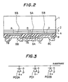
- FIG.2 shows a cross section of an essential part of the semiconductor device
- FIG.3 shows an equivalent circuit of the first embodiment when the necessary connections are made.
- the semiconductor device shown in FIG.2 includes a semiconductor substrate 1, an n-type semiconductor layer 2, an i-type photoabsorption layer 3, an n-type semiconductor (semiinsulative) layer 4, p-type window regions 5A and 5B, an insulating layer 9 made of polyimide, for example, electrodes 7A, 7B and 7C for taking out the photocurrent, and electrodes 8A, 8B and 8C for making the necessary connections.
- Pin photodiodes PD1, PD2A and PD2B shown in FIG.3 are formed by making the necessary connections.
- the pin photodiode PD1 is made up of the n-type semiconductor layer 2, the i-type photoabsorption layer 3, the p-type window region 5A and the like. As may be seen from the p-type window region 5A, the pin photodiode PD1 has an extremely small pin junction area. On the other hand, the pin photodiodes PD2A and PD2B have considerably large pin junction areas compared to that of the pin photodiode PD1.
- a bias voltage is applied to the pin photodiodes PD1, PD2A and PD2B with the polarity shown in FIG.3.
- the bias voltage is applied so that the polarity of the electrode 8A becomes negative and the polarity of the electrode 8B becomes positive.
- a reverse bias voltage is applied to the pin photodiode PD1, and the pin photodiode PD1 operates as a pin photodiode.
- a forward bias voltage is applied to each of the pin photodiodes PD2A and PD2B, and the pin photodiodes PD2A and PD2B do not operate as pin photodiodes.
- the electrostatic capacitances of the pin photodiodes PD2A and PD2B are large because of the considerably large pin junction areas, and the pin photodiodes PD2A and PD2B are essentially short-circuits with respect to a high-frequency electrical signal.
- the semiconductor substrate 1 is made of n+-type InP
- the n-type semiconductor layer 2 is made of n+-type InP
- the i-type photoabsorption layer 3 is made of undoped InGaAs
- the n-type semiconductor layer 4 is made of n ⁇ -type InP.
- the pin photodiodes PD2A and PD2B other than the pin photodiode PD1 which carries out the photoelectric conversion occupy relatively large areas and can provide stable support when mounting the semiconductor device.
- the forward bias voltage is applied to the pin photodiodes PD2A and PD2B, a large photocurrent can be obtained from these pin photodiodes PD2A and PD2B without problems.
- the structure in this embodiment is particularly suited for the so-called flip-chip bonding, and it is thus possible to minimize the stray inductance and stray capacitance and to prevent characteristic deterioration of the semiconductor device.
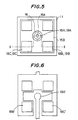
- FIG.5 shows a plan view of an essential part of the first embodiment
- FIG.4 shows a cross section taken along a line X-X in FIG.5.
- the semiconductor device shown in FIGS.4 and 5 includes an n+-type InP substrate 11 which includes a micro lens 11A.
- An n+-type InP layer 12, an undoped InGaAs photoabsorption layer 13, and an n ⁇ -type InP layer 14 are successively stacked on the n+-type InP substrate 11.
- a p-type window region 15A and p-type widow regions 15B are formed in the n ⁇ -type InP layer 14.
- An insulator layer 21 made of polyimide is formed on the n ⁇ -type InP layer 14. Electrodes are formed on the p-type window regions 15A and 15B.
- One electrode which connects to the p-type window region 15A is made up of an ohmic contact metal layer 17, a barrier metal electrode 18A and a connecting electrode 19A.
- Each electrode which connects to the p-type window region 15B is made up of an ohmic contact metal layer 17, a barrier metal electrode 18B or 18C, and a connecting electrode 19B or 19C.
- a non-reflecting coating layer 20 is formed on the surface of the n+-type InP substrate 11.
- the thickness, impurity concentration and the like of the layers forming the fourth embodiment are selected as follows, for example.
- the n+-type InP substrate 11 has a thickness S1 of 70 ⁇ m and an impurity concentration of 1 x 1018 cm ⁇ 3.
- the micro lens 11A has a maximum thickness S2 of 6 ⁇ m and an aperture diameter of 50 ⁇ m.
- the n+-type InP layer 12 has a thickness of 1.5 ⁇ m and an impurity concentration of 1 x 1018 cm ⁇ 3.
- the InGaAs photoabsorption layer 13 has a thickness of 1.4 ⁇ m.
- the n ⁇ -type InP layer 14 has a thickness of 1 ⁇ m and an impurity concentration of 1 x 1016 cm ⁇ 3.
- the p-type window regions 15A and 15B are doped with Zn as the impurity and have an impurity concentration of approximately 1 x 1018 cm ⁇ 3.
- the insulator layer 21 has a thickness of 2 ⁇ m.
- the ohmic contact metal layer 17 is made up of a AuZn/Au structure.
- the barrier metal electrodes 18A, 18B and 18C are respectively made up of a Ti/Pt/Au structure.
- the connecting electrodes 19A, 19B and 19C are respectively made of AuSn.
- the diameter of the pin junction of the pin photodiode which includes the p-type window region 15A is in the range of 5 to 10 ⁇ m and extremely small.
- the back surface of the substrate 11 is formed as the micro lens 11A having the aperture diameter of 50 ⁇ m so as to converge the incident light which is to reach the p-type window region 15A.
- the pin junction below the micro lens 11A is extremely small, no stepped portion exists at the top surface of the semiconductor device.
- the electrodes 18A and 19A for use in taking out the photocurrent can be formed to the approximately inverted T-shape which is relatively large, and it is possible to prevent increase of the stray capacitance as described above.
- FIG.6 shows a plan view of an essential part of a pattern to which the first embodiment is to be mounted.
- parts 19A', 19B' and 19C' respectively indicate positions where the corresponding electrodes 19A, 19B and 19C are bonded.
- the bonding of the semiconductor device shown in FIG.5 onto the pattern shown in FIG.6 is made by the so-called flip-chip bonding.
- the number of connecting electrodes and the arrangement thereof are not limited to those of the fourth embodiment shown in FIG.5.
- the connecting electrodes may have different sizes, and the position of the pin photodiode which actually carries out the photoelectric conversion is not limited to the center of the semiconductor device.
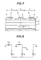
- a substrate 1 is made of a semiinsulative or conductive semiconductor such as InP and GaAs.
- an n+-type semiconductor substrate is used as the substrate 1.
- An n+-type semiconductor layer 2 which is made of n+-type InP, n+-type AlGaAs or the like is formed on the n+-type substrate 1.
- a photoabsorption layer 3 which is made of undoped InGaAs, undoped GaAs or the like is formed on the n+-type semiconductor layer 2.
- An n ⁇ -type window layer 4 which is made of n ⁇ -type InP, n ⁇ -type AlGaAs or the like is formed on the photoabsorption layer 3.
- a plurality of p-type window regions 5 are formed in the n ⁇ -type window layer 4, and an electrode for connection is formed on each p-type window region 5.
- A, B and C denote pin photodiode parts.
- the pin photodiode parts A and C are large compared to the pin photodiode part B.
- the pin junction area at the pin photodiode parts A and C is large compared to that at the pin photodiode part B.
- FIG.8 shows an equivalent circuit of the semiconductor device shown in FIG.7 when the necessary connections are made to operate the semiconductor device.
- the same designations are used as in FIG.7.
- the pin photodiode part A is connected in a forward direction with respect to a power source PS and acts as a power supply.
- the pin photodiode part B is applied with a reverse bias voltage and acts as a photodiode itself.
- the pin photodiode part C is connected in a reverse direction with respect to the power source PS.
- the pin photodiode part C acts as a bypass capacitor for bypassing the surge voltage when the surge voltage is applied to the pin photodiode part B which is extremely small.
- FIG.9 shows a plan view of an essential part of the second embodiment.
- FIGS.10 and 11 respectively are cross sectional views taken along lines X1-X1 and X2-X2 in FIG.9.
- an n+-type InP substrate 11 includes S as the impurity and the impurity concentration is 2 x 1018 cm ⁇ 3.
- An n+-type InP layer 12 having a thickness of 1.0 ⁇ m includes Si as the impurity and the impurity concentration is 5 x 1017 cm ⁇ 3.
- An undoped InGaAs photoabsorption layer 13 has a thickness of 1.4 ⁇ m.
- An n ⁇ -type InP window layer 14 having a thickness of 1 ⁇ m includes Si as the impurity and the impurity concentration is 1 x 1016 cm ⁇ 3.
- a p-type window region 15 includes Zn as the impurity and the impurity concentration is 1 x 1018 cm ⁇ 3.
- An electrode 16 uses a contact metal made of a Au/Zn/Au structure, a barrier metal made of a Ti/Pt structure, an electrode draw-out metal made of Au, and a flip-chip bonding material made of Ausn.
- the thickness of the contact metal is 400 ⁇ /80 ⁇ /120 ⁇ , and the thickness of the barrier metal is 500 ⁇ /3000 ⁇ .
- the thickness of the electrode draw-out metal is 2000 ⁇ , and the thickness of the flip-chip bonding material is 3 ⁇ m.
- FIGS.12 and 13 those parts which are the same as those corresponding parts in FIGS.7 and 8 are designated by the same reference numerals, and a description thereof will be omitted.
- FIG.12 which shows a cross section of the semiconductor device, a p-type window region 5' is provided in a pn junction diode part A'.
- This window region 5' may be made of an n-type semiconductor.
- the pin photodiode part A shown in FIG.7 acts only as an interconnection device for supplying negative voltage to part B.
- the i-type photoabsorption layer 3 is unnecessary for the operation of the pin photodiode part A, and the existence of the i-type photoabsorption layer 3 rather generates a forward voltage drop.
- the p-type window region 5' is made deep to reach the n+-type semiconductor layer 2.
- FIG.13 shows an equivalent circuit of the semiconductor device shown in FIG.12 when the necessary connections are made to operate the semiconductor device.
- the equivalent circuit shown in FIG.13 differs from that shown in FIG.8 in that the pn junction diode part A' is provided in place of the pin photodiode part A.
- the pn junction diode part A' is completely short-circuited as indicated by a broken line in FIG.13.
- FIG.14 those parts which are the same as those corresponding parts in FIGS.9 through 11 are designated by the same reference numerals, and a description thereof will be omitted.
- FIG.14 corresponds to an essential part of the third embodiment along the line X2-X2 shown in FIG.9 when the structure shown in FIG.9 is employed.
- a depression 14A is formed in the n ⁇ -type InP window layer 14.
- the depression 14A is formed by etching the surface of the n ⁇ -type InP window layer 14.
- a deep p-type window region 25 is formed by an impurity diffusion which is carried out to form the p-type window regions 15 of the pin photodiode parts B and C.
- the p-type window regions 15 and 25 are formed simultaneously, although the p-type window region 25 is deeper than the p-type regions 15.
- FIG.15 shows a plan view of an essential part of the third embodiment.
- FIGS.16 and 17 respectively are cross sectional views taken along lines X1-X1 and X2-X2 in FIG.15.
- FIGS.15 through 17 those parts which are the same as those corresponding parts in FIGS.9 through 11 are designated by the same reference numerals, and a description thereof will be omitted.
- the n ⁇ -type InP window layer 14 and the InGaAs photoabsorption layer 12 have a mesa structure, unlike the first embodiment shown in FIGS.9 through 11.
- the p-type window region 15 of the pin photodiode part A reaches the n+-type InP layer 12 via a p-type impurity diffusion region 17.
- an n-type semiconductor may be used for the window region 15 of the pin photodiode part A. But in this case, it is preferable to connect the n-type window region 15 and the n+-type InP layer 12 by forming an AuGe/Au layer on the side surface of the mesa structure.
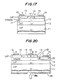
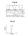
- FIG.18 shows a cross section of an essential part of the semiconductor device
- FIG.19 shows withstand voltages of the pin photodiode parts B and C in the reverse direction.
- those parts which are the same as those corresponding parts in FIGS.7, 8, 12 and 13 are designated by the same reference numerals, and a description thereof will be omitted.
- the pin photodiode part C includes a p-type window region 5''.
- the depth of this p-type window region 5'' is greater than the corresponding p-type window region 5 of the pin photodiode part C of the first embodiment shown in FIGS.9 through 11.
- the p-type window region 5'' of the pin photodiode part C which functions as a bypass capacitor is deeper than the p-type window regions 5 of the pin photodiode parts A and B.
- FIG.19 shows the withstand voltages of the pin photodiode parts B and C shown in FIG.18 in the reverse direction.
- the ordinate indicates the current and the abscissa indicates the voltage.
- the withstand voltage in the reverse direction at the pin junction of the pin photodiode part C which functions as the bypass capacitor is lower than the withstand voltage in the reverse direction at the pin junction of the pin photodiode part B which functions as a pin photodiode.
- the effect of protecting the pin photodiode part B from the surge voltage or the like is improved in this embodiment.
- the withstand voltage in the reverse direction drops in the pin photodiode part C because the interface of the p-type window region 5'' exists within the undoped InGaAs photoabsorption layer 3 which has a narrow energy band gap.
- the withstand voltage is high in the pin photodiode part B because the interface of the p-type window region 5 exists at the interface between the n ⁇ -type window layer 14 and the undoped InGaAs photoabsorption layer 13.
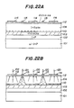
- FIG.20 corresponds to a cross section of the structure shown in FIG.9 taken along a diagonal direction.
- all of the electrodes 16 are shown in FIG.20 for the pin photodiode parts A, B and C.
- a depression 14B is formed in the n ⁇ -type InP window layer 14, and an n side electrode 28 is provided on the substrate 11.
- An opening 28A is formed in the n side electrode 28 for receiving the incoming light.
- the depression 14B is formed by etching the surface of the n ⁇ -type InP window layer 14.
- a deep p-type window region 35 is formed by an impurity diffusion which is carried out to form the p-type window regions 15 of the pin photodiode parts A and B.
- the p-type window regions 15 and 35 are formed simultaneously, although the p-type window region 35 is deeper than the p-type regions 15.
- the incident light is received via the opening 28A in the n side electrode 28 which is provided on the back or bottom surface of the substrate 11.
- the size of the rectangular chip is 200 ⁇ m x 200 ⁇ m.
- the diameter of the p-type window region 15 of the pin photodiode part B is 15 to 20 ⁇ m.
- the n+-type InP layer 12, the undoped InGaAs photoabsorption layer 13 and the n ⁇ -type InP window layer 14 are successively formed on the n+-type InP substrate by using metal organic vapor phase epitaxy (MOVPE) techniques.
- MOVPE metal organic vapor phase epitaxy
- a mask layer made of SiO2, SiN or the like is formed on the entire top surface of the structure by a thermal chemical vapor deposition (CVD), a plasma CVD or the like.
- CVD thermal chemical vapor deposition
- plasma CVD plasma CVD
- openings for implanting impurities are formed in the mask layer by an etching using a photolithography technique.
- the p-type window regions 15 are formed by implanting Zn via the openings in the mask layer using a thermal diffusion technique. For example, this thermal diffusion is carried out at a temperature of 500°C for approximately 30 minutes.
- the electrodes 16 are then formed using the resist process, vacuum deposition process and lift-off process of the photolithography technique. In other words, the mask layer is removed and the electrodes 16 are formed thereafter.
- the depression 14A or 14B can be formed in the n ⁇ -type InP layer 14 prior to forming the mask layer.
- the p side electrode of the pin photodiode part B which originally functions as the pin photodiode is connected to a load resistor R for converting the photocurrent into the voltage.
- the reverse bias voltage of the pin photodiode part B is constantly maintained to a small value.
- the pulse surge voltage in the pulse form is applied to the pin photodiode parts B and C, the pulse surge voltage is sufficiently absorbed by the large junction capacitance of the pin photodiode part C to prevent breakdown of the pin photodiode part B.
- FIGS.21A and 21B Next, a description will be given of a fifth embodiment of the semiconductor device according to the present invention, by referring to FIGS.21A and 21B.
- a semiinsulative InP substrate 101 is doped with Fe, and an undoped InP layer 102 is formed on the semiinsulative InP substrate 101 as a buffer layer.
- An n+-type InAlAs layer 103 having a wide band gap and a high impurity concentration is formed on the undoped InP layer 102 as a carrier supply layer.
- the n+-type InAlAs layer 103 has a thickness of approximately 1000 ⁇ and is doped with Si so that the impurity concentration is approximately 1 x 1018 cm ⁇ 3.
- An undoped InGaAs photoabsorption layer 104 having a relatively narrow band gap is formed on the n+-type InAlAs layer 103.
- the undoped InGaAs photoabsorption layer 104 has a thickness of approximately 1.7 ⁇ m.
- the undoped InGaAs photoabsorption layer 104 has a narrower band gap compared to that of the n+-type InAlAs layer 103 and receives the carriers (electrons) from the n+-type InAlAs layer 103.
- a two-dimensional carrier (electron) gas layer 110 is formed in a vicinity of an interface between the undoped InGaAs photoabsorption layer 104 and the n+-type InAlAs layer 103.
- n ⁇ -type InP window layer 105 having a wide band gap is formed on the undoped InGaAs photoabsorption layer 104.
- the n ⁇ -type InP window layer 105 has a thickness of approximately 0.3 ⁇ m and is doped with Si so that the impurity concentration is approximately 1 x 1016 cm ⁇ 3.
- Zn is selectively diffused into the n ⁇ -type InP window layer 105 to form p+-type InP regions 106 and 107.
- the p+-type InP region 106 is wider (or larger in area) than the p+-type InP region 107.
- Ohmic electrodes made up of a AuZn/Au structure is formed on each of the p+-type InP regions 106 and 107.
- a wide electrode 108 is formed on the wide p+-type InP region 106, and a narrow electrode 109 is formed on the narrow p+-type InP region 107.
- a reverse bias voltage (negative voltage) from a bias source 120 is applied to the wide electrode 108, while a forward bias voltage (positive voltage) from the bias source 120 is applied to the narrow electrode 109.
- FIG.21B shows the operating mechanism of the fifth embodiment shown in FIG.21A.
- a wide depletion layer is formed by the reverse bias under the wide electrode 108 which is applied with the negative voltage, that is, under the p+-type InP region 106. For this reason, the two-dimensional carrier gas layer 110 is pushed towards the boundary between the undoped InGaAs photoabsorption layer 104 and the n+-type InAlAs layer 103.
- the wide depletion layer with the approximately vertical interface is formed under the wide electrode 108 which is reverse biased.
- the electron-hole pairs are generated upon receipt of the incident light, these carriers are moved at a high speed due to the electric field.
- the two-dimensional carrier gas layer 110 is attracted towards the p+-type InP region 107 under the narrow electrode 109 which is forward biased. For this reason, the electrode 109 and the two-dimensional carrier gas layer 110 are connected via a low resistance, and the two-dimensional carrier gas layer 110 acts as an intermediate electrode.
- the electric field develops vertically in a wide region within the undoped InGaAs photoabsorption layer 104, thereby forming a high-speed response region.
- the two-dimensional carrier gas layer 110 is satisfactorily conductive, it is possible to eliminate a region in which the carrier transport is slow when the light is absorbed. As a result, the response speed of the photodiode becomes high.
- the positive and negative electrodes 108 and 109 are connected to the p+-type InP regions 106 and 107 using an ohmic contact.
- FIGS.22A and 22B a description will be given of a sixth embodiment of the semiconductor device according to the present invention, by referring to FIGS.22A and 22B.
- the concept of the fifth embodiment is applied to the MSM photodiode which employs the Schottky contact.
- FIGS.22A and 22B those parts which are the same as those corresponding parts in FIGS.21A and 21B are designated by the same reference numerals, and a description thereof will be omitted.
- an n ⁇ -type InAlAs Schottky contact layer 112 for forming a Schottky contact is formed on the undoped InGaAs photoabsorption layer 104.
- the n ⁇ -type InAlAs Schottky contact layer 112 has a thickness of approximately 200 ⁇ .
- a wide Schottky contact electrode 114 having a large area and a narrow Schottky contact electrode 115 having a small area are respectively made of Al and are formed on the n ⁇ -type InAlAs Schottky contact layer 112.
- the n+-type InAlAs layer (carrier supply layer) 103 has a thickness of approximately 1000 ⁇ and is doped with Si so that the impurity concentration is approximately 1 x 1018 cm ⁇ 3.
- the undoped InGaAs photoabsorption layer 104 has a thickness of approximately 1.7 ⁇ m
- the n ⁇ -type InAlAs Schottky contact layer 112 has a thickness of approximately 200 ⁇ .
- the carriers are supplied from the n+-type InAlAs layer (carrier supply layer) 103 to the undoped InGaAs photoabsorption layer 104, similarly as in the case of the fifth embodiment, and the two-dimensional carrier gas layer 110 is formed in the vicinity of the interface between the n+-type InAlAs layer 103 and the undoped InGaAs photoabsorption layer 104.
- the two-dimensional carrier gas layer 110 has a low resistance, and confronts the Schottky electrode 114 and 115 via the undoped InGaAs photoabsorption layer 104.
- FIG.22B shows the operating mechanism of the sixth embodiment shown in FIG.22A.
- a negative voltage for reverse biasing is applied to the wide Schottky electrode 114, and a positive voltage for forward biasing is applied to the narrow Schottky electrode 115.
- the two-dimensional carrier gas layer 110 is pulled upwardly by the positive voltage applied to the Schottky electrode 115 and is distributed close to the Schottky electrode 115.
- the two-dimensional carrier gas layer 110 is pushed downwardly by the negative voltage applied to the Schottky electrode 114, towards the boundary between the undoped InGaAs photoabsorption layer 104 and the n+-type InAlAs layer 103, thereby forming a wide depletion layer.
- the undoped InGaAs photoabsorption layer 104 is occupied by the depletion layer and the low resistance region. Therefore, when the incident light is absorbed by the undoped InGaAs photoabsorption layer 104 and the electron-hole pairs are generated, these carriers are quickly drawn towards the Schottky electrode 114 and 115.
- the carrier supply layer 103 is made of InAlAs.
- any material such as InP which has a wide band gap and forms a lattice matching with the photoabsorption layer 104 may be used for the carrier supply layer 103.
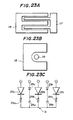
- FIG.23A shows a plan view of a pattern of the electrodes 108 and 109 or the electrodes 114 and 115 when the interdigital type electrodes are used.
- a comb shaped electrode 116 having a relatively large area and a comb shaped electrode 117 having a relatively small area confront each other in an intermeshing manner to form the interdigital type electrodes.
- a reverse bias voltage is applied to the electrode 116 and a forward bias voltage is applied to the electrode 117, a depletion layer is widely formed under the electrode 116 and a light sensitive region is generated.
- FIG.23B shows a plan view of a pattern of the electrodes 108 and 109 or the electrodes 114 and 115 when a peripheral electrode surrounds a center electrode.
- an electrode 118 having a relatively large area surrounds an electrode 119 having a relatively small area.
- the part of the electrode 119 becomes the light receiving region.
- a forward bias voltage is applied to the electrode 118 and a reverse bias voltage is applied to the electrode 119.
- the part of the electrode 118 becomes the light receiving region.
- the light receiving region changes similarly for the interdigital type electrodes shown in FIG.23A.
- FIG.23C shows an equivalent circuit of photodiodes which use electrodes having different areas.
- FIG.23C shows the equivalent circuit for the case shown in FIG.23A where there are three electrodes having the relatively large area and two electrodes having the relatively small area.
- Diodes 122a, 122b and 122c having the relatively large areas and diodes 123a and 123b having the relatively small areas are coupled in parallel as shown in FIG.23C.
- the diodes 122a, 122b, 122c, 123a and 123b respectively have internal resistances 124a, 124b, 124c, 125a and 125b.
- the two-dimensional carrier gas layer is drawn towards the electrode and the internal resistances 125a and 125b thereof are small.
- the two-dimensional carrier gas layer is pushed away from the electrode when a reverse bias voltage is applied to each of the diodes 122a, 122b and 122c, and the internal resistances 124a, 124b and 124c thereof are large.
- the diodes 123a and 123b which are applied with the forward bias voltage and the resistances 125a and 125b substantially act as electrodes which connected to a common node N.
- the diodes 122a, 122b and 122c operate similarly to the conventional pin photodiodes.
- the positive and negative electrodes can be formed on the same surface of the structure by the same process. For this reason, the production process is simplified and the integration of the elements is facilitated.
- the high-speed operation of the photodiode is realized because the photodiode can be operated without forming a region with the slow response within the photoabsorption layer, that is, a region in which the resistivity is large and the electric field is small.
- FIGS.24A and 24B respectively show a substrate structure which is suited for forming an optoelectronic integrated circuit device.
- an undoped InP buffer layer 102 is formed on a semiinsulative InP substrate 101.
- a stacked structure 133 for forming an electronic element such as a high electron mobility transistor (HEMT) element is formed on the undoped InP buffer layer 102.
- a stacked structure 134 capable of forming a photodiode by using a part of the stacked structure 133 in common is formed on the stacked structure 133.
- An undoped InGaAs protecting cover layer 130 is formed on the stacked structure 134.
- the stacked structure 133 When forming the HEMT element, the stacked structure 133 includes an undoped InGaAs layer 127 which becomes a channel layer, an n+-type InAlAs layer 128 which becomes an electron supply layer, an undoped InAlAs layer 129, and an n+-type InP layer 103 which becomes an electrode layer.
- the undoped InAlAs layer 129 may be omitted.
- the layer 103 may be made of n+-type InAlAs.
- the stacked structure 134 includes an n+-type InP layer 103 which becomes an electron supply layer in the photodiode, an undoped InGaAs layer 104 which becomes a photoabsorption layer, and an n ⁇ -type InP layer 105.
- the layer 103 may be made of n+-type InAlAs.
- a two-dimensional electron gas layer 131 is formed in the undoped InGaAs layer 127 of the stacked structure 133 in a vicinity of an interface between the n+-type InAlAs layer 128 and the undoped InGaAs layer 127.
- a two-dimensional electron gas layer 110 is formed in the undoped InGaAs layer 104 of the stacked structure 134 in a vicinity of an interface between the n+-type InP layer 103 and the undoped InGaAs layer 104.
- FIG.24B those parts which are the same as those corresponding parts in FIG.24A are designated by the same reference numerals, and a description thereof will be omitted.
- an n+-type InGaAs layer 131 and an n+-type InP layer 103 are used in place of the n+-type InP layer 103 of the substrate structure shown in FIG.24A.
- the stacked structures 133 and 134 do not have a common part.
- the photodiode structure shown in FIG.21A by removing the undoped InGaAs protecting cover layer 130 at the surface and diffusing Zn into the n ⁇ -type InP layer 105 to form the p-type window regions.
- an InAlGaAs layer having a thickness of approximately 200 ⁇ change the composition from the photoabsorption layer InGaAs to InAlAs, and use an InAlAs layer having a thickness of approximately 300 ⁇ as the protecting cover layer 130.
- the InGaAs layer which forms the photoabsorption layer may be selectively etching using the InP layer as an etching stopper.
- it is possible to selectively etch the InGaAs layer by use of an etchant in which H2O2:H2SO4:H2O 5:1:1.
- the undoped InGaAs layer 127 is a channel layer for transporting the two-dimensional electron gas and has a thickness of approximately 200 to 1000 ⁇ .
- the n+-type InAlAs layer 128 is an electron supply layer having an impurity concentration of approximately 1 x 10¹⁸ to 1 x 1019 cm ⁇ 3 and a thickness of approximately 200 to 1000 ⁇ .
- the n+-type InP layer 103 has an impurity concentration of approximately 1 x 10¹⁷ to 1 x 1019 cm ⁇ 3 and a thickness of approximately 0.05 to 0.5 ⁇ m.
- the undoped InGaAs layer 104 is a photoabsorption layer having a thickness of approximately 1 to 2 ⁇ m.
- the n ⁇ -type InP layer 105 has an impurity concentration of approximately 1 x 1016 cm ⁇ 3 and a thickness of approximately 0.1 to 0.5 ⁇ m. These layers are successively formed on the semiinsulative InP substrate 101 via the undoped InP buffer layer 102 by epitaxial growth.
- FIG.25 shows another substrate structure which is suited for forming an optoelectronic integrated circuit device.
- an undoped InAlAs layer 141 is formed on the semiinsulative InP substrate 101 as a buffer layer.
- An undoped InGaAs layer 127 which becomes a channel layer is formed on the undoped InAlAs layer 141.
- An n-type InAlAs layer 144 which becomes an electron supply layer is formed on the undoped InGaAs layer 127 via an undoped InAlAs layer 143 which becomes a spacer layer.
- an undoped InAlAs layer 145 for forming a Schottky gate is formed on the n-type InAlAs layer 144.
- the layers 127, 143, 144 and 145 form a stacked structure 133 for forming the HEMT element.
- An undoped InP layer 146 which functions as an etching stopper and has a thickness of approximately 1000 ⁇ , for example, is formed on the undoped InAlAs layer 145.
- An undoped InGaAs layer 104 which becomes a photoabsorption layer and has a thickness of approximately 1.5 ⁇ m, for example, is formed on the undoped InP layer 146.
- An InAlGaAs layer 148 in which the composition gradually changes has a thickness of approximately 200 ⁇ , for example, is formed on the undoped InGaAs layer 104.
- an InAlAs layer 149 which becomes a barrier layer and has a thickness of approximately 300 ⁇ , for example, is formed on the InAlGaAs layer 148.
- a Schottky electrode made of Al or the like is formed on the InAlAs layer 149.
- the layers 144, 145, 146, 104, 148 and 149 form a stacked structure for forming an MSM photo
- the present invention is applied to the optoelectronic integrated circuit device employing the substrate structure shown in FIG.24A, 24B or 25.
- a light receiving element 135 is formed on the left side of the device using the stacked structure 134, and an electronic element 136 is formed on the right side of the device using the stacked structure 133.
- the light receiving element 135 and the electronic element 136 are connected via an interconnection metal layer 137.
- the stacked structure 133 under the light receiving element 135 on the left side of the device merely functions as an underlayer structure for physically supporting the light receiving element 135.
- the stacked structure 134 above the stacked structure 133 on the right side of the device is removed by an etching.
- FIG.26B shows a modification of the seventh embodiment, in which the top surface of the device is planarized.
- a region on the left side of the device where the photodiode 135 is formed is formed as a depression by selectively etching the substrate 101.
- the top surface of the structure made up of the epitaxially grown stacked structure 133 and the stacked structure 134 on the left side of the device becomes approximately the same level as the substrate surface in the vicinity thereof.
- an electronic element 136 similar to that shown in FIG.26A is formed on the right side of the device.
- a filling material such as polyimide fills the part of the depression surrounding the light receiving element 135 which includes the photodiode, so as to realize a substantially flat surface at the top of the device.
- a filling material such as polyimide fills the part of the depression surrounding the light receiving element 135 which includes the photodiode, so as to realize a substantially flat surface at the top of the device.
- an optoelectronic integrated circuit device having a planar structure using the stacked structure used for forming the HEMT element and the stacked structure used for forming the electronic element.
- the electrodes are made of the same electrode material and are arranged substantially on the same plane. In other words, there is no need to use two different electrode materials to form the n side and p side electrodes. As a result, the electrodes can be formed by use of a single mask using the same electrode material, and there is no need to align two different masks with a high accuracy. Therefore, the device production process is simplified and the high performance of the device is guaranteed.
Landscapes
- Light Receiving Elements (AREA)
Applications Claiming Priority (6)
| Application Number | Priority Date | Filing Date | Title |
|---|---|---|---|
| JP2097489A JP2847561B2 (ja) | 1990-04-16 | 1990-04-16 | 半導体受光素子 |
| JP97489/90 | 1990-04-16 | ||
| JP02172661A JP3074606B2 (ja) | 1990-07-02 | 1990-07-02 | 半導体受光装置 |
| JP172661/90 | 1990-07-02 | ||
| JP2340151A JP3014006B2 (ja) | 1990-11-30 | 1990-11-30 | 半導体装置 |
| JP340151/90 | 1990-11-30 |
Publications (3)
| Publication Number | Publication Date |
|---|---|
| EP0452801A2 true EP0452801A2 (fr) | 1991-10-23 |
| EP0452801A3 EP0452801A3 (en) | 1992-05-13 |
| EP0452801B1 EP0452801B1 (fr) | 1996-11-27 |
Family
ID=27308411
Family Applications (1)
| Application Number | Title | Priority Date | Filing Date |
|---|---|---|---|
| EP91105732A Expired - Lifetime EP0452801B1 (fr) | 1990-04-16 | 1991-04-10 | Dispositif semi-conducteur ayant un élément récepteur de lumière et sa méthode de fabrication |
Country Status (3)
| Country | Link |
|---|---|
| US (1) | US5107318A (fr) |
| EP (1) | EP0452801B1 (fr) |
| DE (1) | DE69123280T2 (fr) |
Cited By (1)
| Publication number | Priority date | Publication date | Assignee | Title |
|---|---|---|---|---|
| WO1999065084A1 (fr) * | 1998-06-05 | 1999-12-16 | Universität Stuttgart | Composant electronique, son procede de production et circuit electronique pour le traitement d'image |
Families Citing this family (17)
| Publication number | Priority date | Publication date | Assignee | Title |
|---|---|---|---|---|
| US5179316A (en) * | 1991-09-26 | 1993-01-12 | Mcnc | Electroluminescent display with space charge removal |
| US5365087A (en) * | 1992-07-15 | 1994-11-15 | Sumitomo Electric Industries, Ltd. | Photodetector and opto-electronic integrated circuit with guard ring |
| US5378916A (en) * | 1993-02-17 | 1995-01-03 | Xerox Corporation | Color imaging charge-coupled array with multiple photosensitive regions |
| US5494833A (en) * | 1994-07-14 | 1996-02-27 | The United States Of America As Represented By The Secretary Of The Air Force | Backside illuminated MSM device method |
| JPH0888393A (ja) * | 1994-09-19 | 1996-04-02 | Fujitsu Ltd | 半導体光検出装置およびその製造方法 |
| DE19523606A1 (de) * | 1995-06-30 | 1997-01-02 | Forschungszentrum Juelich Gmbh | Elektronisches Bauelement, sowie Verfahren zu seiner Herstellung |
| US5652435A (en) * | 1995-09-01 | 1997-07-29 | The United States Of America As Represented By The Secretary Of The Air Force | Vertical structure schottky diode optical detector |
| JPH1197789A (ja) * | 1997-09-17 | 1999-04-09 | Fujitsu Ltd | 半導体レーザ装置 |
| US20040145026A1 (en) * | 2003-01-29 | 2004-07-29 | Chi-Kuang Sun | Photonic transmitter |
| KR100723457B1 (ko) * | 2006-09-20 | 2007-05-31 | (주)한비젼 | 반도체 소자 |
| DE102007006211B3 (de) * | 2007-02-08 | 2008-07-17 | Fraunhofer-Gesellschaft zur Förderung der angewandten Forschung e.V. | Heteroübergang-pin-Photodiode und deren Verwendung |
| JP4329829B2 (ja) * | 2007-02-27 | 2009-09-09 | 株式会社デンソー | 半導体装置 |
| JP2011253987A (ja) | 2010-06-03 | 2011-12-15 | Mitsubishi Electric Corp | 半導体受光素子及び光モジュール |
| US11309412B1 (en) * | 2017-05-17 | 2022-04-19 | Northrop Grumman Systems Corporation | Shifting the pinch-off voltage of an InP high electron mobility transistor with a metal ring |
| CN113169169A (zh) * | 2018-12-03 | 2021-07-23 | 镁可微波技术有限公司 | 具有多厚度本征区的pin二极管 |
| EP3925002A1 (fr) | 2019-02-12 | 2021-12-22 | MACOM Technology Solutions Holdings, Inc. | Limiteurs à diode de région multi-i monolithiques |
| US12199112B1 (en) * | 2021-04-01 | 2025-01-14 | National Technology & Engineering Solutions Of Sandia, Llc | Epitaxially integrated protection diodes for monochromatic photosensitive diodes |
Family Cites Families (6)
| Publication number | Priority date | Publication date | Assignee | Title |
|---|---|---|---|---|
| US4634883A (en) * | 1984-02-09 | 1987-01-06 | Fuji Electric Company Ltd. | Image sensor comprising a plurality of photosensors and switches |
| US4885622A (en) * | 1984-03-23 | 1989-12-05 | Oki Electric Industry Co., Ltd. | Pin photodiode and method of fabrication of the same |
| GB2212020B (en) * | 1987-11-03 | 1991-07-10 | Stc Plc | Optical detectors. |
| JPH01194352A (ja) * | 1988-01-28 | 1989-08-04 | Fujitsu Ltd | 受光素子及び集積化受信器 |
| JP2675574B2 (ja) * | 1988-04-11 | 1997-11-12 | 富士通株式会社 | 半導体受光素子 |
| US5004903A (en) * | 1989-03-31 | 1991-04-02 | Nippon Steel Corporation | Contact type image sensor device with specific capacitance ratio |
-
1991
- 1991-04-10 DE DE69123280T patent/DE69123280T2/de not_active Expired - Fee Related
- 1991-04-10 EP EP91105732A patent/EP0452801B1/fr not_active Expired - Lifetime
- 1991-04-12 US US07/684,394 patent/US5107318A/en not_active Expired - Lifetime
Cited By (1)
| Publication number | Priority date | Publication date | Assignee | Title |
|---|---|---|---|---|
| WO1999065084A1 (fr) * | 1998-06-05 | 1999-12-16 | Universität Stuttgart | Composant electronique, son procede de production et circuit electronique pour le traitement d'image |
Also Published As
| Publication number | Publication date |
|---|---|
| DE69123280T2 (de) | 1997-03-20 |
| EP0452801B1 (fr) | 1996-11-27 |
| EP0452801A3 (en) | 1992-05-13 |
| US5107318A (en) | 1992-04-21 |
| DE69123280D1 (de) | 1997-01-09 |
Similar Documents
| Publication | Publication Date | Title |
|---|---|---|
| US5185272A (en) | Method of producing semiconductor device having light receiving element with capacitance | |
| US5107318A (en) | Semiconductor device having light receiving diode element with capacitance | |
| JP4220688B2 (ja) | アバランシェホトダイオード | |
| US6384462B1 (en) | Planar hetero-interface photodetector | |
| US5063426A (en) | InP/InGaAs monolithic integrated photodetector and heterojunction bipolar transistor | |
| US5880489A (en) | Semiconductor photodetector | |
| US6566724B1 (en) | Low dark current photodiode | |
| US6759694B1 (en) | Semiconductor phototransistor | |
| JP4861388B2 (ja) | アバランシェホトダイオード | |
| KR100303471B1 (ko) | 애벌란치형 광검출기 및 제작 방법 | |
| JP2002231992A (ja) | 半導体受光素子 | |
| JP4109159B2 (ja) | 半導体受光素子 | |
| JP3589390B2 (ja) | 光電気集積回路およびヘテロ接合ホトトランジスタ | |
| US6525348B1 (en) | Two terminal edge illuminated epilayer waveguide phototransistor | |
| US6624449B1 (en) | Three terminal edge illuminated epilayer waveguide phototransistor | |
| KR100444820B1 (ko) | 광검출기와 이종접합 바이폴라 트랜지스터가 집적된 장파장 반도체 광수신 칩 | |
| JPH08316522A (ja) | Hemt型光検出部を備えた光検出器 | |
| JP2741763B2 (ja) | 半導体装置 | |
| KR920002092B1 (ko) | 매립형 쇼트키 전극을 이용한 고속 수광소자 | |
| US4999695A (en) | MSM type semiconductor light responsive element | |
| JPH08186240A (ja) | 化合物半導体集積回路装置 | |
| KR940006713B1 (ko) | 고속응답용 쇼트키 베리어 수광소자 | |
| KR100440253B1 (ko) | 광수신기 및 그 제조 방법 | |
| KR19990021365A (ko) | 광전자 집적 회로의 제조방법 | |
| JPH0529642A (ja) | 半導体光検出素子 |
Legal Events
| Date | Code | Title | Description |
|---|---|---|---|
| PUAI | Public reference made under article 153(3) epc to a published international application that has entered the european phase |
Free format text: ORIGINAL CODE: 0009012 |
|
| AK | Designated contracting states |
Kind code of ref document: A2 Designated state(s): DE FR GB |
|
| PUAL | Search report despatched |
Free format text: ORIGINAL CODE: 0009013 |
|
| AK | Designated contracting states |
Kind code of ref document: A3 Designated state(s): DE FR GB |
|
| 17P | Request for examination filed |
Effective date: 19921030 |
|
| 17Q | First examination report despatched |
Effective date: 19940705 |
|
| GRAG | Despatch of communication of intention to grant |
Free format text: ORIGINAL CODE: EPIDOS AGRA |
|
| GRAH | Despatch of communication of intention to grant a patent |
Free format text: ORIGINAL CODE: EPIDOS IGRA |
|
| GRAH | Despatch of communication of intention to grant a patent |
Free format text: ORIGINAL CODE: EPIDOS IGRA |
|
| GRAA | (expected) grant |
Free format text: ORIGINAL CODE: 0009210 |
|
| AK | Designated contracting states |
Kind code of ref document: B1 Designated state(s): DE FR GB |
|
| REF | Corresponds to: |
Ref document number: 69123280 Country of ref document: DE Date of ref document: 19970109 |
|
| ET | Fr: translation filed | ||
| PLBE | No opposition filed within time limit |
Free format text: ORIGINAL CODE: 0009261 |
|
| STAA | Information on the status of an ep patent application or granted ep patent |
Free format text: STATUS: NO OPPOSITION FILED WITHIN TIME LIMIT |
|
| 26N | No opposition filed | ||
| REG | Reference to a national code |
Ref country code: GB Ref legal event code: IF02 |
|
| PGFP | Annual fee paid to national office [announced via postgrant information from national office to epo] |
Ref country code: DE Payment date: 20080417 Year of fee payment: 18 Ref country code: FR Payment date: 20080312 Year of fee payment: 18 |
|
| PGFP | Annual fee paid to national office [announced via postgrant information from national office to epo] |
Ref country code: GB Payment date: 20080416 Year of fee payment: 18 |
|
| GBPC | Gb: european patent ceased through non-payment of renewal fee |
Effective date: 20090410 |
|
| REG | Reference to a national code |
Ref country code: FR Ref legal event code: ST Effective date: 20091231 |
|
| PG25 | Lapsed in a contracting state [announced via postgrant information from national office to epo] |
Ref country code: DE Free format text: LAPSE BECAUSE OF NON-PAYMENT OF DUE FEES Effective date: 20091103 |
|
| PG25 | Lapsed in a contracting state [announced via postgrant information from national office to epo] |
Ref country code: GB Free format text: LAPSE BECAUSE OF NON-PAYMENT OF DUE FEES Effective date: 20090410 Ref country code: FR Free format text: LAPSE BECAUSE OF NON-PAYMENT OF DUE FEES Effective date: 20091222 |