EP0452825B1 - Verfahren und Gerät zur Hintergrundkorrektur bei der Analyse einer Probenoberfläche - Google Patents
Verfahren und Gerät zur Hintergrundkorrektur bei der Analyse einer Probenoberfläche Download PDFInfo
- Publication number
- EP0452825B1 EP0452825B1 EP91105876A EP91105876A EP0452825B1 EP 0452825 B1 EP0452825 B1 EP 0452825B1 EP 91105876 A EP91105876 A EP 91105876A EP 91105876 A EP91105876 A EP 91105876A EP 0452825 B1 EP0452825 B1 EP 0452825B1
- Authority
- EP
- European Patent Office
- Prior art keywords
- specimen
- surface area
- predetermined
- background
- electron beam
- Prior art date
- Legal status (The legal status is an assumption and is not a legal conclusion. Google has not performed a legal analysis and makes no representation as to the accuracy of the status listed.)
- Expired - Lifetime
Links
- 238000000034 method Methods 0.000 title claims description 19
- 238000003705 background correction Methods 0.000 title claims description 15
- 238000004458 analytical method Methods 0.000 title claims description 14
- 238000009826 distribution Methods 0.000 claims description 41
- 238000010894 electron beam technology Methods 0.000 claims description 31
- 230000001678 irradiating effect Effects 0.000 claims description 10
- 238000004020 luminiscence type Methods 0.000 claims description 4
- 230000015654 memory Effects 0.000 description 10
- 239000013078 crystal Substances 0.000 description 6
- 238000005259 measurement Methods 0.000 description 6
- 239000000523 sample Substances 0.000 description 4
- 230000000875 corresponding effect Effects 0.000 description 3
- 238000006243 chemical reaction Methods 0.000 description 2
- 238000012937 correction Methods 0.000 description 2
- 230000002596 correlated effect Effects 0.000 description 2
- 238000013507 mapping Methods 0.000 description 2
- 230000005461 Bremsstrahlung Effects 0.000 description 1
- 230000002411 adverse Effects 0.000 description 1
- 230000015572 biosynthetic process Effects 0.000 description 1
- 238000004364 calculation method Methods 0.000 description 1
- 239000000470 constituent Substances 0.000 description 1
- 230000001276 controlling effect Effects 0.000 description 1
- 238000001514 detection method Methods 0.000 description 1
- 238000010586 diagram Methods 0.000 description 1
- 238000004453 electron probe microanalysis Methods 0.000 description 1
- 230000005284 excitation Effects 0.000 description 1
- 238000004519 manufacturing process Methods 0.000 description 1
- 238000012545 processing Methods 0.000 description 1
- 238000004445 quantitative analysis Methods 0.000 description 1
- 238000004611 spectroscopical analysis Methods 0.000 description 1
- 238000005211 surface analysis Methods 0.000 description 1
Images

Classifications
-
- G—PHYSICS
- G01—MEASURING; TESTING
- G01N—INVESTIGATING OR ANALYSING MATERIALS BY DETERMINING THEIR CHEMICAL OR PHYSICAL PROPERTIES
- G01N23/00—Investigating or analysing materials by the use of wave or particle radiation, e.g. X-rays or neutrons, not covered by groups G01N3/00 – G01N17/00, G01N21/00 or G01N22/00
- G01N23/22—Investigating or analysing materials by the use of wave or particle radiation, e.g. X-rays or neutrons, not covered by groups G01N3/00 – G01N17/00, G01N21/00 or G01N22/00 by measuring secondary emission from the material
-
- H—ELECTRICITY
- H01—ELECTRIC ELEMENTS
- H01J—ELECTRIC DISCHARGE TUBES OR DISCHARGE LAMPS
- H01J37/00—Discharge tubes with provision for introducing objects or material to be exposed to the discharge, e.g. for the purpose of examination or processing thereof
- H01J37/252—Tubes for spot-analysing by electron or ion beams; Microanalysers
- H01J37/256—Tubes for spot-analysing by electron or ion beams; Microanalysers using scanning beams
-
- G—PHYSICS
- G01—MEASURING; TESTING
- G01N—INVESTIGATING OR ANALYSING MATERIALS BY DETERMINING THEIR CHEMICAL OR PHYSICAL PROPERTIES
- G01N23/00—Investigating or analysing materials by the use of wave or particle radiation, e.g. X-rays or neutrons, not covered by groups G01N3/00 – G01N17/00, G01N21/00 or G01N22/00
- G01N23/22—Investigating or analysing materials by the use of wave or particle radiation, e.g. X-rays or neutrons, not covered by groups G01N3/00 – G01N17/00, G01N21/00 or G01N22/00 by measuring secondary emission from the material
- G01N23/225—Investigating or analysing materials by the use of wave or particle radiation, e.g. X-rays or neutrons, not covered by groups G01N3/00 – G01N17/00, G01N21/00 or G01N22/00 by measuring secondary emission from the material using electron or ion
- G01N23/2251—Investigating or analysing materials by the use of wave or particle radiation, e.g. X-rays or neutrons, not covered by groups G01N3/00 – G01N17/00, G01N21/00 or G01N22/00 by measuring secondary emission from the material using electron or ion using incident electron beams, e.g. scanning electron microscopy [SEM]
- G01N23/2252—Measuring emitted X-rays, e.g. electron probe microanalysis [EPMA]
Definitions
- This invention relates to a method and apparatus for analyzing the surface of a specimen such as an electron probe microanalyzer (EPMA), a scanning electron microscope (SEM) and the like, and more particularly to background correction of the measured data in such surface microanalyzers.
- EPMA electron probe microanalyzer
- SEM scanning electron microscope
- the surface of a specimen to be analyzed is scanned by an electron beam having a diameter of several ten angstroms, so that the various kinds of information emerging from each and every minute points on the specimen surface scanned by the electron beam are electrically detected, and displayed in terms of composition of the specimen and/or concentration of the components thereof on a cathode-ray tube in synchronism with the scanning of the specimen surface thereby to display the distribution of the elements contained in the specimen.
- the peaks of the characteristic X rays emitted by the component elements of the specimen under examination are superimposed on a background caused by the inherent characteristic of the instrument, the conditions of excitation of the specimen and the composition of the specimen. This means that the measured data of the distribution of the elements in the specimen contain errors caused by background. Therefore, it is customary to correct the measured data for background.
- Japanese Unexamined Patent Publication No. 2-10639 discloses a third method of background correction which uses two X-ray spectrometers for each element to be analyzed.
- the focal points of the two X-ray spectrometers are set so as to coincide on the surface of a specimen to be analyzed, and one of the spectrometers is set to an X-ray wavelength characteristic of an element to be measured contained in the specimen while the other spectrometer is set to a wavelength adjacent to the base of the above-mentioned characterisitc X-ray peak wavelength of the element to be measured, and the specimen surface is scanned by both spectrometers simultaneously thereby to obtain both the characteristic X-ray data of the element being measured containing background and the background data at the same time for backgrond correction of the measured data of the specimen.
- the specimen surface is scanned twice so that a long time is required for analysis of the specimen surface.
- the time required for measurement is advantageously shorter than in the first method.
- Background is caused by not only the characteristic of the instrument and the exciting conditions of the specimen but also the composition of the elements present at the measured spots on the specimen surface, so that accurate background correction cannot be effected.
- the third method which uses two X-ray spectrometers for each element to be analyzed has solved the problems involved in the time required for analysis and adverse influences by the elemental composition at the measured spots of the specimen surface.
- two X-ray spectrometers are required for each element to be measured, so that the whole apparatus becomes bulky with an increased manufacturing cost.
- the wavelength dispersive spectroscopy (WDS) background correction method is based on the average atomic number.
- the dependence of the bremsstrahlung on the average atomic number is used to make an indirect calculation of the background appropriate to each location in the map from the background measured on a known pure element standard.
- several spectrometers are first tuned on a standard to the characteristic peaks of interest for the analysis. Then a background reading is taken for each wavelength spectrometer on another element.
- the characteristic peak maps are recorded for the unknown with correction for defocussing.
- a quantitative analysis is performed at each pixel to use the measured background for background subtraction.
- a map of the average atomic number is formed based on the weight concentration of the major constituents. This map is used to calculate a background map for each spectrometer.
- the quantitation procedure is repeated with the background at each pixel taken from the background maps.
- an object of the present invention to provide a method of background correction of the measured data in analysis of the surface of a specimen, and an apparatus for analyzing the surface of a specimen which are capable of making an accurate background correction without increasing the equipment size and the time required for analysis.
- the electron probe microanalyzer or the scanning electron microscope is provided with a detector for detecting specimen current the value of which is correlated with the average atomic number of the elements contained in the specimen. Also, the value of background in the measured data of characteristic X rays, Auger electrons, etc. is correlated with the average atomic number. Therefore, if the specimen current and the background intensity of a specimen to be analyzed are measured under the same condition as that under which the distribution data of an element in the specimen is measured and an expression of the relation between the specimen current and the background intensity is formulated, it is possible to correct the measured distribution data of the element for background by the specimen current value by using the expression of the above relation.
- an apparatus for analyzing the surface of a specimen comprising:
- FIG. 1 schematically shows one embodiment of the invention in the form of an X-ray spectrometric analyzer which uses an electron probe microanalyzer.
- this type of apparatus is provided with two to six spectrometers arranged about an electron optics for providing an electron beam to irradiate a specimen to be analyzed.
- an electron source 1 produces an electron beam e to irradiate a specimen S to be analyzed.
- the specimen S is supported on a stage 2 which is movable in X- and Y-directions.
- the electron beam e irradiating the specimen S excites emission of X rays, which are directed to an X-ray spectrometer 3 comprising a crystal C having a curved surface, an X-ray detector 4 having a front slit 4 ', and means for connecting the crystal C and the X-ray detector 4 so that the crystal C and the front slit 4' of the X-ray detector 4 and the point on the specimen surface on which the electron beam e impinges are positioned on the circumference of a Rowland circle R , with the focal point of the X-ray spectrometer 3 coinciding with the point on the specimen surface on which the electron beam e impinges.
- a specimen current detector 5 is provided to detect a specimen current induced in the specimen S by the electrons impinging thereon.
- a data writing device 6 is connected to the X-ray detector 4 and the specimen current detector 5. The data writing device 6 performs an analog-to-digital conversion of the outputs from the detectors 4 and 5 and sends the data obtained by the conversion together with the information about the position of the specimen under examination to image memories 7 and 8, respectively, to be stored therein.
- a specimen stage driving device 9 drives the specimen stage 2 in X- and Y-directions by means of a pulse motor not shown.
- a background correcting device 10 conducts necessary operations on the data taken out of the image memories 7 and 8 to provide background-corrected data for mapping the distribution of the element in the specimen surface being analyzed. The data is stored in an image memory 11 and displayed on a color cathode-ray tube 12.
- a spectrometer driving device 13 sets the crystal C and the X-ray detector 4 to a position corresponding to a wavelength set by a wavelength setting device 14.
- a central processing unit 15 controls the above-mentioned and other necessary operations of the above-mentioned devices.
- the specimen stage driving device 9 is operated to move the specimen stage 2 so that the electron beam e is incident on a point A (Fig. 3(a)) on the specimen surface where scanning is to be started.
- the spectrometer driving device 13 is operated by the wavelength setting device 14 to set the crystal C to a wavelength at the base of an appropriate one of the characteristic X-ray peaks of an element to be analyzed.
- the specimen S is irradiated with the electron beam e , and the outputs from the X-ray detector 4 and the specimen current detector 5 are written by the data writing device 6 into the image memories 7 and 8, respectively.
- the outputs from the detectors 4 and 5 represent the background intensity and the specimen current, respectively, detected at the point A on the specimen surface.
- the spectrometer driving device 13 is operated by the wavelength setting device 14 to set the crystal C to the appropriate characteristic X-ray peak wavelength of the element to be analyzed.
- the outputs from the X-ray detector 4 and the specimen current detector 5 are applied through the data writing device 6 to the image memories 7 and 8 to be stored therein, respectively.
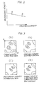
- the output from the X-ray detector 4 stored in the image memory 7 contains a two-dimensional distribution data of the characteristic X-ray peak of the element to be analyzed as shown in Fig. 3(a), and the output from the specimen current detector 5 stored in the image memory 8 contains a two dimensional distribution data of the specimen current as shown in Fig. 3(b).
- the background correcting device 10 calculates a two-dimensional distribution data of the background intensity as shown in Fig. 3(c) from the two-dimensional distribution data of the specimen current shown in Fig. 3(b). Then, the background intensity distribution data (Fig. 3(c)) is subtracted from the characteristic X-ray peak data (Fig. 3(a)) of the element being analyzed which is stored in the image memory 7 thereby to obtain a background-corrected, true distribution data of the characteristic X-ray peak of the element as shown in Fig. 3(d). The data is stored in the image memory 11 and displayed on the cathode-ray tube 12.
- the CPU 15 controls the above operations.
- the characteristic X rays are detected to provide a detection signal. It is also possible to detect secondary electrons, reflected electrons, luminescence, Auger electrons, etc. for the same purpose.
- the specimen stage is moved to scan the specimen with the electron beam. It is possible to scan the electron beam over the specimen surface.
- background correction is conducted by utilizing the specimen current detector with which conventional electron probe microanalyzers and scanning electron microscopes are usually provided, it is not necessary to add to the existing equipment any particular device for background correction. Since the measured data of the whole specimen surface to be analyzed can be accurately corrected for background by measuring background at only one or two points on the specimen surface, the time required for analysis can be greatly shortened.
Landscapes
- Chemical & Material Sciences (AREA)
- Analytical Chemistry (AREA)
- Physics & Mathematics (AREA)
- Health & Medical Sciences (AREA)
- Life Sciences & Earth Sciences (AREA)
- Biochemistry (AREA)
- General Health & Medical Sciences (AREA)
- General Physics & Mathematics (AREA)
- Immunology (AREA)
- Pathology (AREA)
- Analysing Materials By The Use Of Radiation (AREA)
Claims (11)
- Verfahren zur Hintergrundkorrektur der Meßdaten bei der Oberflächenanalyse einer Probe (S), welches die Schritte aufweist:- Bestrahlen eines vorbestimmten Bereichs der Probenoberfläche mit einem Elektronenstrahl (e), und- Erfassen eines Signals, dessen Auftreten durch Bestrahlen eines zu analysierenden Elements in der Probe (S) verursacht wird, um auf diese Weise zweidimensionale Verteilungsdaten des Signalpegels in dem bestrahlten Probenoberflächenbereich zu erhalten,dadurch gekennzeichnet, daß das Verfahren ferner die Schritte aufweist:- Erfassen eines Probenstroms, welcher in der Probe (S) durch die Bestrahlung induziert wird, um zweidimensionale Verteilungsdaten des Probenstroms in dem bestrahlten Probenoberflächenbereich zu erhalten,- Messen der Hintergrundintensität und des Werts des Probenstroms an mindestens einem Punkt in dem vorbestimmten Oberflächenbereich,- Formulieren einer Abhängigkeit zwischen der Hintergrundintensität und dem Probenstrom der Probe (S) von der Hintergrundintensität und dem Wert des Probenstroms, gemessen an mindestens einem Punkt in dem vorbestimmten Probenoberflächenbereich,- Berechnen der zweidimensionalen Verteilungsdaten der Hintergrundintensität aus den zweidimensionalen Verteilungsdaten des Probenstroms durch Verwenden der formulierten Abhängigkeit, und- Subtrahieren der berechneten zweidimensionalen Verteilungsdaten der Hintergrundintensität von den zweidimensionalen Verteilungsdaten des Signalpegels, um dadurch die zweidimensionalen Verteilungsdaten des Signalpegels mit Bezug auf den Hintergrund zu korrigieren.
- Verfahren gemäß Anspruch 1,
dadurch gekennzeichnet, daß das Signal, dessen Auftreten durch Bestrahlen eines zu analysierenden Elements in der Probe (S) mit dem Elektronenstrahl (e) verursacht wird, in der Form von Sekundärelektronen, reflektierten Elektronen, Lumineszenz, Auger-Elektronen oder Röntgenstrahlen vorliegt. - Verfahren gemäß Anspruch 1,
dadurch gekennzeichnet, daß das Bestrahlen des vorbestimmten Probenoberflächenbereichs durch Bewegen des Elektronenstrahls (e) ausgeführt wird, um auf diese Weise den vorbestimmten Probenoberflächenbereich abzutasten. - Verfahren gemäß Anspruch 1,
dadurch gekennzeichnet, daß das Bestrahlen des vorbestimmten Probenoberflächenbereichs durch Bewegen der Probe (S) ausgeführt wird, um auf diese Weise mit dem Elektronenstrahl (e) den vorbestimmten Probenoberflächenbereich abzutasten. - Verfahren gemäß Anspruch 3 oder 4,
dadurch gekennzeichnet, daß die Hintergrundintensität und der Wert des Probenstroms an einem ersten Punkt in dem vorbestimmten Probenoberflächenbereich gemessen wird, an welchem das Abtasten beginnt, und an einem zweiten Punkt, an welchem das Abtasten abgeschlossen wird. - Gerät zur Oberflächenanalyse einer Probe (S), welches aufweist:- eine Einrichtung (1) zum Erzeugen eines Elektronenstrahls (e),- eine Einrichtung zum Bestrahlen eines vorbestimmten Bereichs der Probenoberfläche mit dem Elektronenstrahl (e), und- eine erste Einrichtung (4) zum Erfassen eines Signals, dessen Auftreten durch Bestrahlen eines zu analysierenden Elements in der Probe (S) verursacht ist, um ein erstes entsprechendes Ausgabesignal zu erzeugen, welches zweidimensionale Verteilungsdaten des Signalpegels in dem bestrahlten Probenoberflächenbereich aufweist, und zum Messen der Hintergrundintensität an mindestens einem Punkt in dem vorbestimmten Probenoberflächenbereich,dadurch gekennzeichnet, daß das Gerät ferner aufweist:- eine zweite Einrichtung (5) zum Erfassen eines Probenstroms, welcher in der Probe (S) durch Bestrahlen induziert wird, um ein zweites entsprechendes Ausgabesignal zu erzeugen, welches zweidimensionale Verteilungsdaten des Probenstroms in dem bestrahlten Probenoberflächenbereich aufweist, und zum Messen des Werts des Probenstroms an mindestens einem Punkt in dem vorbestimmten Probenoberflächenbereich,- eine Einrichtung (7, 8) zum Speichern des ersten und des zweiten Ausgabesignals,- eine Einrichtung (10) zum Korrigieren des ersten Ausgabesignals für den Hintergrund durch:(a) Formulieren einer Abhängigkeit zwischen der Hintergrundintensität und dem Probenstrom der Probe (S) von dem ersten und dem zweiten Ausgabesignal, welche an mindestens einem Punkt in dem vorherbestimmten Probenoberflächenbereich erfaßt worden sind,(b) Berechnen der zweidimensionalen Verteilungsdaten der Hintergrundintensität in dem vorbestimmten Probenoberflächenbereich aus den zweidimensionalen Verteilungsdaten des Probenstroms, welche in dem zweiten Ausgabesignal enthalten sind, erfaßt in dem vorbestimmten Probenoberflächenbereich durch Verwenden der formulierten Abhängigkeit, und(c) Subtrahieren der berechneten zweidimensionalen Verteilungsdaten der Hintergrundintensität aus den zweidimensionalen Verteilungsdaten des Pegels des ersten Ausgabesignals, erfaßt in dem vorbestimmten Probenoberflächenbereich, um dadurch hintergrundkorrigierte zweidimensionale Verteilungsdaten des Pegels des ersten Ausgabesignals zu erzeugen, und- eine Einrichtung (15) zum Steuern der Bestrahlungseinrichtung, der Speichereinrichtung (7, 8) und der Hintergrund-Korrektureinrichtung (10).
- Gerät gemäß Anspruch 6,
dadurch gekennzeichnet, daß das Signal, dessen Auftreten durch Bestrahlen eines zu analysierenden Elements in der Probe (S) mit dem Elektronenstrahl (e) verursacht wird, in der Form von Sekundärelektronen, reflektierten Elektronen, Lumineszenz, Auger-Elektronen oder Röntgenstrahlen vorliegt. - Gerät gemäß Anspruch 6,
dadurch gekennzeichnet, daß die Bestrahlungseinrichtung eine Einrichtung (9) zum Bewegen der Probe (S) aufweist, so daß der Elektronenstrahl (e) den vorbestimmten Probenoberflächenbereich abtastet. - Gerät gemäß Anspruch 6,
dadurch gekennzeichnet, daß die Bestrahlungseinrichtung eine Einrichtung zum Bewegen des Elektronenstrahls (e) zum Abtasten des vorbestimmten Probenoberflächenbereichs aufweist. - Gerät gemäß Anspruch 8,
dadurch gekennzeichnet, daß die Steuereinrichtung (15) die Probenbewegungseinrichtung (9), die Speichereinrichtung (7, 8) und die Hintergrund-Korrektureinrichtung (10) steuert, so daß die Hintergrund-Korrektureinrichtung (10) eine Abhängigkeit zwischen der Hintergrundintensität und dem Probenstrom der Probe (S) von dem ersten und dem zweiten Ausgabesignal formuliert, erfaßt an einem ersten Punkt in dem vorbestimmten Probenoberflächenbereich, an welchem die Probenbewegungseinrichtung (9) den Elektronenstrahl (e) verursacht, das Abtasten des vorbestimmten Probenoberflächenbereichs zu beginnen, und an einem zweiten Punkt in dem vorbestimmten Probenoberflächenbereich, an welchem die Probenbewegungseinrichtung (9) das Beenden des Abtastens verursacht. - Gerät gemäß Anspruch 9,
dadurch gekennzeichnet, daß die Steuereinrichtung (15) die Elektronenstrahl-Bewegungseinrichtung, die Speichereinrichtung (7, 8) und die Hintergrund-Korrektureinrichtung (10) steuert, so daß die Hintergrund-Korrektureinrichtung (10) eine Abhängigkeit zwischen der Hintergrund-Intensität und dem Probenstrom der Probe (S) von dem ersten und dem zweiten Ausgabesignal formuliert, erfaßt an einem ersten Punkt in dem vorbestimmten Probenoberflächenbereich, an welchem die Elektronenstrahl-Bewegungseinrichtung den Elektronenstrahl (e) verursacht, das Abtasten des vorbestimmten Probenoberflächenbereichs zu beginnen, und an einem zweiten Punkt in dem vorbestimmten Probenoberflächenbereich, an welchem die Elektronenstrahl-Bewegungseinrichtung das Beenden des Abtastens verursacht.
Applications Claiming Priority (2)
| Application Number | Priority Date | Filing Date | Title |
|---|---|---|---|
| JP2103363A JPH07119716B2 (ja) | 1990-04-19 | 1990-04-19 | 表面分析装置 |
| JP103363/90 | 1990-04-19 |
Publications (3)
| Publication Number | Publication Date |
|---|---|
| EP0452825A2 EP0452825A2 (de) | 1991-10-23 |
| EP0452825A3 EP0452825A3 (en) | 1993-09-01 |
| EP0452825B1 true EP0452825B1 (de) | 1996-11-20 |
Family
ID=14352046
Family Applications (1)
| Application Number | Title | Priority Date | Filing Date |
|---|---|---|---|
| EP91105876A Expired - Lifetime EP0452825B1 (de) | 1990-04-19 | 1991-04-12 | Verfahren und Gerät zur Hintergrundkorrektur bei der Analyse einer Probenoberfläche |
Country Status (6)
| Country | Link |
|---|---|
| US (1) | US5128545A (de) |
| EP (1) | EP0452825B1 (de) |
| JP (1) | JPH07119716B2 (de) |
| KR (1) | KR960012331B1 (de) |
| CN (1) | CN1040251C (de) |
| DE (1) | DE69123166T2 (de) |
Families Citing this family (11)
| Publication number | Priority date | Publication date | Assignee | Title |
|---|---|---|---|---|
| US5404110A (en) * | 1993-03-25 | 1995-04-04 | International Business Machines Corporation | System using induced current for contactless testing of wiring networks |
| JP2954819B2 (ja) * | 1993-10-07 | 1999-09-27 | 株式会社東芝 | 全反射蛍光x線分析装置の校正方法 |
| US5656812A (en) * | 1995-07-21 | 1997-08-12 | Jeol Ltd. | Electron probe microanalyzer and X-ray analysis using same |
| US6118123A (en) * | 1997-02-05 | 2000-09-12 | Jeol Ltd. | Electron probe microanalyzer |
| KR100272098B1 (ko) * | 1997-07-16 | 2001-03-02 | 윤종용 | 광디스크재생장치의슬레드편차에따른슬레드모터의구동전압제어방법 |
| JP2000275197A (ja) * | 1999-03-25 | 2000-10-06 | Fuji Photo Optical Co Ltd | X線分析装置およびこれを使用した測定方法 |
| JP5039971B2 (ja) * | 2007-01-25 | 2012-10-03 | 国立大学法人東北大学 | 非走査型波長分散型x線分析装置及びそれを用いた測定方法 |
| JP5938708B2 (ja) * | 2011-10-17 | 2016-06-22 | 株式会社リガク | 蛍光x線分析用の較正試料ならびにそれを備える蛍光x線分析装置およびそれを用いる蛍光x線分析方法 |
| CN102765503B (zh) * | 2012-07-26 | 2013-12-18 | 武汉钢铁(集团)公司 | 彩涂钢卷连续在线贴膜及卷取工艺 |
| US11054375B2 (en) | 2016-09-15 | 2021-07-06 | University Of Washington | X-ray spectrometer and methods for use |
| CN107091622B (zh) * | 2017-06-24 | 2020-01-10 | 福建省南安市清信石材有限公司 | 一种纳米分辨率的应变测试设备及方法 |
Family Cites Families (10)
| Publication number | Priority date | Publication date | Assignee | Title |
|---|---|---|---|---|
| JPS5481075A (en) * | 1977-11-24 | 1979-06-28 | Cho Lsi Gijutsu Kenkyu Kumiai | Method of detecting article image using electron beam |
| SU1250925A1 (ru) * | 1984-05-11 | 1986-08-15 | Иркутский государственный университет им.А.А.Жданова | Способ рентгеноспектрального флуоресцентного анализа сплавов |
| SU1224688A1 (ru) * | 1984-07-20 | 1986-04-15 | Казанский Ордена Трудового Красного Знамени Государственный Университет Им.С.М.Кирова | Способ определени фона в рентгенофлуоресцентном анализе сложных по составу сред |
| EP0196804B1 (de) * | 1985-03-11 | 1991-01-23 | Nippon Telegraph And Telephone Corporation | Methode und Gerät zum Testen eines integrierten elektronischen Bauteils |
| EP0204855B1 (de) * | 1985-06-11 | 1992-03-04 | Shimadzu Corporation | Verfahren und Vorrichtung zur Zustandsanalyse |
| US4697080A (en) * | 1986-01-06 | 1987-09-29 | The United States Of America As Represented By The United States Department Of Energy | Analysis with electron microscope of multielement samples using pure element standards |
| JPS6385860U (de) * | 1986-11-26 | 1988-06-04 | ||
| JPS63313043A (ja) * | 1987-06-15 | 1988-12-21 | Jeol Ltd | 平均原子番号によるバックグラウンド推定法 |
| CN1012704B (zh) * | 1988-05-16 | 1991-05-29 | 中国科学院长春光学精密机械研究所 | 双通道比率记录中的串扰补偿方法及装置 |
| JP2842879B2 (ja) * | 1989-01-06 | 1999-01-06 | 株式会社日立製作所 | 表面分析方法および装置 |
-
1990
- 1990-04-19 JP JP2103363A patent/JPH07119716B2/ja not_active Expired - Fee Related
-
1991
- 1991-04-04 US US07/680,427 patent/US5128545A/en not_active Expired - Fee Related
- 1991-04-12 DE DE69123166T patent/DE69123166T2/de not_active Expired - Fee Related
- 1991-04-12 EP EP91105876A patent/EP0452825B1/de not_active Expired - Lifetime
- 1991-04-13 CN CN91102529A patent/CN1040251C/zh not_active Expired - Fee Related
- 1991-04-15 KR KR1019910006030A patent/KR960012331B1/ko not_active Expired - Fee Related
Also Published As
| Publication number | Publication date |
|---|---|
| KR960012331B1 (ko) | 1996-09-18 |
| JPH042955A (ja) | 1992-01-07 |
| JPH07119716B2 (ja) | 1995-12-20 |
| EP0452825A2 (de) | 1991-10-23 |
| DE69123166D1 (de) | 1997-01-02 |
| KR910018798A (ko) | 1991-11-30 |
| CN1040251C (zh) | 1998-10-14 |
| EP0452825A3 (en) | 1993-09-01 |
| US5128545A (en) | 1992-07-07 |
| DE69123166T2 (de) | 1997-04-10 |
| CN1055998A (zh) | 1991-11-06 |
Similar Documents
| Publication | Publication Date | Title |
|---|---|---|
| US4037101A (en) | Method and apparatus for analyzing fine grained substances | |
| KR19980070850A (ko) | 시료 분석 장치 | |
| EP0452825B1 (de) | Verfahren und Gerät zur Hintergrundkorrektur bei der Analyse einer Probenoberfläche | |
| US20080181458A1 (en) | Light intensity measurement method and light intensity measurement system | |
| US7579591B2 (en) | Method and apparatus for analyzing sample | |
| JPH05101800A (ja) | 電子ミクロ分析方式における標的領域をサンプル表面上に求める方式 | |
| JP2001307672A (ja) | 元素分析装置及び走査透過型電子顕微鏡並びに元素分析方法 | |
| EP3633361B1 (de) | Verfahren zur erzeugung einer elementaren karte und oberflächenanalysator | |
| JPH1027833A (ja) | 異物分析方法 | |
| JP3454052B2 (ja) | 電子線分析装置 | |
| JP2002157973A (ja) | エネルギースペクトル測定装置,電子エネルギー損失分光装置、及びそれを備えた電子顕微鏡、及び電子エネルギー損失スペクトル測定方法 | |
| JP2002286663A (ja) | 試料分析および試料観察装置 | |
| US20030085350A1 (en) | Ultimate analyzer, scanning transmission electron microscope and ultimate analysis method | |
| US20240142395A1 (en) | Analyzing Method and Analyzer | |
| WO2013084905A1 (ja) | X線分析装置 | |
| JP2004265879A (ja) | 元素マッピング装置,走査透過型電子顕微鏡および元素マッピング方法 | |
| JP2001099795A (ja) | 元素マッピング装置 | |
| JP2564896B2 (ja) | X線分光マッピング装置 | |
| JP2002062270A (ja) | 電子線を用いた表面分析装置における面分析データ表示方法 | |
| JP3790643B2 (ja) | エネルギー分散形x線検出器を備えた表面分析装置 | |
| JPS62285048A (ja) | 元素濃度分布測定方法 | |
| JP2002310957A (ja) | 電子励起によるx線分析装置 | |
| WO2025094225A1 (ja) | 画像処理方法、プログラム、画像処理装置、およびイメージング質量分析装置 | |
| JPH10213556A (ja) | 表面元素分析装置及び分析方法 | |
| US20260002895A1 (en) | Evaluation Method and Analyzer Apparatus |
Legal Events
| Date | Code | Title | Description |
|---|---|---|---|
| PUAI | Public reference made under article 153(3) epc to a published international application that has entered the european phase |
Free format text: ORIGINAL CODE: 0009012 |
|
| AK | Designated contracting states |
Kind code of ref document: A2 Designated state(s): DE FR GB |
|
| 17P | Request for examination filed |
Effective date: 19921228 |
|
| PUAL | Search report despatched |
Free format text: ORIGINAL CODE: 0009013 |
|
| AK | Designated contracting states |
Kind code of ref document: A3 Designated state(s): DE FR GB |
|
| 17Q | First examination report despatched |
Effective date: 19941006 |
|
| GRAG | Despatch of communication of intention to grant |
Free format text: ORIGINAL CODE: EPIDOS AGRA |
|
| GRAH | Despatch of communication of intention to grant a patent |
Free format text: ORIGINAL CODE: EPIDOS IGRA |
|
| GRAH | Despatch of communication of intention to grant a patent |
Free format text: ORIGINAL CODE: EPIDOS IGRA |
|
| GRAA | (expected) grant |
Free format text: ORIGINAL CODE: 0009210 |
|
| AK | Designated contracting states |
Kind code of ref document: B1 Designated state(s): DE FR GB |
|
| REF | Corresponds to: |
Ref document number: 69123166 Country of ref document: DE Date of ref document: 19970102 |
|
| ET | Fr: translation filed | ||
| PLBE | No opposition filed within time limit |
Free format text: ORIGINAL CODE: 0009261 |
|
| STAA | Information on the status of an ep patent application or granted ep patent |
Free format text: STATUS: NO OPPOSITION FILED WITHIN TIME LIMIT |
|
| 26N | No opposition filed | ||
| PGFP | Annual fee paid to national office [announced via postgrant information from national office to epo] |
Ref country code: DE Payment date: 20010330 Year of fee payment: 11 |
|
| PGFP | Annual fee paid to national office [announced via postgrant information from national office to epo] |
Ref country code: FR Payment date: 20010409 Year of fee payment: 11 |
|
| PGFP | Annual fee paid to national office [announced via postgrant information from national office to epo] |
Ref country code: GB Payment date: 20010411 Year of fee payment: 11 |
|
| REG | Reference to a national code |
Ref country code: GB Ref legal event code: IF02 |
|
| PG25 | Lapsed in a contracting state [announced via postgrant information from national office to epo] |
Ref country code: GB Free format text: LAPSE BECAUSE OF NON-PAYMENT OF DUE FEES Effective date: 20020412 |
|
| PG25 | Lapsed in a contracting state [announced via postgrant information from national office to epo] |
Ref country code: DE Free format text: LAPSE BECAUSE OF NON-PAYMENT OF DUE FEES Effective date: 20021101 |
|
| GBPC | Gb: european patent ceased through non-payment of renewal fee |
Effective date: 20020412 |
|
| PG25 | Lapsed in a contracting state [announced via postgrant information from national office to epo] |
Ref country code: FR Free format text: LAPSE BECAUSE OF NON-PAYMENT OF DUE FEES Effective date: 20021231 |
|
| REG | Reference to a national code |
Ref country code: FR Ref legal event code: ST |