EP0453310A1 - Masque pour photolithographie - Google Patents
Masque pour photolithographie Download PDFInfo
- Publication number
- EP0453310A1 EP0453310A1 EP91303545A EP91303545A EP0453310A1 EP 0453310 A1 EP0453310 A1 EP 0453310A1 EP 91303545 A EP91303545 A EP 91303545A EP 91303545 A EP91303545 A EP 91303545A EP 0453310 A1 EP0453310 A1 EP 0453310A1
- Authority
- EP
- European Patent Office
- Prior art keywords
- film
- pattern
- mask
- substrate
- transparent
- Prior art date
- Legal status (The legal status is an assumption and is not a legal conclusion. Google has not performed a legal analysis and makes no representation as to the accuracy of the status listed.)
- Granted
Links
- 238000000206 photolithography Methods 0.000 title claims abstract description 10
- 239000000758 substrate Substances 0.000 claims abstract description 57
- 238000004519 manufacturing process Methods 0.000 claims abstract description 22
- 239000004065 semiconductor Substances 0.000 claims abstract description 8
- 230000002401 inhibitory effect Effects 0.000 claims abstract 2
- 238000000034 method Methods 0.000 claims description 48
- 238000005530 etching Methods 0.000 claims description 37
- VYPSYNLAJGMNEJ-UHFFFAOYSA-N silicon dioxide Inorganic materials O=[Si]=O VYPSYNLAJGMNEJ-UHFFFAOYSA-N 0.000 claims description 24
- 238000010894 electron beam technology Methods 0.000 claims description 22
- 239000010453 quartz Substances 0.000 claims description 18
- 239000011651 chromium Substances 0.000 claims description 10
- VYZAMTAEIAYCRO-UHFFFAOYSA-N Chromium Chemical compound [Cr] VYZAMTAEIAYCRO-UHFFFAOYSA-N 0.000 claims description 9
- 229910052804 chromium Inorganic materials 0.000 claims description 9
- XUIMIQQOPSSXEZ-UHFFFAOYSA-N Silicon Chemical compound [Si] XUIMIQQOPSSXEZ-UHFFFAOYSA-N 0.000 claims description 8
- 238000000151 deposition Methods 0.000 claims description 8
- 229910052751 metal Inorganic materials 0.000 claims description 8
- 239000002184 metal Substances 0.000 claims description 8
- PXHVJJICTQNCMI-UHFFFAOYSA-N Nickel Chemical compound [Ni] PXHVJJICTQNCMI-UHFFFAOYSA-N 0.000 claims description 6
- 229910052710 silicon Inorganic materials 0.000 claims description 5
- 239000010703 silicon Substances 0.000 claims description 5
- 229910000676 Si alloy Inorganic materials 0.000 claims description 3
- 229910052782 aluminium Inorganic materials 0.000 claims description 3
- XAGFODPZIPBFFR-UHFFFAOYSA-N aluminium Chemical compound [Al] XAGFODPZIPBFFR-UHFFFAOYSA-N 0.000 claims description 3
- 229910017052 cobalt Inorganic materials 0.000 claims description 3
- 239000010941 cobalt Substances 0.000 claims description 3
- GUTLYIVDDKVIGB-UHFFFAOYSA-N cobalt atom Chemical compound [Co] GUTLYIVDDKVIGB-UHFFFAOYSA-N 0.000 claims description 3
- 229910052759 nickel Inorganic materials 0.000 claims description 3
- WFKWXMTUELFFGS-UHFFFAOYSA-N tungsten Chemical compound [W] WFKWXMTUELFFGS-UHFFFAOYSA-N 0.000 claims description 3
- 229910052721 tungsten Inorganic materials 0.000 claims description 3
- 239000010937 tungsten Substances 0.000 claims description 3
- 230000005855 radiation Effects 0.000 claims 2
- 230000000903 blocking effect Effects 0.000 claims 1
- 238000010030 laminating Methods 0.000 claims 1
- 238000000059 patterning Methods 0.000 claims 1
- 230000010363 phase shift Effects 0.000 claims 1
- 239000012780 transparent material Substances 0.000 claims 1
- 239000010408 film Substances 0.000 description 110
- 239000012071 phase Substances 0.000 description 57
- 235000012239 silicon dioxide Nutrition 0.000 description 18
- 239000010410 layer Substances 0.000 description 15
- 239000000463 material Substances 0.000 description 12
- 239000011521 glass Substances 0.000 description 8
- 239000007791 liquid phase Substances 0.000 description 8
- 238000011161 development Methods 0.000 description 6
- 238000002360 preparation method Methods 0.000 description 6
- 238000004528 spin coating Methods 0.000 description 6
- 239000010409 thin film Substances 0.000 description 6
- ZOKXTWBITQBERF-UHFFFAOYSA-N Molybdenum Chemical compound [Mo] ZOKXTWBITQBERF-UHFFFAOYSA-N 0.000 description 4
- BLRPTPMANUNPDV-UHFFFAOYSA-N Silane Chemical compound [SiH4] BLRPTPMANUNPDV-UHFFFAOYSA-N 0.000 description 4
- HIVGXUNKSAJJDN-UHFFFAOYSA-N [Si].[P] Chemical compound [Si].[P] HIVGXUNKSAJJDN-UHFFFAOYSA-N 0.000 description 4
- MXSJNBRAMXILSE-UHFFFAOYSA-N [Si].[P].[B] Chemical compound [Si].[P].[B] MXSJNBRAMXILSE-UHFFFAOYSA-N 0.000 description 4
- 230000015572 biosynthetic process Effects 0.000 description 4
- 229910052750 molybdenum Inorganic materials 0.000 description 4
- 239000011733 molybdenum Substances 0.000 description 4
- VZGDMQKNWNREIO-UHFFFAOYSA-N tetrachloromethane Chemical compound ClC(Cl)(Cl)Cl VZGDMQKNWNREIO-UHFFFAOYSA-N 0.000 description 4
- QVGXLLKOCUKJST-UHFFFAOYSA-N atomic oxygen Chemical compound [O] QVGXLLKOCUKJST-UHFFFAOYSA-N 0.000 description 3
- 230000008021 deposition Effects 0.000 description 3
- 238000010586 diagram Methods 0.000 description 3
- 230000004907 flux Effects 0.000 description 3
- 239000007789 gas Substances 0.000 description 3
- 229910052760 oxygen Inorganic materials 0.000 description 3
- 239000001301 oxygen Substances 0.000 description 3
- 238000001020 plasma etching Methods 0.000 description 3
- 238000012545 processing Methods 0.000 description 3
- 239000012808 vapor phase Substances 0.000 description 3
- 229910052581 Si3N4 Inorganic materials 0.000 description 2
- 229910008814 WSi2 Inorganic materials 0.000 description 2
- YXTPWUNVHCYOSP-UHFFFAOYSA-N bis($l^{2}-silanylidene)molybdenum Chemical compound [Si]=[Mo]=[Si] YXTPWUNVHCYOSP-UHFFFAOYSA-N 0.000 description 2
- 230000001747 exhibiting effect Effects 0.000 description 2
- 238000005268 plasma chemical vapour deposition Methods 0.000 description 2
- 229920000642 polymer Polymers 0.000 description 2
- 239000012495 reaction gas Substances 0.000 description 2
- 229910000077 silane Inorganic materials 0.000 description 2
- HQVNEWCFYHHQES-UHFFFAOYSA-N silicon nitride Chemical compound N12[Si]34N5[Si]62N3[Si]51N64 HQVNEWCFYHHQES-UHFFFAOYSA-N 0.000 description 2
- 239000002356 single layer Substances 0.000 description 2
- 238000012360 testing method Methods 0.000 description 2
- 239000010936 titanium Substances 0.000 description 2
- WQJQOUPTWCFRMM-UHFFFAOYSA-N tungsten disilicide Chemical compound [Si]#[W]#[Si] WQJQOUPTWCFRMM-UHFFFAOYSA-N 0.000 description 2
- 229910021342 tungsten silicide Inorganic materials 0.000 description 2
- 238000005406 washing Methods 0.000 description 2
- XPDWGBQVDMORPB-UHFFFAOYSA-N Fluoroform Chemical compound FC(F)F XPDWGBQVDMORPB-UHFFFAOYSA-N 0.000 description 1
- RTAQQCXQSZGOHL-UHFFFAOYSA-N Titanium Chemical compound [Ti] RTAQQCXQSZGOHL-UHFFFAOYSA-N 0.000 description 1
- WGLPBDUCMAPZCE-UHFFFAOYSA-N Trioxochromium Chemical compound O=[Cr](=O)=O WGLPBDUCMAPZCE-UHFFFAOYSA-N 0.000 description 1
- 238000013459 approach Methods 0.000 description 1
- 229910000423 chromium oxide Inorganic materials 0.000 description 1
- 239000011248 coating agent Substances 0.000 description 1
- 238000000576 coating method Methods 0.000 description 1
- 239000006185 dispersion Substances 0.000 description 1
- QSHDDOUJBYECFT-UHFFFAOYSA-N mercury Chemical compound [Hg] QSHDDOUJBYECFT-UHFFFAOYSA-N 0.000 description 1
- 229910021344 molybdenum silicide Inorganic materials 0.000 description 1
- 239000002245 particle Substances 0.000 description 1
- 239000011347 resin Substances 0.000 description 1
- 229920005989 resin Polymers 0.000 description 1
- 239000000377 silicon dioxide Substances 0.000 description 1
- 229910052814 silicon oxide Inorganic materials 0.000 description 1
- 229910052719 titanium Inorganic materials 0.000 description 1
Images

Classifications
-
- G—PHYSICS
- G03—PHOTOGRAPHY; CINEMATOGRAPHY; ANALOGOUS TECHNIQUES USING WAVES OTHER THAN OPTICAL WAVES; ELECTROGRAPHY; HOLOGRAPHY
- G03F—PHOTOMECHANICAL PRODUCTION OF TEXTURED OR PATTERNED SURFACES, e.g. FOR PRINTING, FOR PROCESSING OF SEMICONDUCTOR DEVICES; MATERIALS THEREFOR; ORIGINALS THEREFOR; APPARATUS SPECIALLY ADAPTED THEREFOR
- G03F1/00—Originals for photomechanical production of textured or patterned surfaces, e.g., masks, photo-masks, reticles; Mask blanks or pellicles therefor; Containers specially adapted therefor; Preparation thereof
- G03F1/26—Phase shift masks [PSM]; PSM blanks; Preparation thereof
- G03F1/29—Rim PSM or outrigger PSM; Preparation thereof
Definitions
- the present invention relates to a mask used in a photolithographic system in fabrication of semiconductor devices and the like.
- ULSI semiconductor devices which have been produced in recent years assemble a large number of transistors and wirings in micron on a single silicon substrate.
- a photolithographic technology such as stepper (step and repeat photolithographic system with demagnification), transferring a mask's pattern in a reduced size (usually to one fifth) onto a photosensitive resin (resist) layer formed on the silicon substrate of the semiconductor devices.
- the photolithographic system (the stepper) which is now applied to mass production of 1MB and 4MB DRAM devices uses the mask patterns having the respective minimum line widths of 1.2 and 0.8 ⁇ m for each DRAM device, and generally adopts emission lines called g-light of 436nm emitted by and ultra high-pressure mercury-vapor lamp, while emission lines called i-light of 365nm emitted by the same lamp has been locally used.
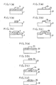
- the phase shifting mask also has an opening 54 provided as conventionally and fine apertures 55 adjacent to the opening 54. The fine apertures 55, 55′ do not dissect image by themselves and are disposed with the phase shifting film 53.
- Light from the opening 54 is shifted by 180° relative to light from the apertures 55, so that light wave diffracted from the opening 54 to its adjacent area is offset with light wave from the apertures 55. Accordingly, light on the projection area is restrained from effusing from the opening 54 to its adjacent area, thereby improving contrast of the projected image.
- the phase shifting mask improves contrast of image projected on the resist layer to have the practical resolution largely improved.
- a first resist image for a chromium pattern is first drawn by use of electron beam lithographic system, and a second resist image is then drawn for defining a phase shifting film.
- the system has to conduct twice the electron beam drawing which takes longer time and also to align the first pattern with the second pattern with high accuracy, leading to a complex and expensive technology for preparation of mask.
- phase shifting mask shown in Fig. 6 which comprises a transparent quartz substrate 61 to admit applied light of any wavelengths, a chromium film 62 obstructing the applied light and a phase shifting film 63 whose thickness satisfies the relationship of the foregoing formula (1).
- an opening 64 is first formed in a resist film (not shown) by use of electron beam lithographic system and the chromium film 62 is then etched and removed at the part of the opening 64, while the resist film is also removed.
- a resist film for forming the phase shifting film 63 is formed and ultraviolet is applied from the back of the substrate to the resist film at the opening 64 which resist film is then developed and removed.
- the chromium film 62 is etched partially under the resist film to have an opening larger than the opening 64 and having a region 65 over which the resist film hangs. Light passing through the region 65 and that passing through the opening 64 are different in phase at 180° from each other, so that both light is offset with each other when they are overlapped in a projected image, thereby preventing the light from effusing from the region 64 to its adjacent part. Hence, dispersion of photo-intensity on an image formation surface is sharp to improve the practical resolution of photolithography.
- the preparation method for this phase shifting mask does not need to increase times of drawing by electron beam lithographic system, in turn, the number of steps for preparation of the mask.
- the resist film kept for forming the phase shifting film is fragile, it is hard to wash and remove foreign particles on the mask. Thus, the method is not practical.
- phase shifting masks as discussed above or related there are disclosed in e.g.,
- Japanese Patent Publication No. 62(1987)-50811 Japanese Unexamined Patent Publication Nos. 58(1983)-173744, 62(1987)-67514, 1(1990)-147457 & 1(1990)-283925 and IEDM 1989, p57 (New Phase Shifting Mask with Self-aligned Phase Shifters for a Quarter Micron Photolithography).
- phase shifting mask previously proposed has the above problems in the aspect of practical use, and any phase shifting masks simple in fabrication and having sufficient durability have been expected.
- the present invention provides a phase shifting mask for photolithography which comprises a transparent substrate to admit light of predetermined wavelengths(e.g., visible light or ultraviolet) for transferring a mask pattern which is opaque not to admit the light and formed on the substrate, a transparent portion adjacent to the opaque pattern is provided with a stepped portion having an inclined area, thereby providing a phase shifting mask simply fabricated and having durability.
- the present invention also provides a process for the preparation of the above phase shifting mask.
- Figs. 1 (a) to (c), Figs. 2 (a) to (c), Figs. 3 (a) to (d), Figs. 4 (a) to (d), Figs. 7 (a) to (c) and Figs. 8 (a) to (c) are schematic diagrams showing the fabrication processes of the mask in the six examples of the present invention.
- Figs. 5 and 6 are schematic diagrams showing the problematic points in the conventional phase shifting masks.
- Fig. 9 is a schematic diagram showing the thickness of the SOG film.
- the stepped portion having the inclined area is formed to a height approaching the foregoing formula (1).
- a transparent film is formed to a thickness approaching the height of the stepped portion on an opaque pattern of relatively larger thickness in accordance with vapor phase CVD process, or by spin coating.
- the opaque pattern may be a thin film of single phase or a multi-layer of a thin opaque film and a transparent film or a resist pattern.
- the opaque pattern may be provided on the transparent substrate or by etching the transparent substrate.
- the stepped portion having the inclined area is formed by depositing or applying a transparent film of a thickness approaching the foregoing formula (1) on an opaque pattern of relatively larger thickness in accordance with vapor phase CVD process, or by spin coating followed by anisotropic etching to leave the transparent film on the side wall of the opaque pattern.
- the opaque pattern may be a thin film of single phase or a multi-layer of a thin opaque film and a transparent film.
- the opaque pattern may be provided on the transparent substrate or by etching the transparent substrate.
- the stepped portion having the inclined area may be formed by etching the opaque film of the opaque pattern and then tapering the surface of the transparent substrate to the thickness approaching the foregoing formula (1).
- phase shifting region comprises a film deposited by CVD process or formed by spin coating or the transparent substrate itself, so that the region will be not damaged by the washing step of the mask and the like.
- the mask of the present invention provides the inclined area on the border between the transparent region and the opaque region to allow phase shifting of the light passing through the phase shifting region to increase continuously from the transparent region to the opaque region. Hence, when the phase shifting at the edge of the transparent region is set to a value approaching 180°, the light passing through the transparent region is not unexpectedly decayed and only the edge of light flux passing through the transparent region can be sharply shaped up.
- a shield film 2 was deposited on a substrate 1 made of quartz, on which a resist layer to electron beam was formed followed by drawing thereon a predetermined pattern by use of an electron beam lithographic apparatus before development to obtain a resist pattern 3 (see Fig. 1(a)).
- the shield film 2 was then etched by anisotropic etching using the resist pattern 3 as a mask to form an opaque pattern 4 followed by removing the resist layer (see Fig. 1(b)).
- the method in this example shapes the end of the opaque pattern 4 at an angle as extending almost vertically and the CVD film deposited on the stepped side wall portion by CVD process is used as the phase shifting film.
- the profile of the CVD film is a quarter arc as seen in Fig. 1(c) and the portion of the CVD film denoted by 6 serves as the phase shifting region.
- an effective thickness of the phase shifting region at the edge of the opaque pattern is almost equal to that of the opaque pattern.
- the thickness of the shield film 2 was set in accordance with the foregoing formula (1). Lengths of the phase shifting region which has a relationship with the thickness of the transparent film 5 deposited on the side wall may be selectively set corresponding to the thickness of the transparent film 5. To be especially noted is the thickness of the stepped portion of the transparent film 5 which is likely to be thinner than the flat portion or varies depending on various CVD processes or systems applied.
- a double-layered metal film made of molybdenum(Mo)/Titanium(Ti) of 400nm in total thickness was used as the shield film.
- Etching was conducted by use of reactive ion-etching system having parallel plates electrodes using reaction gas of carbon tetrachloride (CCl4) + oxygen (O2).
- Applied as the transparent CVD film was silicon oxide film (SiO2) of 400nm formed by normal pressure CVD process using material gas of silane (SiH4) + oxygen (O2).
- the thickness of oxide film on the side wall portion was about 300nm.
- Exposure test was conducted by use of the stepper with i-light of 0.45 of NA and using the phase shifting mask fabricated with the materials and the steps.
- phase shifting mask obtained in the present example had the line/space resolution of 0.35 ⁇ m improved more than 10% than the conventional mask exhibiting this resolution of 0.4 ⁇ m.
- the shield film may be a metal film made of tungsten, chromium, cobalt, nickel, aluminum or the like, a silicon metal compound made of tungsten silicide (WSi2), molybdenum silicide (MoSi2y) or the like, or a semiconductor film made of silicon alloy, silicon or the like. Any suitable etching techniques other than reactive ion etching may be applied depending on the material of the shield film.
- the shield film when using a metal such as molybdenum or the like may provide a pattern with the edge being inclined almost at 90° by use of liquid phase etching.
- the transparent film may be a thin transparent film made of silicon-phosphorus glass, silicon-phosphorus-boron glass, silicon nitride or the like. Deposition may be conducted by reduced pressure CVD process, plasma CVD process or the like other than normal pressure CVD process. Furthermore, the transparent film may be a thin transparent film made of silicon-phosphorus glass, silicon-phosphorus-boron glass or the like formed by spin coating.
- the shield film is not limited to a single opaque film and may be multi-layered with a transparent film and an opaque film.
- the transparent film is not limited to a single layer and may be multi-layered.
- a shield film 72 was deposited on a substrate 71 made of quartz, on which a resist layer to electron beam was formed followed by drawing thereon a predetermined pattern by use of electron beam lithographic system before development to obtain a resist pattern 73 (see Fig. 7(a)).
- the shield film 72 was then etched by normal liquid phase etching using the resist pattern 73 as a mask to form an opaque pattern 74.(see Fig. 7(b)).
- the second example had the same result as that of Example 1.
- the transparent film may be a thin transparent film made of silicon-phosphorus glass, silicon-phosphorus-boron glass, silicon nitride or the like other than the above SiO2. Deposition may be conducted by reduced pressure CVD process, plasma CVD process or the like other than normal pressure CVD process. Furthermore, the shield film may be formed by selectively using various material, fabrication techniques and processing similarly with Example 1.
- a shield film 82 was deposited on a substrate 81 made of quartz, on which a resist layer to electron beam was formed followed by drawing thereon a predetermined pattern by use of electron beam lithographic system before development to obtain a resist pattern 83 (see Fig. 8(a)).
- the shield film 82 was then etched by normal liquid phase etching using the resist pattern 83 as a mask to form an opaque pattern 84.(see Fig. 8(b)).
- the edge of the resist pattern 83 and the opaque pattern 84 have preferably an angle as extending almost vertically.
- the combination of the material for resist layer and SOG solution must not dissolve the resist layer upon coating of SOG solution.
- the SOG film at the stepped portion has an inclined feature as seen in Fig. 8(c), and the portion of the SOG film denoted by 86 serves as the phase shifting region.
- the maximum thickness Tm of the phase shifting region formed by spin coating of transparent SOG has a relationship with respect to difference of height Td between the opaque pattern part and the transparent part, the thickness of SOG film T top on the opaque pattern part and the thickness of SOG film T bot on the transparent part (see Fig.
- Tm Td + T top - T bot
- the maximum thickness Tm of the phase shifting region is preferably almost equal to the thickness Ts of phase shifting film shown in the foregoing formula (1).
- a phase shifting mask for the stepper with i-light (365nm) in this example a posi-type resist of 500nm was used for a resist layer forming the pattern of the shield film, and a double-layered metal film of chromium oxide/chromium (Cr) of 100nm of total thickness was applied for the shield film. Etching of the shield film was conducted by normal liquid phase etching.
- Transparent SOG film of 1.46 of refractivity was applied by spin coating to obtain a phase shifting region in 300nm of T bot , 400nm of Tm and 100nm of T top .
- the specific techniques for these processes are known in the art of fabrication of IC.
- Exposure test was conducted by use of the stepper with 0.45 of NA using the phase shifting mask fabricated with the above materials and the steps.
- the phase shifting mask obtained in the present example had the line/space resolution of 0.35 ⁇ m improved more than 10% than the conventional mask exhibiting this resolution of 0.4 ⁇ m.
- the shielding film may be a metal film made of molybdenum, tungsten, chromium, cobalt, nickel, aluminum or the like, a silicon metal compound made of tungsten silicide (WSi2), molybdenum silicide (MoSi2) or the like, or a semiconductor film made of silicon alloy, silicon or the like. Any suitable etching techniques other than normal liquid phase etching may be applied depending on the material of the shielding film.
- the shielding film when using a metal such as molybdenum or the like may provide a pattern with the edge being inclined almost at 90° by use of reactive ion etching.
- the transparent film may be a thin transparent film made of silicon-phosphorus glass, silicon-phosphorus-boron glass, or the like.
- the shield film is not limited to a single opaque film and may be multi-layered with a transparent film and an opaque film.
- the transparent film is not limited to a single layer and may be multi-layered.
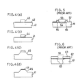
- the fourth example is different from Example 1 in that the surface of the substrate is etched to form a stepped portion.
- a shield film 22 was deposited on a substrate 21 made of quartz, on which a resist layer to electron beam was formed followed by drawing thereon a predetermined pattern by use of electron beam lithographic system before development to obtain a resist pattern 23 (see Fig. 2(a)).
- the shield film 22 was then etched by normal liquid phase etching using the resist pattern 23 as a mask to form an opaque pattern 24. Also, the quartz substrate 21 was etched by reactive etching using the resist pattern 23 as a mask to form a pattern 25 followed by removing the resist pattern 23 (see Fig. 2(b)).
- the effective thickness of the phase shifting region on the edge of the opaque pattern is almost equal to the height of the opaque pattern part, so that an amount of etching on the substrate was set to that obtained by deducting the thickness of the shield film 22 from the height of phase shifting region determined by the foregoing formula (1). Also, lengths of the phase shifting region which vary depending on the thickness of the transparent film 26 deposited on the side wall portion are adjusted corresponding to the thickness of the transparent film 26.
- Material for the shield film, transparent film and the like, and fabrication and processing techniques thereof may be variously selected as in Example 1.
- the fifth example is different from Example 1 in that the transparent film is first deposited followed by etching the transparent film at the flat portion in accordance with anisotropic etching to leave the transparent film only on the side wall part of the opaque pattern.
- a shield film 32 was deposited on a substrate 31 made of quartz, on which a resist layer to electron beam was formed followed by drawing thereon a predetermined pattern by use of electron beam lithographic system before development to obtain a resist pattern 33 (see Fig. 3(a)).
- the shield film 32 was then etched by normal liquid phase etching using the resist pattern 33 as a mask to form an opaque pattern 34 followed by removing the resist pattern 33 (see Fig. 3(b)).
- the transparent film 35 was etched back by reactive etching to leave the transparent film only on the side wall part to form a phase shifting region 36 before completion of the mask fabrication process (see Fig. 3(c)).
- Material for the shield film, transparent film and the like, and fabrication and processing techniques thereof may be variously selected as in Example 1.
- the sixth example is different from Example 1 in that an inclined area is formed on the border between the transparent part and the opaque part in the step of etching of the opaque pattern.
- a shield film 42 was deposited on a substrate 41 made of quartz, on which a resist layer to electron beam was formed followed by drawing thereon a predetermined pattern by use of electron beam lithographic system before development to obtain a resist pattern 43 (see Fig. 4(a)).
- the shield film 42 was then etched by normal liquid phase etching using the resist pattern 43 as a mask to form an opaque pattern 44 (see Fig. 4(b)).
- the quartz substrate 41 was etched by reactive etching using the resist pattern 43 as a mask to form a pattern 45.
- the pattern In the etching, the pattern must become larger as etching is proceeded.
- Etching of silicon dioxide is conducted generally by using reaction gas mainly made of CF4 + H2 or CHF3. The gas is likely to form polymer in vapor phase.
- reaction gas mainly made of CF4 + H2 or CHF3.
- the gas is likely to form polymer in vapor phase.
- polymer is deposited on the side wall part to make thicker the resultant pattern and taper the etched part during etching.
- the known etching technique forms the inclined area 45 on the quartz substrate adjacent to the opaque region. (see Fig. 4(c)).
- the present invention provides a mask for photolithography which comprises a transparent substrate to admit visible light or ultraviolet for transferring a mask pattern which is opaque not to admit the light and formed on the substrate, wherein a stepped portion having an inclined area is provided on the transparent part adjacent to the opaque pattern, so that drawing of the pattern by electron beam lithographic system is required only once, thereby allowing formation of a self-aligned phase shifting region.
- the phase shifting part is made of a SOG film, a CVD deposition film or the transparent substrate itself, thereby having little fear of being damaged in washing process or the like.
- the inclined area formed on the border between the transparent part and the opaque part allows phase shifting of light passing through the phase shifting part to be continuously increased from the transparent part to the opaque part.
- phase shifting at the edge of the transparent part is set to a value approaching 180°, only the edge part of light flux passing through the transparent part can be sharply shaped up without unexpectedly decaying the applied light as a whole, leading to a remarkable improvement of the resolution of photolithography in comparison with the conventional phase shifting mask.
Landscapes
- Physics & Mathematics (AREA)
- General Physics & Mathematics (AREA)
- Preparing Plates And Mask In Photomechanical Process (AREA)
Applications Claiming Priority (6)
| Application Number | Priority Date | Filing Date | Title |
|---|---|---|---|
| JP10583290 | 1990-04-19 | ||
| JP105832/90 | 1990-04-19 | ||
| JP10583290 | 1990-04-19 | ||
| JP17192090 | 1990-06-28 | ||
| JP17192090A JP2566048B2 (ja) | 1990-04-19 | 1990-06-28 | 光露光用マスク及びその製造方法 |
| JP171920/90 | 1991-06-18 |
Publications (2)
| Publication Number | Publication Date |
|---|---|
| EP0453310A1 true EP0453310A1 (fr) | 1991-10-23 |
| EP0453310B1 EP0453310B1 (fr) | 2000-07-12 |
Family
ID=26446055
Family Applications (1)
| Application Number | Title | Priority Date | Filing Date |
|---|---|---|---|
| EP91303545A Expired - Lifetime EP0453310B1 (fr) | 1990-04-19 | 1991-04-19 | Masque pour photolithographie |
Country Status (5)
| Country | Link |
|---|---|
| US (1) | US5389474A (fr) |
| EP (1) | EP0453310B1 (fr) |
| JP (1) | JP2566048B2 (fr) |
| KR (1) | KR940007788B1 (fr) |
| DE (1) | DE69132303T2 (fr) |
Cited By (6)
| Publication number | Priority date | Publication date | Assignee | Title |
|---|---|---|---|---|
| EP0475694A3 (en) * | 1990-09-10 | 1992-09-16 | Fujitsu Limited | Optical mask using phase shift and method of producing the same |
| EP0524741A1 (fr) * | 1991-07-12 | 1993-01-27 | Motorola, Inc. | Méthode pour améliorer la résolution d'un masque servant à la fabrication de semi-conducteurs |
| DE4229157A1 (de) * | 1991-09-04 | 1993-03-11 | Micron Technology Inc | Verfahren zum verhueten der nullausbildung bei photomasken mit phasenverschiebung |
| EP0551621A1 (fr) * | 1992-01-13 | 1993-07-21 | International Business Machines Corporation | Masque à décalage de phase auto-aligné |
| EP0553543A1 (fr) * | 1992-01-31 | 1993-08-04 | Mitsubishi Denki Kabushiki Kaisha | Méthode pour former un motif dans une photoréserve |
| EP0660185A3 (fr) * | 1993-12-23 | 1996-07-17 | Ibm | Méthode de fabrication simplifiées pour masques à décalage de phase possedant une structure avec rebord. |
Families Citing this family (19)
| Publication number | Priority date | Publication date | Assignee | Title |
|---|---|---|---|---|
| JP2759582B2 (ja) * | 1991-09-05 | 1998-05-28 | 三菱電機株式会社 | フォトマスクおよびその製造方法 |
| KR100263900B1 (ko) * | 1993-03-04 | 2000-09-01 | 윤종용 | 마스크 및 그 제조방법 |
| US5642183A (en) * | 1993-08-27 | 1997-06-24 | Sharp Kabushiki Kaisha | Spatial filter used in a reduction-type projection printing apparatus |
| TW270219B (fr) * | 1994-05-31 | 1996-02-11 | Advanced Micro Devices Inc | |
| US5566011A (en) * | 1994-12-08 | 1996-10-15 | Luncent Technologies Inc. | Antiflector black matrix having successively a chromium oxide layer, a molybdenum layer and a second chromium oxide layer |
| US5989752A (en) * | 1996-05-29 | 1999-11-23 | Chiu; Tzu-Yin | Reconfigurable mask |
| KR100230376B1 (ko) * | 1996-10-16 | 1999-11-15 | 윤종용 | 위상 시프트 마스크 및 그 제조방법 |
| JP3080023B2 (ja) * | 1997-02-20 | 2000-08-21 | 日本電気株式会社 | 露光用フォトマスク |
| TW497165B (en) * | 1999-06-30 | 2002-08-01 | Hitachi Ltd | Method for manufacturing semiconductor integrated circuit device, optical mask used therefor, method for manufacturing the same, and mask blanks used therefor |
| JP3760086B2 (ja) * | 2000-07-07 | 2006-03-29 | 株式会社ルネサステクノロジ | フォトマスクの製造方法 |
| TW541605B (en) * | 2000-07-07 | 2003-07-11 | Hitachi Ltd | Fabrication method of semiconductor integrated circuit device |
| JP2002184669A (ja) | 2000-12-14 | 2002-06-28 | Hitachi Ltd | 半導体集積回路装置の製造方法 |
| JP2002196470A (ja) | 2000-12-26 | 2002-07-12 | Hitachi Ltd | フォトマスクの製造方法および半導体集積回路装置の製造方法 |
| JP2002202585A (ja) | 2000-12-27 | 2002-07-19 | Hitachi Ltd | フォトマスクの製造方法および半導体集積回路装置の製造方法 |
| JP3827544B2 (ja) | 2001-08-31 | 2006-09-27 | 株式会社ルネサステクノロジ | 半導体集積回路装置の製造方法 |
| JP2003121977A (ja) * | 2001-10-12 | 2003-04-23 | Hitachi Ltd | 半導体集積回路装置の製造方法およびマスク |
| JP2003287875A (ja) * | 2002-01-24 | 2003-10-10 | Hitachi Ltd | マスクの製造方法および半導体集積回路装置の製造方法 |
| JP3754378B2 (ja) * | 2002-02-14 | 2006-03-08 | 株式会社ルネサステクノロジ | 半導体集積回路装置の製造方法 |
| CN106154743B (zh) * | 2015-03-24 | 2019-11-01 | 中芯国际集成电路制造(上海)有限公司 | 掩模及其形成方法 |
Citations (3)
| Publication number | Priority date | Publication date | Assignee | Title |
|---|---|---|---|---|
| US3986876A (en) * | 1974-05-24 | 1976-10-19 | The United States Of America As Represented By The Secretary Of The Navy | Method for making a mask having a sloped relief |
| DE3015142A1 (de) * | 1980-04-19 | 1981-12-03 | Deutsche Itt Industries Gmbh, 7800 Freiburg | Photomaske, verfahren zur herstellung sowie deren verwendung zur erzeugung kleiner halbleiterstrukturen |
| EP0395425A2 (fr) * | 1989-04-28 | 1990-10-31 | Fujitsu Limited | Masque, procédé de fabrication et procédé pour la fabrication d'un dessin utilisant ce masque |
Family Cites Families (10)
| Publication number | Priority date | Publication date | Assignee | Title |
|---|---|---|---|---|
| JPS55163539A (en) * | 1979-06-06 | 1980-12-19 | Nec Kyushu Ltd | Photo mask |
| JPS576849A (en) * | 1980-06-13 | 1982-01-13 | Matsushita Electric Ind Co Ltd | Photomask and its preparation |
| JPS5741639A (en) * | 1980-08-25 | 1982-03-08 | Fujitsu Ltd | Treatment of photomask to provide electric conductivity |
| JPS5760335A (en) * | 1980-09-29 | 1982-04-12 | Hitachi Ltd | Exposure mask |
| JPS59143156A (ja) * | 1983-02-07 | 1984-08-16 | Seiko Epson Corp | ガラス・マスク |
| JPS60128447A (ja) * | 1983-12-14 | 1985-07-09 | Fujitsu Ltd | フオトマスク |
| JP2710967B2 (ja) * | 1988-11-22 | 1998-02-10 | 株式会社日立製作所 | 集積回路装置の製造方法 |
| JPH03172848A (ja) * | 1989-12-01 | 1991-07-26 | Mitsubishi Electric Corp | ホトマスクの製造方法 |
| JPH03172847A (ja) * | 1989-12-01 | 1991-07-26 | Mitsubishi Electric Corp | ホトマスクの製造方法 |
| JPH03211554A (ja) * | 1990-01-17 | 1991-09-17 | Fujitsu Ltd | 位相シフトマスクの製造方法 |
-
1990
- 1990-06-28 JP JP17192090A patent/JP2566048B2/ja not_active Expired - Fee Related
-
1991
- 1991-04-19 KR KR1019910006311A patent/KR940007788B1/ko not_active Expired - Lifetime
- 1991-04-19 EP EP91303545A patent/EP0453310B1/fr not_active Expired - Lifetime
- 1991-04-19 DE DE69132303T patent/DE69132303T2/de not_active Expired - Lifetime
-
1993
- 1993-04-12 US US08/047,056 patent/US5389474A/en not_active Expired - Lifetime
Patent Citations (3)
| Publication number | Priority date | Publication date | Assignee | Title |
|---|---|---|---|---|
| US3986876A (en) * | 1974-05-24 | 1976-10-19 | The United States Of America As Represented By The Secretary Of The Navy | Method for making a mask having a sloped relief |
| DE3015142A1 (de) * | 1980-04-19 | 1981-12-03 | Deutsche Itt Industries Gmbh, 7800 Freiburg | Photomaske, verfahren zur herstellung sowie deren verwendung zur erzeugung kleiner halbleiterstrukturen |
| EP0395425A2 (fr) * | 1989-04-28 | 1990-10-31 | Fujitsu Limited | Masque, procédé de fabrication et procédé pour la fabrication d'un dessin utilisant ce masque |
Non-Patent Citations (7)
| Title |
|---|
| EXTENDED ABSTRACTS. vol. 80-1, May 1980, PRINCETON, NEW JERSEY pages 637 - 638; Qiu PEI-YONG et al.: "Fabrication of chrome mask by using an electron beam exposure system" * |
| IEEE TRANSACTIONS ON ELECTRON DEVICES. vol. ED-29, no. 12, December 1982, NEW YORK US pages 1828 - 1836; Marc D. LEVENSON et al.: "Improving resolution in photolithography with a phase-shifting mask" * |
| PATENT ABSTRACTS OF JAPAN vol. 5, no. 42 (P-53)(714) 20 March 1981, & JP-A-55 163539 (KIYUUSHIYUU NIPPON DENKI K.K.) 19 December 1980, * |
| PATENT ABSTRACTS OF JAPAN vol. 6, no. 112 (P-124)(990) 23 June 1982, & JP-A-57 041639 (FUJITSU K.K.) 08 March 1982, * |
| PATENT ABSTRACTS OF JAPAN vol. 6, no. 137 (P-130)(1015) 24 July 1982, & JP-A-57 060335 (HITACHI SEISAKUSHO K.K.) 12 April 1982, * |
| PATENT ABSTRACTS OF JAPAN vol. 6, no. 66 (P-112) 27 April 1982, & JP-A-57 006849 (MATSUSHITA ELECTRIC IND. CO. LTD.) 13 January 1982, * |
| PATENT ABSTRACTS OF JAPAN vol. 9, no. 289 (P-405)(2012) 15 November 1985, & JP-A-60 128447 (FUJITSU K.K.) 09 July 1985, * |
Cited By (9)
| Publication number | Priority date | Publication date | Assignee | Title |
|---|---|---|---|---|
| EP0475694A3 (en) * | 1990-09-10 | 1992-09-16 | Fujitsu Limited | Optical mask using phase shift and method of producing the same |
| US5424153A (en) * | 1990-09-10 | 1995-06-13 | Fujitsu Limited | Optical mask using phase shift and method of producing the same |
| EP0524741A1 (fr) * | 1991-07-12 | 1993-01-27 | Motorola, Inc. | Méthode pour améliorer la résolution d'un masque servant à la fabrication de semi-conducteurs |
| DE4229157A1 (de) * | 1991-09-04 | 1993-03-11 | Micron Technology Inc | Verfahren zum verhueten der nullausbildung bei photomasken mit phasenverschiebung |
| DE4229157C2 (de) * | 1991-09-04 | 1999-06-24 | Micron Technology Inc | Verfahren zum Verhüten der Nullausbildung bei Photomasken mit Phasenverschiebung |
| EP0551621A1 (fr) * | 1992-01-13 | 1993-07-21 | International Business Machines Corporation | Masque à décalage de phase auto-aligné |
| US5382483A (en) * | 1992-01-13 | 1995-01-17 | International Business Machines Corporation | Self-aligned phase-shifting mask |
| EP0553543A1 (fr) * | 1992-01-31 | 1993-08-04 | Mitsubishi Denki Kabushiki Kaisha | Méthode pour former un motif dans une photoréserve |
| EP0660185A3 (fr) * | 1993-12-23 | 1996-07-17 | Ibm | Méthode de fabrication simplifiées pour masques à décalage de phase possedant une structure avec rebord. |
Also Published As
| Publication number | Publication date |
|---|---|
| US5389474A (en) | 1995-02-14 |
| JP2566048B2 (ja) | 1996-12-25 |
| JPH043412A (ja) | 1992-01-08 |
| DE69132303T2 (de) | 2000-12-21 |
| KR940007788B1 (ko) | 1994-08-25 |
| DE69132303D1 (de) | 2000-08-17 |
| EP0453310B1 (fr) | 2000-07-12 |
Similar Documents
| Publication | Publication Date | Title |
|---|---|---|
| EP0453310A1 (fr) | Masque pour photolithographie | |
| US6562522B1 (en) | Photomasking | |
| US5750290A (en) | Photo mask and fabrication process therefor | |
| JP3262302B2 (ja) | 位相シフトフォトマスク、位相シフトフォトマスク用ブランクス及びそれらの製造方法 | |
| EP1421443B1 (fr) | Masque photographique a dephasage alternatif a structure damasquinee destine a etre utilise en lithographie dans l'extreme ultraviolet et procede de fabrication associe | |
| US7073969B2 (en) | Method for fabricating a photomask for an integrated circuit and corresponding photomask | |
| JPH06266095A (ja) | レティクル及びレティクル・ブランク | |
| US5902702A (en) | Phase shift mask, blank for phase shift mask, and method of manufacturing phase shift mask | |
| US20020146648A1 (en) | Attenuating extreme ultraviolet (EUV) phase-shifting mask fabrication method | |
| US6410191B1 (en) | Phase-shift photomask for patterning high density features | |
| US5262257A (en) | Mask for lithography | |
| US20060099517A1 (en) | Phase shift mask fabrication method thereof and fabrication method of semiconductor apparatus | |
| EP0843217A2 (fr) | Masque optique utilisant le décalage de phase et méthode de fabrication | |
| JPH05136018A (ja) | 微細電極の形成方法 | |
| US4939052A (en) | X-ray exposure mask | |
| US7745842B2 (en) | Graytone mask and method thereof | |
| US5849438A (en) | Phase shift mask and method for fabricating the same | |
| JPH0566554A (ja) | フオトマスク | |
| JPH05142745A (ja) | 位相シフトマスク及びマスクの製造方法 | |
| JP3241068B2 (ja) | 光露光用マスク及びその形成方法 | |
| JPH04368947A (ja) | 位相シフトマスクの作成方法 | |
| US6562521B1 (en) | Semiconductor feature having support islands | |
| US20260093171A1 (en) | Euv photomasks and manufacturing method thereof | |
| US20240053669A1 (en) | Euv photo masks and manufacturing method thereof | |
| JP3173314B2 (ja) | 位相シフトマスクの製造方法 |
Legal Events
| Date | Code | Title | Description |
|---|---|---|---|
| PUAI | Public reference made under article 153(3) epc to a published international application that has entered the european phase |
Free format text: ORIGINAL CODE: 0009012 |
|
| 17P | Request for examination filed |
Effective date: 19910510 |
|
| AK | Designated contracting states |
Kind code of ref document: A1 Designated state(s): DE FR GB |
|
| 17Q | First examination report despatched |
Effective date: 19940701 |
|
| GRAG | Despatch of communication of intention to grant |
Free format text: ORIGINAL CODE: EPIDOS AGRA |
|
| GRAG | Despatch of communication of intention to grant |
Free format text: ORIGINAL CODE: EPIDOS AGRA |
|
| GRAH | Despatch of communication of intention to grant a patent |
Free format text: ORIGINAL CODE: EPIDOS IGRA |
|
| GRAH | Despatch of communication of intention to grant a patent |
Free format text: ORIGINAL CODE: EPIDOS IGRA |
|
| GRAA | (expected) grant |
Free format text: ORIGINAL CODE: 0009210 |
|
| AK | Designated contracting states |
Kind code of ref document: B1 Designated state(s): DE FR GB |
|
| REF | Corresponds to: |
Ref document number: 69132303 Country of ref document: DE Date of ref document: 20000817 |
|
| ET | Fr: translation filed | ||
| PLBE | No opposition filed within time limit |
Free format text: ORIGINAL CODE: 0009261 |
|
| STAA | Information on the status of an ep patent application or granted ep patent |
Free format text: STATUS: NO OPPOSITION FILED WITHIN TIME LIMIT |
|
| 26N | No opposition filed | ||
| REG | Reference to a national code |
Ref country code: GB Ref legal event code: IF02 |
|
| PGFP | Annual fee paid to national office [announced via postgrant information from national office to epo] |
Ref country code: GB Payment date: 20100325 Year of fee payment: 20 |
|
| PGFP | Annual fee paid to national office [announced via postgrant information from national office to epo] |
Ref country code: FR Payment date: 20100521 Year of fee payment: 20 |
|
| PGFP | Annual fee paid to national office [announced via postgrant information from national office to epo] |
Ref country code: DE Payment date: 20100430 Year of fee payment: 20 |
|
| REG | Reference to a national code |
Ref country code: DE Ref legal event code: R071 Ref document number: 69132303 Country of ref document: DE |
|
| REG | Reference to a national code |
Ref country code: GB Ref legal event code: PE20 Expiry date: 20110418 |
|
| PG25 | Lapsed in a contracting state [announced via postgrant information from national office to epo] |
Ref country code: GB Free format text: LAPSE BECAUSE OF EXPIRATION OF PROTECTION Effective date: 20110418 |
|
| PG25 | Lapsed in a contracting state [announced via postgrant information from national office to epo] |
Ref country code: DE Free format text: LAPSE BECAUSE OF EXPIRATION OF PROTECTION Effective date: 20110419 |