EP0454495B1 - Halbton-Bildverarbeitungssystem - Google Patents
Halbton-Bildverarbeitungssystem Download PDFInfo
- Publication number
- EP0454495B1 EP0454495B1 EP91303820A EP91303820A EP0454495B1 EP 0454495 B1 EP0454495 B1 EP 0454495B1 EP 91303820 A EP91303820 A EP 91303820A EP 91303820 A EP91303820 A EP 91303820A EP 0454495 B1 EP0454495 B1 EP 0454495B1
- Authority
- EP
- European Patent Office
- Prior art keywords
- object pixel
- error
- data item
- data items
- image data
- Prior art date
- Legal status (The legal status is an assumption and is not a legal conclusion. Google has not performed a legal analysis and makes no representation as to the accuracy of the status listed.)
- Expired - Lifetime
Links
Images


Classifications
-
- H—ELECTRICITY
- H04—ELECTRIC COMMUNICATION TECHNIQUE
- H04N—PICTORIAL COMMUNICATION, e.g. TELEVISION
- H04N1/00—Scanning, transmission or reproduction of documents or the like, e.g. facsimile transmission; Details thereof
- H04N1/40—Picture signal circuits
-
- G—PHYSICS
- G06—COMPUTING OR CALCULATING; COUNTING
- G06T—IMAGE DATA PROCESSING OR GENERATION, IN GENERAL
- G06T5/00—Image enhancement or restoration
- G06T5/20—Image enhancement or restoration using local operators
-
- H—ELECTRICITY
- H04—ELECTRIC COMMUNICATION TECHNIQUE
- H04N—PICTORIAL COMMUNICATION, e.g. TELEVISION
- H04N1/00—Scanning, transmission or reproduction of documents or the like, e.g. facsimile transmission; Details thereof
- H04N1/40—Picture signal circuits
- H04N1/405—Halftoning, i.e. converting the picture signal of a continuous-tone original into a corresponding signal showing only two levels
- H04N1/4051—Halftoning, i.e. converting the picture signal of a continuous-tone original into a corresponding signal showing only two levels producing a dispersed dots halftone pattern, the dots having substantially the same size
- H04N1/4052—Halftoning, i.e. converting the picture signal of a continuous-tone original into a corresponding signal showing only two levels producing a dispersed dots halftone pattern, the dots having substantially the same size by error diffusion, i.e. transferring the binarising error to neighbouring dot decisions
- H04N1/4053—Halftoning, i.e. converting the picture signal of a continuous-tone original into a corresponding signal showing only two levels producing a dispersed dots halftone pattern, the dots having substantially the same size by error diffusion, i.e. transferring the binarising error to neighbouring dot decisions with threshold modulated relative to input image data or vice versa
-
- H—ELECTRICITY
- H10—SEMICONDUCTOR DEVICES; ELECTRIC SOLID-STATE DEVICES NOT OTHERWISE PROVIDED FOR
- H10W—GENERIC PACKAGES, INTERCONNECTIONS, CONNECTORS OR OTHER CONSTRUCTIONAL DETAILS OF DEVICES COVERED BY CLASS H10
- H10W74/00—Encapsulations, e.g. protective coatings
-
- H—ELECTRICITY
- H10—SEMICONDUCTOR DEVICES; ELECTRIC SOLID-STATE DEVICES NOT OTHERWISE PROVIDED FOR
- H10W—GENERIC PACKAGES, INTERCONNECTIONS, CONNECTORS OR OTHER CONSTRUCTIONAL DETAILS OF DEVICES COVERED BY CLASS H10
- H10W90/00—Package configurations
- H10W90/701—Package configurations characterised by the relative positions of pads or connectors relative to package parts
- H10W90/751—Package configurations characterised by the relative positions of pads or connectors relative to package parts of bond wires
- H10W90/756—Package configurations characterised by the relative positions of pads or connectors relative to package parts of bond wires between a chip and a stacked lead frame, conducting package substrate or heat sink
Definitions
- the present invention relates generally to image data processing and in particular to digital image processing apparatus for use, for example, in digital copy machines, image scanners, facsimile machines and the like.
- an image is constituted by a plurality of pixels each of which is formed by density data consisting of a plurality of bits.
- the pseudo half-tone image is basically obtained by binary-coding the pixel in accordance with a predetermined method.
- a photograph includes many half-tone images.
- Two methods have been proposed for reproducing a half-tone image, namely an "ordered dither" method and an error diffusion method.
- image data processing circuitry for processing image data items, representative of the respective density values of pixels making up an original image, to derive output data items for determining the density values of pixels making up a corresponding binary output image, which circuitry includes:
- image data processing circuitry for processing image data items, representative of the respective density values of pixels making up an original image, to derive output data items for determining the density values of pixels making up a corresponding binary output image, which circuitry includes:
- image data processing circuitry for processing image data items, representative of the respective density values of pixels making up an original image, to derive output data items for determining the density values of pixels making up a corresponding binary output image, which circuitry includes:
- Figure 1 is a view for explaining an ordered dither method.
- the left side denotes an original image
- the center denotes a dither matrix having a threshold
- the right side denotes a binary-coded image.
- each square denotes one pixel
- a numeral in each square denotes the density of the pixel
- the matrix enclosed by a thick solid line denotes a 4 ⁇ 4 dither matrix.
- a numeral in each square denotes the threshold value of the density of each pixel.
- the 4 ⁇ 4 matrix is used as a general size of the dither matrix.
- all 4 ⁇ 4 dither matrixes have the same order of numerals as the matrix enclosed by the thick line.
- there are mainly three types of 4 ⁇ 4 dither matrices namely a Bayer type, a meshed-point type and a spiral type. The difference between these types lies only in the order of numerals defining the threshold value.
- the binary-coded image is constituted by a plurality of black and white dots, and is obtained in such a manner that a black dot is defined when the density data of the pixel is equal to or larger than the threshold value, and a white dot is defined when the density data of the pixel is smaller than the threshold value.
- striped patterns sometimes occur in the image.
- This striped pattern deteriorates the quality of the reproduced image, particularly, when the original image is a printed image consisting of the meshed-point.
- the striped pattern may be caused by the periodicity of sequences (threshold values) of dither matrixes. This is because all 4 ⁇ 4 dither matrixes have the same sequence of numerals.
- Figures 2A to 2c are views for explaining an error diffusion method.
- the error diffusion method is well-known as a method enabling multi-gradation and high resolution. This method is disclosed, for example, in the publication "An Adaptive Algorithm for Spatial Grey Scale” by R.W. Floyd and L. Steinberg, 1975 SID International Symposium Digest of Technical Papers. 4.3. pp 36-37, April 1975.
- Fig. 2A one square denotes one pixel, and D11 to D33 denote density data each having eight bits.
- the center pixel (slant line portion) having the density D22 is an object pixel.
- Fig. 2B since the density data is expressed by eight bits, 0 to 255 denote the density gradation of the pixel.
- the value 127 is a center value of the density gradation. Assuming that the density of the object pixel D22 has the value 225, the difference between the top value 255 and the value 225 is given as an error value -30.
- the binary-coding operation is performed by weighting the density data as explained below. That is, blank squares corresponding to the pixels D11 to D21, which are positioned before the center pixel, are the pixels for which the binary-coding operation has been completed. The pixels D23, D31, D32 and D33 positioned after the center pixel D22 have not yet been subjected to the binary-coding operation. Each of these pixels is weighted by corresponding numerals 2, 1, 2 and 1. In this case, the weighted value 2 is assigned to the nearest pixels D23 and D32, and the weighted value 1 is assigned to the other pixels D31 and D33.
- the error value -30 is assigned to the peripheral pixels as follows.
- the value 6 is a sum of all weighted values 2, 1, 2 and 1.
- the new density values D23', D31', D32' and D33' are binary-coded by the threshold value, for example, the center density value 127.
- the error diffusion method is more advantageous than the ordered dither method in that the striped pattern (moire pattern) does not occur in the reproduced image, and the multi-gradation and the resolution are improved.
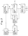
- Figure 3 is a schematic block diagram of a half-tone image processing system according to a first embodiment of the present invention.
- reference number 1 denotes a density data memory
- 2 a Laplacian calculation unit
- 3 a binary-coding unit
- 4 an error calculation unit
- 5 an error distribution unit
- 6 a binary data output unit.
- TH1 denotes a threshold value for binary-coding.
- the threshold value TH1 is preset as a fixed value.
- the corrected data DA for the object pixel is applied to the binary-coding unit 3 and the error calculation unit 4, and compared with the threshold value TH1.
- the binary-coding unit 3 when the corrected object pixel data DA is equal to or larger than the threshold value TH1, the binary-coding unit 3 outputs the bit "1".
- binary-coding unit 3 When the corrected data DA is smaller than the threshold value TH1, binary-coding unit 3 outputs the bit "0".
- the error calculation unit 4 calculates the binary-coded error ER between the corrected data DA and the output of the binary-coding unit 3. In this case, when the output of the binary-coding unit 3 is the bit "1", the maximum value of the density data is input to the error calculation unit 4. When the output of the binary-coding unit 3 is the bit "0", the minimum value of the density data is input to the error calculation unit 4.
- the error ER is output from the error calculation unit 4 to the error distribution unit 5.
- the error distribution unit 5 distributes the binary-coded error ER to density data of the peripheral pixel (the pixel to be processed) based on the error diffusion coefficient, and adds the distributed error value to the corresponding original pixel to revise the density data of the original pixel.
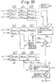
- Figure 4 is a block diagram of the half-tone image processing system shown in Fig. 3
- Figure 5 is a partially detailed block diagram of the half-tone image processing system shown in Fig. 3
- Figure 6 is a detailed block diagram of the Laplacian calculation unit shown in Fig. 3
- Figure 7 is a detailed block diagram of the error distribution unit shown in Fig. 3
- Figures 8A to 8C are examples of Laplacian coefficient matrixes used in the Laplacian calculation of the binary-coded error.
- reference number 11 denotes a density data line buffer (RAM) corresponding to the density data memory 1 in Fig. 3.
- Reference number 14 denotes an adder corresponding to the error calculation unit 4 in Fig. 3.
- Reference number 17 also denotes an adder included in the error distribution unit 5 in Fig. 3.
- Reference number 18 denotes an error diffusion matrix.
- the original image is read out by a line-type image sensor (not shown) having N (integer) sensing elements for every line, and is digitized in accordance with the density data.
- the density data of each pixel is constituted by eight bits so that it is possible to express the density data of the pixel by 256 (integer) density gradations (from 0 to 255). That is, the minimum density is the integer 0, and the maximum density is the integer 255.
- D m-1,n-1, D m-1,n, --- D m+1,n+1 represent the density data of each of the pixels. These pixels correspond to the matrix shown in Fig. 8A, and the data D m,n represents the density data of the object pixel.
- the density data of the object and the peripheral pixels are input to the Laplacian calculation unit 12. The following calculation is performed in the Laplacian calculation unit 12.
- D m,n ' D m,n + P((D m,n - D m-1,n ) + (D m,n - D m,n-1 ) + (D m,n - D m,n+1 ) + (D m,n - D m+1,n ))
- P is a positive value.
- the Laplacian calculation is performed for the difference between the object pixel (m,n) and the peripheral pixels (m-1,n; m,n-1; m,n+1; m+1,n) around the object pixel.
- the corrected data (modified object pixel data item) D m,n ' is input to the binary-coding unit 13, and is compared with the preset threshold value TH1.
- the binary-coded density data (O m,n ) of the object pixel (m,n) is expressed by the value 255 (black).
- the binary-coded density data (O m,n ) of the object pixel D m,n is expressed by the value 0 (white).
- the binary-coded data O m,n is than output from the binary-data output unit 16. That is, when the data O m,n is "255", the output value is the bit "1" (black), and when the data O m,n is "O”, the output value is the bit "O” (white).
- the binary-coded data O m,n is also output from the binary-coded unit 13 to the adder 14.
- the binary-coded error E m,n is obtained as the difference between the corrected data D m,n ' and the binary-coded data O m,n as shown by the following formula.
- E m.n D m,n ' - O m,n
- the binary-coded error E m.n is input to the error distribution unit 15, is weighted by the error diffusion coefficient K, and is distributed to the peripheral pixels (m,n+1; m+1,n-1; m+1,n; m+1,n+1) in accordance with the error diffusion matrix 18. Accordingly, the density data of the peripheral pixels (m,n+1: m+1,n-1; m+1,n; m+1,n+1) are corrected as follows.
- the binary-coded error E m,n is used for obtaining the corrected density data of the peripheral pixels.
- Figure 5 is a partially detailed block diagram of the half-tone image processing system of Fig. 3
- Figure 6 is a detailed block diagram of the Laplacian calculation unit of Fig. 3
- Figure 7 is a detailed block diagram of the error distribution unit of Fig. 3.
- each density data line buffer is constituted by a RAM functioning as a FIFO (first-in first-out) buffer.
- Reference numbers 33 to 40 denote latch circuits for storing the data
- 41 to 44 denote adders
- 45 denotes a Laplacian calculation unit corresponding to the Laplacian calculation unit 12 in Fig. 4
- 46 denotes an error distribution unit corresponding to the error distribution unit 15 in Fig. 4
- 47 denotes binary-coding circuit
- 48 denotes an adder for error calculation.
- reference numbers 50 to 56, 58 denote adders
- reference number 57 denotes a conversion table.
- reference numbers 59 to 62 denote conversion tables (for example, ROM).
- the density data D m,n of the latch circuit 37 i.e., the density data of the object pixel (m,n) is input to the Laplacian calculation unit 45. Further, the density data of the peripheral pixels, i.e., the density data D m-1,n of the latch circuit 40, the density data D m,n-1 of the latch circuit 38, the density data D m,n+1 of the latch circuit 36, and the density data D m+1,n of the latch circuit 34 are also input to the Laplacian calculation unit 45.
- the density data D m,n is added to each density data D m-1,n , D m,n-1 , D m,n+1 and D m+1,n by using each of the adders 50 to 56 as shown in Fig. 6.
- the resultant data of the adder 56 is input to the conversion table 57.
- the conversion table 57 previously stores the resultant data from multiplying the Laplacian coefficient by the density data.
- the adder 58 adds the density data D m,n of the object pixel (m,n) to the output of the conversion table 57 so that the adder 58 outputs the corrected density data D m,n '.
- the corrected density data D m,n ' is input to the binary-coding circuit 47 as shown in Fig. 5, and is compared with the threshold value TH1.
- the binary-coding circuit 47 outputs the binary data as follows.
- the binary-coded output (O m,n ) is "1"
- the density data becomes maximum (all eight bits are “1") so that all eight bits become "O” as the complement of the output "1".
- the binary-coded output (O m,n ) is "O"
- the density data becomes maximum (all eight bits are “O") so that all eight bits become “1” as the complement of the output "O”.
- the binary-coding circuit 47 is constituted by, for example, a comparator and a NOT circuit (both not shown).
- the binary-coded error E m,n is obtained by the adder 48 is based on the density data D m,n and the inverted output O m,n .
- the binary-coded error E m,n is input to the error distribution unit 46 as shown in Fig. 7.
- Each of the conversion tables 59 to 62 stores the error distribution value which is previously obtained from the weighted coefficient of the error diffusion matrix 18 shown in Fig. 4, and outputs the error distribution values (E m,n+1 , E m+1,n-1 , E m+1,n , E m+1,n+1 ). These error distribution values are input to the adders 41 to 44 as shown in Fig. 5.
- the adders 41 to 44 add the Q output of the latch circuits 33 to 36 (D m,n+1 , D m+1,n-1 , D m+1,n , D m+1,n+1 ) to the error distribution values (E m,n+1 , E m+1,n-1 , E m+1,n , E m+1,n+1 ), respectively.
- Figures 8A to 8C are examples of Laplacian coefficient matrixes used in the Laplacian calculation of the binary-coded error.
- each number denotes a Laplacian coefficient for weighting the density data as previously explained.
- the center pixel denotes an object pixel to be weighted.
- many peripheral pixels are provided around the object pixel (+36), but the Laplacian calculation is the same as shown in Fig. 8A.
- FIG. 9 is a schematic block diagram of a half-tone image processing system according to a second embodiment of the present invention.
- the same reference numbers as used in Fig. 4 are attached to the same components in this drawing.
- the structure of this embodiment is basically the same structure as that of the first embodiment shown in Fig. 4.
- the density data D m,n of the object pixel (m,n) is input to the binary-coding unit 13 and the adder 14.
- the resultant data D x (difference data item) of the Laplacian calculation is used as the threshold value TH2.
- the resultant data D X is obtained from the formula (1).
- the threshold value TH2 is variable in this embodiment.
- the density data D m,n of the object pixel (m,n) is compared with the threshold value TH2. That is, when the density data D m,n is larger than the threshold value TH2, the binary-coded density data O m,n is expressed by the value 255 (black). When the density data D m,n is equal to or smaller than the threshold value TH2, the binary-coded density data O m,n is expressed by the value O (white).
- the binary-coded density data O m,n is output to the binary-data output unit 16. That is, when the data O m,n is "255", the output value from the binary-data output unit 16 is "1" (black), and when the data O m,n is "O", the output value is "O" (white).
- the binary-coded data O m,n is also output from the binary-coding unit 13 to the adder 14.
- the binary-coded error E m.n is obtained as the difference between the density data D m,n and the binary-coded data O m,n as shown by the following formula.
- E m.n D m,n - O m,n
- the binary-coded error E m.n is input to the error distribution unit 15.
- the subsequent explanations are omitted since, after this stage, the calculations are the same as those of the first embodiment shown in Fig. 4.
- the density data D m,n , the resultant data D x , and the correction value C m,n are added to each other in the adder 22, and the adder 22 outputs the resultant data D m,n '' to the binary-coding unit 13 and the adder 14.
- the resultant data D m,n '' is compared with a threshold value TH3.
- the threshold value TH3 is preset as a fixed value.
- the binary-coded error E m,n of the formula (5) is input to the error data line buffer 20 so that the correction value C m,n can be obtained from the formula (4) in the average error calculation unit 21 as explained above.
Landscapes
- Engineering & Computer Science (AREA)
- Multimedia (AREA)
- Signal Processing (AREA)
- Physics & Mathematics (AREA)
- General Physics & Mathematics (AREA)
- Theoretical Computer Science (AREA)
- Facsimile Image Signal Circuits (AREA)
- Image Processing (AREA)
Claims (6)
- Bilddatenverarbeitungsschaltungsanordnung zum Verarbeiten von Bilddatenelementen, die für die jeweiligen Dichtewerte von Pixels, die ein Originalbild bilden, repräsentativ sind, um Ausgabedatenelemente zum Bestimmen der Dichtewerte von Pixels abzuleiten, die ein entsprechendes binäres Ausgabebild bilden, welche Schaltungsanordnung enthält:ein Speichermittel (11) zum Speichern von sukzessiven Sätzen solcher Bilddatenelemente, die sich jeweilig auf solche Originalbildpixels beziehen, von welchen Sätzen jeder gebildet ist aus einem Datenelement (Dm,n), das sich auf ein Objektpixel bezieht, und weiteren Datenelementen (Dm-1,n-1, ..., Dm+1,n+1), die sich jeweilig auf periphere Pixels beziehen, die an das genannte Objektpixel angrenzen;ein Berechnungsmittel (12), das mit dem genannten Speichermittel (11) verbunden ist und betriebsfähig ist, um Bilddatenelemente solch eines gespeicherten Satzes zu empfangen und ein abgewandeltes Objektpixeldatenelement (Dm,n') zu erzeugen, das von dem genannten Bilddatenelement (Dm,n) abgeleitet ist, das sich auf das genannte Objektpixel des Satzes bezieht, in Abhängigkeit von den jeweiligen Differenzen von Dichtewerten zwischen jenem Objektpixelbilddatenelement (Dm,n) und solch weiteren Datenelementen (Dm-1,n, Dm,n-1, Dm,n+1, Dm+1,n) des betreffenden Satzes;ein Vergleichsmittel (13), das verbunden ist, um das abgewandelte Objektpixeldatenelement (Dm,n') zu empfangen, und betriebsfähig ist, um den Dichtewert jenes Datenelementes (Dm,n') mit einem voreingestellten Schwellenwert (TH₁) zu vergleichen und um in Abhängigkeit von dem Resultat solch eines Vergleichs solch ein Ausgabedatenelement (Om,n) zu bestimmen, das dem betreffenden Objektpixel entspricht; undein Fehlerkorrekturmittel (14, 15), das betriebsfähig ist, um einen Objektpixelfehler (Em,n) zu bestimmen, der für die Differenz von Dichtewerten zwischen dem genannten abgewandelten Objektpixeldatenelement (Dm,n') und dem bestimmten Ausgabedatenelement (Om,n) repräsentativ ist, und auch betriebsfähig ist, um in Abhängigkeit von jenem Fehler (Em,n) solche weiteren Datenelemente in dem genannten Speichermittel (11) abzuwandeln, so daß die Schaltungsanordnung solch einen bestimmten Objektpixelfehler kompensieren kann, wenn ein nachfolgender Satz solcher Bilddatenelemente verarbeitet wird.
- Bilddatenverarbeitungsschaltungsanordnung zum Verarbeiten von Bilddatenelementen, die für die jeweiligen Dichtewerte von Pixels, die ein Originalbild bilden, repräsentativ sind, um Ausgabedatenelemente zum Bestimmen der Dichtewerte von Pixels abzuleiten, die ein entsprechendes binäres Ausgabebild bilden, welche Schaltungsanordnung enthält:ein Speichermittel (11) zum Speichern von sukzessiven Sätzen solcher Bilddatenelemente, die sich jeweilig auf solche Originalbildpixels beziehen, von welchen Sätzen jeder gebildet ist aus einem Datenelement (Dm,n), das sich auf ein Objektpixel bezieht, und weiteren Datenelementen (Dm-1,n-1, ... Dm+1,n+1), die sich jeweilig auf periphere Pixels beziehen, die an das genannte Objektpixel angrenzen;ein Berechnungsmittel (12), das mit dem genannten Speichermittel (11) verbunden ist und betriebsfähig ist, um Bilddatenelemente solch eines gespeicherten Satzes zu empfangen und um ein Differenzdatenelement (Dx) in Abhängigkeit von den jeweiligen Differenzen von Dichtewerten zwischen dem Objektpixeldatenelement (Dm,n) des Satzes und solch weiteren Datenelementen (Dm-1,n, Dm,n-1, Dm,n+1, Dm+1,n) des betreffenden Satzes zu erzeugen;ein Vergleichsmittel (13), das verbunden ist, um das genannte Bilddatenelement (Dm,n), das sich auf das genannte Objektpixel bezieht, und das genannte Differenzdatenelement (Dx) zu empfangen, und betriebsfähig ist, um die jeweiligen Dichtewerte jener Datenelemente (Dm,n, Dx) zu vergleichen und um in Abhängigkeit von dem Resultat solch eines Vergleichs solch ein Ausgabedatenelement (Om,n) zu bestimmen, das dem betreffenden Objektpixel entspricht; undein Fehlerkorrekturmittel (14, 15), das betriebsfähig ist, um einen Objektpixelfehler (Em,n) zu bestimmen, der für die Differenz von Dichtewerten zwischen dem genannten Bilddatenelement (Dm,n), das sich auf das genannte Objektpixel bezieht, und dem bestimmten Ausgabedatenelement (Om,n) repräsentativ ist, und auch betriebsfähig ist, um in Abhängigkeit von jenem Fehler (Em,n) solche weiteren Datenelemente in dem genannten Speichermittel (11) abzuwandeln, so daß die Schaltungsanordnung solch einen bestimmten Objektpixelfehler kompensieren kann, wenn ein nachfolgender Satz solcher Bilddatenelemente verarbeitet wird.
- Bilddatenverarbeitungsschaltungsanordnung nach Anspruch 1 oder 2, bei der das genannte Fehlerkorrekturmittel (14, 15) eine Fehlerverteileinheit (15) enthält, die zum Empfangen des bestimmten Objektpixelfehlers (Em,n) verbunden ist und auch zum Empfangen einer vorbestimmten Fehlerdiffusionsmatrix (K) verbunden ist, und betriebsfähig ist, um für jedes periphere Pixel des genannten Satzes, das dem genannten Objektpixel folgt, einen gewichteten Fehlerwert (zum Beispiel Km-1,n-1 x Em,n) zu berechnen, auf der Basis des bestimmten Objektpixelfehlers (Em,n) und Wichtungswertes (zum Beispiel Km-1,n-1) in der genannten Fehlerdiffusionsmatrix (K), der jenem peripheren Pixel entspricht;welche Schaltungsanordnung ferner ein Datenelementabwandlungsmittel (17) enthält, das mit dem genannten Fehlerkorrekturmittel (14, 15) verbunden ist, zum Empfangen von diesem der jeweiligen gewichteten Fehlerwerte für die peripheren Pixels, die dem Objektpixel folgen, und betriebsfähig ist, um die weiteren Datenelemente, die sich auf jene Pixels beziehen, jeweilig in Abhängigkeit von den gewichteten Fehlerwerten abzuwandeln.
- Bilddatenverarbeitungsschaltungsanordnung zum Verarbeiten von Bilddatenelementen, die für die jeweiligen Dichtewerte von Pixels, die ein Originalbild bilden, repräsentativ sind, um Ausgabedatenelemente zum Bestimmen der Dichtewerte von Pixels abzuleiten, die ein entsprechendes binäres Ausgabebild bilden, welche Schaltungsanordnung enthält:ein Speichermittel (11) zum Speichern von sukzessiven Sätzen solcher Bilddatenelemente, die sich jeweilig auf solche Originalbildpixels beziehen, von welchen Sätzen jeder gebildet ist aus einem Datenelement (Dm,n), das sich auf ein Objektpixel bezieht, und weiteren Datenelementen (Dm-1,n-1, ... Dm+1,n+1), die sich jeweilig auf periphere Pixels beziehen, die an das genannte Objektpixel angrenzen;ein Berechnungsmittel (12, 22), das mit dem genannten Speichermittel (11) verbunden ist und betriebsfähig ist, um Bilddatenelemente von solch einem gespeicherten Satz zu empfangen und um ein abgewandeltes Objektpixeldatenelement (Dm,n") zu erzeugen, das von dem genannten Bilddatenelement (Dm,n) abgeleitet ist, das sich auf das genannte Objektpixel des Satzes bezieht, in Abhängigkeit von den jeweiligen Differenzen von Dichtewerten zwischen jenem Objektpixelbilddatenelement (Dm,n) und solch weiteren Datenelementen (Dm-1,n, Dm,n-1, Dm,n+1, Dm+1,n) des betreffenden Satzes und auch in Abhängigkeit von einem Korrekturwert (Cm,n) für das Objektpixel des betreffenden Satzes;ein Vergleichsmittel (13), das verbunden ist, um das abgewandelte Objektpixeldatenelement (Dm,n'') zu empfangen, und betriebsfähig ist, um den Dichtewert von jenem Datenelement (Dm,n'') mit einem voreingestellten Schwellenwert (TH₃) zu vergleichen und um in Abhängigkeit von dem Resultat solch eines Vergleichs solch ein Ausgabedatenelement (Om,n) zu bestimmen, das dem betreffenden Objektpixel entspricht; undein Fehlerkorrekturmittel (14, 19-21), das betriebsfähig ist, um einen Objektpixelfehler (Em,n) zu bestimmen, der für die Differenz von Dichtewerten zwischen dem genannten abgewandelten Objektpixeldatenelement (Dm,n'') und dem bestimmten Ausgabedatenelement (Om,n) repräsentativ ist, und auch betriebsfähig ist, um jenen Fehler zur Verwendung durch die Schaltungsanordnung beim Berechnen des Korrekturwertes für das Objektpixel eines nachfolgenden Satzes solcher Bilddatenelemente zu speichern, so daß die Schaltungsanordnung dadurch solch einen bestimmten Objektpixelfehler kompensieren kann, wenn jener nachfolgende Satz verarbeitet wird.
- Bilddatenverarbeitungsschaltungsanordnung zum Verarbeiten von Bilddatenelementen, die für die jeweiligen Dichtewerte von Pixels, die ein Originalbild bilden, repräsentativ sind, um Ausgabedatenelemente zum Bestimmen der Dichtewerte von Pixels abzuleiten, die ein entsprechendes binäres Ausgabebild bilden, welche Schaltungsanordnung enthält:ein Speichermittel (11) zum Speichern von sukzessiven Sätzen solcher Bilddatenelemente, die sich jeweilig auf solche Originalbildpixels beziehen, von welchen Sätzen jeder gebildet ist aus einem Datenelement (Dm,n), das sich auf ein Objektpixel bezieht, und weiteren Datenelementen (Dm-1,n- 1, ..., Dm+1, n+1), die sich jeweilig auf periphere Pixels beziehen, die an das genannte Objektpixel angrenzen;ein Berechnungsmittel (12, 22), das mit dem genannten Speichermittel (11) verbunden ist und betriebsfähig ist, um Bilddatenelemente solch eines gespeicherten Satzes zu empfangen und um ein Differenzdatenelement (Dx) in Abhängigkeit von den jeweiligen Differenzen von Dichtewerten zwischen dem Objektpixelbilddatenelement (Dm,n) des Satzes und solch weiteren Datenelementen des betreffenden Satzes zu erzeugen, und auch betriebsfähig ist, um ein korrigiertes Objektpixeldatenelement (Dm,n'''), das von dem genannten Objektpixeldatenelement (Dm,n) abgeleitet ist, in Abhängigkeit von einem Korrekturwert (Cm,n) für jenes Objektpixel zu erzeugen;ein Vergleichsmittel (13), das verbunden ist, um das genannte korrigierte Objektpixeldatenelement (Dm,n''') und das genannte Differenzdatenelement (Dx) zu empfangen, und betriebsfähig ist, um die jeweiligen Dichtewerte von jenen Datenelementen (Dm,n''', Dx) zu vergleichen und um in Abhängigkeit von dem Resultat solch eines Vergleichs solch ein Ausgabedatenelement (Om,n) zu bestimmen, das dem betreffenden Objektpixel entspricht; undein Fehlerkorrekturmittel (14, 15), das betriebsfähig ist, um einen Objektpixelfehler (Em,n) zu bestimmen, der für die Differenz von Dichtewerten zwischen dem genannten korrigierten Objektpixeldatenelement (Dm,n''') und dem bestimmten Ausgabedatenelement (Om,n) repräsentativ ist, und auch betriebsfähig ist, um jenen Fehler zur Verwendung durch die Schaltungsanordnung beim Berechnen des Korrekturwertes für das Objektpixel eines nachfolgenden Satzes solcher Bilddatenelemente zu speichern, so daß die Schaltungsanordnung dadurch solch einen bestimmten Objektpixelfehler kompensieren kann, wenn jener nachfolgende Satz verarbeitet wird.
- Bilddatenverarbeitungsschaltungsanordnung nach Anspruch 4 oder 5, bei der das genannte Fehlerkorrekturmittel (14, 19-21) betriebsfähig ist, um für jedes periphere Pixel des genannten Satzes, das dem genannten Objektpixel vorausgeht, den Objektpixelfehler (Em-1,n-1, Em-1,n, Em-1,n+1, Em,n-1) wiederaufzufinden, der durch das Fehlerkorrekturmittel beim Verarbeiten eines vorhergehenden Satzes der Bilddatenelemente, der als sein genanntes Objektpixel das betreffende periphere Pixel hatte, gespeichert wurde;welches Fehlerkorrekturmittel eine Durchschnittsfehlerberechnungseinheit enthält, die zum Empfangen einer vorbestimmten fehlergewichteten Matrix (K) verbunden ist und betriebsfähig ist, um die wiederaufgefundenen Fehler in Abhängigkeit von jeweiligen entsprechenden Wichtungswerten in der genannten fehlergewichteten Matrix (K) zu kombinieren, um den genannten Korrekturwert (Cm,n) zu berechnen.
Applications Claiming Priority (8)
| Application Number | Priority Date | Filing Date | Title |
|---|---|---|---|
| JP111320/90 | 1990-04-26 | ||
| JP2111320A JPH048063A (ja) | 1990-04-26 | 1990-04-26 | 画像処理方式 |
| JP2130701A JPH0426277A (ja) | 1990-05-21 | 1990-05-21 | 画像処理方法 |
| JP130701/90 | 1990-05-21 | ||
| JP2133847A JPH0435163A (ja) | 1990-05-25 | 1990-05-25 | 画像処理装置 |
| JP133851/90 | 1990-05-25 | ||
| JP133847/90 | 1990-05-25 | ||
| JP2133851A JPH0435166A (ja) | 1990-05-25 | 1990-05-25 | 画像処理装置 |
Publications (2)
| Publication Number | Publication Date |
|---|---|
| EP0454495A1 EP0454495A1 (de) | 1991-10-30 |
| EP0454495B1 true EP0454495B1 (de) | 1996-02-07 |
Family
ID=27469897
Family Applications (1)
| Application Number | Title | Priority Date | Filing Date |
|---|---|---|---|
| EP91303820A Expired - Lifetime EP0454495B1 (de) | 1990-04-26 | 1991-04-26 | Halbton-Bildverarbeitungssystem |
Country Status (4)
| Country | Link |
|---|---|
| US (1) | US5208684A (de) |
| EP (1) | EP0454495B1 (de) |
| KR (1) | KR950006440B1 (de) |
| DE (1) | DE69116924T2 (de) |
Cited By (5)
| Publication number | Priority date | Publication date | Assignee | Title |
|---|---|---|---|---|
| US7826660B2 (en) | 2003-02-27 | 2010-11-02 | Saquib Suhail S | Digital image exposure correction |
| US7907157B2 (en) | 2002-02-19 | 2011-03-15 | Senshin Capital, Llc | Technique for printing a color image |
| USRE42473E1 (en) | 2001-05-30 | 2011-06-21 | Senshin Capital, Llc | Rendering images utilizing adaptive error diffusion |
| USRE43149E1 (en) | 2001-03-27 | 2012-01-31 | Senshin Capital, Llc | Method for generating a halftone of a source image |
| US8773685B2 (en) | 2003-07-01 | 2014-07-08 | Intellectual Ventures I Llc | High-speed digital image printing system |
Families Citing this family (15)
| Publication number | Priority date | Publication date | Assignee | Title |
|---|---|---|---|---|
| JPH0583556A (ja) * | 1991-09-18 | 1993-04-02 | Konica Corp | 画像処理装置 |
| US5917614A (en) * | 1992-11-30 | 1999-06-29 | Levien; Raphael L | Method and apparatus for error diffusion screening of images with improved smoothness in highlight and shadow regions |
| US5625755A (en) * | 1994-07-01 | 1997-04-29 | Seiko Epson Corporation | Method and apparatus for tonal correction in binary printing devices by predistortion of image data utilizing ink reduction processing |
| US5568572A (en) * | 1994-07-01 | 1996-10-22 | Seiko Epson Corporation | Method and apparatus for tonal correction in binary printing devices by predistortion of image data |
| JP3381755B2 (ja) * | 1994-10-11 | 2003-03-04 | セイコーエプソン株式会社 | 画像の粒状性を減らすための改良された適応性のあるフィルタリングおよび閾値設定の方法及び装置 |
| US5870503A (en) * | 1994-10-20 | 1999-02-09 | Minolta Co., Ltd. | Image processing apparatus using error diffusion technique |
| US5757517A (en) * | 1995-03-23 | 1998-05-26 | Eastman Kodak Company | Adaptive error diffusion method |
| US5668638A (en) * | 1996-06-27 | 1997-09-16 | Xerox Corporation | Error diffusion method with symmetric enhancement |
| JP3397059B2 (ja) * | 1996-11-07 | 2003-04-14 | セイコーエプソン株式会社 | 印刷装置および画像記録方法 |
| KR100251551B1 (ko) * | 1997-03-06 | 2000-04-15 | 구자홍 | 디지탈영상양자화를위한비인과성오차확산계수의위치및결정방법 |
| JP4404457B2 (ja) * | 2000-07-21 | 2010-01-27 | 富士通株式会社 | ハーフトーン化方法およびハーフトーン化装置並びにハーフトーン化プログラムを記録したコンピュータ読み取り可能な記録媒体 |
| JP3983101B2 (ja) * | 2001-05-25 | 2007-09-26 | 株式会社リコー | 画像処理装置、画像読み取り装置、画像形成装置およびカラー複写装置 |
| JP5254740B2 (ja) * | 2008-10-24 | 2013-08-07 | キヤノン株式会社 | 画像処理装置および画像処理方法 |
| JP5254739B2 (ja) * | 2008-10-24 | 2013-08-07 | キヤノン株式会社 | 画像形成装置およびその制御方法 |
| JP5241429B2 (ja) * | 2008-10-24 | 2013-07-17 | キヤノン株式会社 | 画像形成装置およびその制御方法 |
Family Cites Families (11)
| Publication number | Priority date | Publication date | Assignee | Title |
|---|---|---|---|---|
| JPS6074091A (ja) * | 1983-09-30 | 1985-04-26 | Fujitsu Ltd | 2値化回路 |
| US4654722A (en) * | 1985-05-06 | 1987-03-31 | Eastman Kodak Company | Tone value sample selection in digital image processing method employing histogram normalization |
| US5029227A (en) * | 1985-08-30 | 1991-07-02 | Canon Kabushiki Kaisha | Image processing apparatus |
| US4764971A (en) * | 1985-11-25 | 1988-08-16 | Eastman Kodak Company | Image processing method including image segmentation |
| JPS62239666A (ja) * | 1986-04-10 | 1987-10-20 | Seiko Epson Corp | 2値化処理装置 |
| US5109430A (en) * | 1986-07-22 | 1992-04-28 | Schlumberger Technologies, Inc. | Mask alignment and measurement of critical dimensions in integrated circuits |
| JPS63155273A (ja) * | 1986-12-18 | 1988-06-28 | Fujitsu Ltd | 画像処理装置 |
| JPS63204375A (ja) * | 1987-02-19 | 1988-08-24 | Fuji Xerox Co Ltd | 中間調画像生成方法 |
| US4797942A (en) * | 1987-03-02 | 1989-01-10 | General Electric | Pyramid processor for building large-area, high-resolution image by parts |
| JP2701310B2 (ja) * | 1988-04-18 | 1998-01-21 | 富士ゼロックス株式会社 | 中間調画像生成方法および装置 |
| US5113365A (en) * | 1989-05-16 | 1992-05-12 | Massachusetts Institute Of Technology | Method and charge coupled apparatus for algorithmic computations |
-
1991
- 1991-04-24 US US07/690,574 patent/US5208684A/en not_active Expired - Fee Related
- 1991-04-26 KR KR1019910006752A patent/KR950006440B1/ko not_active Expired - Fee Related
- 1991-04-26 DE DE69116924T patent/DE69116924T2/de not_active Expired - Fee Related
- 1991-04-26 EP EP91303820A patent/EP0454495B1/de not_active Expired - Lifetime
Cited By (6)
| Publication number | Priority date | Publication date | Assignee | Title |
|---|---|---|---|---|
| USRE43149E1 (en) | 2001-03-27 | 2012-01-31 | Senshin Capital, Llc | Method for generating a halftone of a source image |
| USRE42473E1 (en) | 2001-05-30 | 2011-06-21 | Senshin Capital, Llc | Rendering images utilizing adaptive error diffusion |
| US7907157B2 (en) | 2002-02-19 | 2011-03-15 | Senshin Capital, Llc | Technique for printing a color image |
| US7826660B2 (en) | 2003-02-27 | 2010-11-02 | Saquib Suhail S | Digital image exposure correction |
| US8265420B2 (en) | 2003-02-27 | 2012-09-11 | Senshin Capital, Llc | Digital image exposure correction |
| US8773685B2 (en) | 2003-07-01 | 2014-07-08 | Intellectual Ventures I Llc | High-speed digital image printing system |
Also Published As
| Publication number | Publication date |
|---|---|
| DE69116924D1 (de) | 1996-03-21 |
| DE69116924T2 (de) | 1996-06-20 |
| KR910018861A (ko) | 1991-11-30 |
| US5208684A (en) | 1993-05-04 |
| EP0454495A1 (de) | 1991-10-30 |
| KR950006440B1 (ko) | 1995-06-15 |
Similar Documents
| Publication | Publication Date | Title |
|---|---|---|
| EP0454495B1 (de) | Halbton-Bildverarbeitungssystem | |
| EP0356225B1 (de) | Bildverarbeitungsgerät | |
| EP0659012B1 (de) | Verfahren zur Quantisierung von Grautonbilddaten mit erweitertem Verteilungssatz | |
| KR960014303B1 (ko) | 화상 처리 장치 | |
| US5394250A (en) | Image processing capable of handling multi-level image data without deterioration of image quality in highlight areas | |
| EP0591274B1 (de) | Verbessertes fehler-diffusionssystem | |
| US5289294A (en) | Image processing apparatus | |
| JP4248654B2 (ja) | 出力装置へ出力する文書イメージを準備する処理装置 | |
| US5760918A (en) | Image processing apparatus with conversion and reconversion of the number of bits per pixel | |
| EP0382580B1 (de) | Bildverarbeitungsgerät | |
| EP0786741B1 (de) | Verfahren und Vorrichtung zur Binärkodierung von Bilddaten | |
| US6134355A (en) | Binarization using a local average, and using error diffusion | |
| US5825509A (en) | Image processing device with error-diffusion quantization function | |
| US5200839A (en) | Image processing apparatus | |
| JP3197299B2 (ja) | 画像処理装置 | |
| JPH05183737A (ja) | 画像処理装置 | |
| JP3124589B2 (ja) | 画像処理装置 | |
| JP2703911B2 (ja) | 画像処理装置 | |
| JP3142699B2 (ja) | 画像処理装置 | |
| JP3974271B2 (ja) | 画像処理方法及び画像処理装置 | |
| KR100440944B1 (ko) | 이진화상의 해상도를 축소시키는 방법 및 장치 | |
| EP0481808A2 (de) | Bildverarbeitungsvorrichtung und Verfahren | |
| JP2504347B2 (ja) | 中間調画像処理装置 | |
| JPH0426277A (ja) | 画像処理方法 | |
| JP2000050067A (ja) | 画像処理方法及びその装置 |
Legal Events
| Date | Code | Title | Description |
|---|---|---|---|
| PUAI | Public reference made under article 153(3) epc to a published international application that has entered the european phase |
Free format text: ORIGINAL CODE: 0009012 |
|
| AK | Designated contracting states |
Kind code of ref document: A1 Designated state(s): DE FR GB |
|
| 17P | Request for examination filed |
Effective date: 19911209 |
|
| 17Q | First examination report despatched |
Effective date: 19940317 |
|
| GRAA | (expected) grant |
Free format text: ORIGINAL CODE: 0009210 |
|
| AK | Designated contracting states |
Kind code of ref document: B1 Designated state(s): DE FR GB |
|
| PGFP | Annual fee paid to national office [announced via postgrant information from national office to epo] |
Ref country code: FR Payment date: 19960214 Year of fee payment: 6 |
|
| REF | Corresponds to: |
Ref document number: 69116924 Country of ref document: DE Date of ref document: 19960321 |
|
| PGFP | Annual fee paid to national office [announced via postgrant information from national office to epo] |
Ref country code: GB Payment date: 19960419 Year of fee payment: 6 |
|
| ET | Fr: translation filed | ||
| PGFP | Annual fee paid to national office [announced via postgrant information from national office to epo] |
Ref country code: DE Payment date: 19960622 Year of fee payment: 6 |
|
| PLBE | No opposition filed within time limit |
Free format text: ORIGINAL CODE: 0009261 |
|
| STAA | Information on the status of an ep patent application or granted ep patent |
Free format text: STATUS: NO OPPOSITION FILED WITHIN TIME LIMIT |
|
| 26N | No opposition filed | ||
| PG25 | Lapsed in a contracting state [announced via postgrant information from national office to epo] |
Ref country code: GB Effective date: 19970426 |
|
| GBPC | Gb: european patent ceased through non-payment of renewal fee |
Effective date: 19970426 |
|
| PG25 | Lapsed in a contracting state [announced via postgrant information from national office to epo] |
Ref country code: FR Free format text: LAPSE BECAUSE OF NON-PAYMENT OF DUE FEES Effective date: 19971231 |
|
| PG25 | Lapsed in a contracting state [announced via postgrant information from national office to epo] |
Ref country code: DE Free format text: LAPSE BECAUSE OF NON-PAYMENT OF DUE FEES Effective date: 19980101 |
|
| REG | Reference to a national code |
Ref country code: FR Ref legal event code: ST |