EP0455220A2 - Appareil de détection d'image - Google Patents
Appareil de détection d'image Download PDFInfo
- Publication number
- EP0455220A2 EP0455220A2 EP91107015A EP91107015A EP0455220A2 EP 0455220 A2 EP0455220 A2 EP 0455220A2 EP 91107015 A EP91107015 A EP 91107015A EP 91107015 A EP91107015 A EP 91107015A EP 0455220 A2 EP0455220 A2 EP 0455220A2
- Authority
- EP
- European Patent Office
- Prior art keywords
- image sensing
- sensing apparatus
- negative
- inverting
- color
- Prior art date
- Legal status (The legal status is an assumption and is not a legal conclusion. Google has not performed a legal analysis and makes no representation as to the accuracy of the status listed.)
- Granted
Links
Images


Classifications
-
- H—ELECTRICITY
- H04—ELECTRIC COMMUNICATION TECHNIQUE
- H04N—PICTORIAL COMMUNICATION, e.g. TELEVISION
- H04N1/00—Scanning, transmission or reproduction of documents or the like, e.g. facsimile transmission; Details thereof
- H04N1/46—Colour picture communication systems
- H04N1/56—Processing of colour picture signals
- H04N1/60—Colour correction or control
- H04N1/6027—Correction or control of colour gradation or colour contrast
-
- H—ELECTRICITY
- H04—ELECTRIC COMMUNICATION TECHNIQUE
- H04N—PICTORIAL COMMUNICATION, e.g. TELEVISION
- H04N1/00—Scanning, transmission or reproduction of documents or the like, e.g. facsimile transmission; Details thereof
- H04N1/40—Picture signal circuits
- H04N1/407—Control or modification of tonal gradation or of extreme levels, e.g. background level
- H04N1/4072—Control or modification of tonal gradation or of extreme levels, e.g. background level dependent on the contents of the original
-
- H—ELECTRICITY
- H04—ELECTRIC COMMUNICATION TECHNIQUE
- H04N—PICTORIAL COMMUNICATION, e.g. TELEVISION
- H04N1/00—Scanning, transmission or reproduction of documents or the like, e.g. facsimile transmission; Details thereof
- H04N1/46—Colour picture communication systems
- H04N1/56—Processing of colour picture signals
- H04N1/60—Colour correction or control
-
- H—ELECTRICITY
- H04—ELECTRIC COMMUNICATION TECHNIQUE
- H04N—PICTORIAL COMMUNICATION, e.g. TELEVISION
- H04N23/00—Cameras or camera modules comprising electronic image sensors; Control thereof
- H04N23/80—Camera processing pipelines; Components thereof
- H04N23/84—Camera processing pipelines; Components thereof for processing colour signals
- H04N23/87—Camera processing pipelines; Components thereof for processing colour signals for reinsertion of DC or slowly varying components of colour signals
-
- H—ELECTRICITY
- H04—ELECTRIC COMMUNICATION TECHNIQUE
- H04N—PICTORIAL COMMUNICATION, e.g. TELEVISION
- H04N23/00—Cameras or camera modules comprising electronic image sensors; Control thereof
- H04N23/80—Camera processing pipelines; Components thereof
- H04N23/84—Camera processing pipelines; Components thereof for processing colour signals
- H04N23/88—Camera processing pipelines; Components thereof for processing colour signals for colour balance, e.g. white-balance circuits or colour temperature control
-
- H—ELECTRICITY
- H04—ELECTRIC COMMUNICATION TECHNIQUE
- H04N—PICTORIAL COMMUNICATION, e.g. TELEVISION
- H04N5/00—Details of television systems
- H04N5/14—Picture signal circuitry for video frequency region
- H04N5/16—Circuitry for reinsertion of DC and slowly varying components of signal; Circuitry for preservation of black or white level
- H04N5/18—Circuitry for reinsertion of DC and slowly varying components of signal; Circuitry for preservation of black or white level by means of "clamp" circuit operated by switching circuit
- H04N5/185—Circuitry for reinsertion of DC and slowly varying components of signal; Circuitry for preservation of black or white level by means of "clamp" circuit operated by switching circuit for the black level
-
- H—ELECTRICITY
- H04—ELECTRIC COMMUNICATION TECHNIQUE
- H04N—PICTORIAL COMMUNICATION, e.g. TELEVISION
- H04N5/00—Details of television systems
- H04N5/222—Studio circuitry; Studio devices; Studio equipment
- H04N5/253—Picture signal generating by scanning motion picture films or slide opaques, e.g. for telecine
Definitions
- the present invention relates to an image sensing apparatus including polarity inverting means for inverting the polarity of a sensed image.
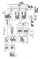
- Fig. 1 is a block diagram showing a conventional image sensing apparatus
- the apparatus includes an image sensor 1 for converting an optical image of a subject or a negative image formed on a negative film into an electrical signal, a luminance signal processing circuit 2 for processing an output signal from the image sensor 1 and producing a luminance signal Y H , and a color signal processing circuit 3 for producing RGB signals.
- the conventional image sensing apparatus also includes gain control circuits 4 and 5 for white-balance control of the respective R and B signals, a potentiometer part 6 for white-balance control which includes potentiometers independently provided for the R and B signals, a matrix circuit 7 for producing color-difference signals R-YL and B-YL, a negative/positive inversion processing circuit 8 for the luminance signal which includes circuit elements such as an inverting circuit and a blanking processing circuit for setting a pedestal level, a potentiometer 9 for setting the pedestal level, negative/positive inversion processing circuits 10 and 11 for the color-difference signals, each of which includes an inverting circuit and so on, a switching circuit 12 which is switched in accordance with a negative/positive switching control signal, and an encoder circuit 13 for generating a composite video signal from the luminance signal and the color-difference signals.
- gain control circuits 4 and 5 for white-balance control of the respective R and B signals
- Fig. 3 is a graph showing the relation between the exposure amount log H which is given to the film during photography and the relative value of a luminance signal level if the quantity of light incident on the image sensor 1 is set to a predetermined value, a luminance signal level obtained at the base portion of the film being set to 100%. If a maximum exposure amount, an average exposure amount and a minimum exposure amount are, for example, E0, E1 and E2 for the film, corresponding luminance signal levels are V E0 , V E1 and V E2 . In the conventional example, the quantity of light incident on the image sensor 1 has been adjusted so that V E2 reaches 100% or V E1 reaches a predetermined proper value (for example, 50%).
- Another object of the present invention is to provide an image sensing apparatus having an inverting function which makes it possible to provide correct exposure control over an image sensor.
- an image sensing apparatus including image sensing means, inverting means for inverting a polarity of an output of the image sensing means, and correcting means for correcting a black reference level of the output of the image sensing means in accordance with an operation of the inverting means.
- Another object of the present invention is to provide an image sensing apparatus having inversion processing means which makes it possible to highly accurately adjust white balance for any density area of a negative film.
- an image sensing apparatus including color image sensing means for converting an optical image into an electrical signal and generating a plurality of color signals, inversion processing means for inverting colors carried by the plurality of color signals, respectively, and black-level shifting means for shifting black levels of the respective color signals by a predetermined amount in accordance with an operation of the inversion processing means.
- the black levels of the plurality of color signals are shifted by the black-level shifting means during the operation of the inversion processing means.
- Another object of the present invention is to provide an image sensing apparatus which can automatically perform white-balance adjustment even if it is impossible to manually perform white-balance adjustment while viewing an image.
- an image sensing apparatus including image sensing means for converting subject light into an electrical signal and outputting a plurality of color signals, first light source color detecting means for detecting a color of a source light by means of an external circuit, negative/positive inverting means, mode selecting means for selecting a negative/positive inversion mode, and controlling means for controlling a white-balance adjusting operation of white-balance adjusting means on the basis of a predetermined value if the negative/positive inversion mode is selected by the mode selecting means.
- an image sensing apparatus which is arranged so that the predetermined value referred to in the above-described aspect can be switched from one value to another according to the kind of negative film.
- an image sensing apparatus including image sensing means for converting subject light into an electrical signal and outputting a plurality of color signals, second light source color detecting means for detecting a color of source light from an output of the image sensing means, negative/positive inverting means, and mode selecting means for selecting a negative/positive inversion mode, a white-balance adjusting operation of white-balance adjusting means being controlled by means of the second light source color detecting means if the negative/positive inversion mode is selected by the mode selecting means.
- an image sensing apparatus which is arranged to correct a predetermined value such as that referred to in the above-described embodiment on the basis of a detection value provided by the second light source color detecting means if a white-balance adjusting operation of the white-balance adjusting means is to be controlled on the basis of the predetermined value.
- an image sensing apparatus which is arranged so that predetermined values for white-balance control are switched from one value to another according to the kind of negative film on the basis of a detection value provided by the second light source color detecting means if the negative/positive inversion mode is selected by the mode selecting means referred to in the above-described aspect.
- the image sensing means converts a subject image into an electrical signal and outputs a plurality of color signals
- the first light source color detecting means detects a color of source light by means of the external circuit.
- the negative/positive inverting means effects negative/positive inversion
- the mode selecting means selects the negative/positive inversion mode. If the negative/positive inversion mode is selected by the mode selecting means, the white-balance adjusting operation of the white-balance adjusting means is controlled by the control means on the basis of the predetermined value.
- the image sensing apparatus is arranged to switch the predetermined value referred to in the above-described embodiment from one value to another according to the kind of negative film.
- the image sensing means converts subject light into an electrical signal and outputs a plurality of color signals
- the second light source color detecting means detects a color of a source light from an output of the image sensing means.
- the negative/positive inverting means effects negative/positive inversion
- the mode selecting means selects the negative/positive inversion mode. If the negative/positive inversion mode is selected by the mode selecting means, a white-balance adjusting operation of the white-balance adjusting means is controlled by means of the second light source color detecting means.
- the image sensing apparatus is arranged to correct the predetermined value on the basis of a detection value provided by the second light source color detecting means if the white-balance adjusting operation of the white-balance adjusting means is to be controlled on the basis of such a predetermined value.
- the image sensing apparatus is arranged so that the predetermined values for white-balance control are switched from one value to another according to the kind of negative film on the basis of a detection value provided by the second light source color detecting means if the negative/positive inversion mode is selected by the mode selecting means referred to in the above-described aspect.
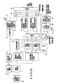
- Fig. 4 is a block diagram showing an image sensing apparatus according to a first embodiment of the present invention.
- Fig. 5 is a graph showing the relation between an exposure amount and the relative value of a luminance signal level, and serves to illustrate the first embodiment of the present invention.
- a clamping circuit 14 sets the black level of a luminance signal, and a selecting switch 15 switches the clamping potential of the clamping circuit 14 in interlocked relation to a switching circuit 12.
- the selecting switch 15 performs its switching operation in accordance with a negative/positive switching control signal.
- Clamping potentials 16 and 17 constitute black-level shifting means.
- a clamping potential V ref1 is supplied to the clamping circuit 14, and color signals and a luminance signal bypass negative/positive inversion processing circuits 10, 11 and 22, respectively, and are outputted to an encoder 13.
- a clamping potential V ref2 is supplied to the clamping circuit 14.
- a detecting circuit 18 includes an average value detecting circuit, a peak value detecting circuit and so on.
- An exposure control circuit 20 controls exposure by means of a diaphragm or the like and is driven by the output of a drive circuit 19.
- Reference numerals 21 and 22 denote an amplifier and a negative/positive inversion processing circuit, respectively.
- the output of the clamping circuit 14 is obtained as a signal level V e2 equivalent to a minimum exposure amount E2 of the film, and as a signal level V e1 equivalent to an average exposure amount E1 of the film, that is to say, as a difference with respect to a signal level equivalent to the maximum exposure amount E0.
- the detecting circuit 18 uses the output luminance signal of the clamping circuit 14 to perform average-value detection or peak-value detection. Since the exposure control circuit 20 is driven in accordance with the detection output of the detecting circuit 18, it is possible to achieve optimum exposure control.
- the signal level V e2 may be controlled to be always maintained at a level equivalent to 60% in terms of the relative value of the luminance signal level, and the gain of the amplifier 21 may be set so that the signal level V e2 can reach 100% as shown by a curve Yb in Fig. 5.
- the negative/positive inversion processing circuit 22 as shown by a curve Yc in Fig. 5, the signal level equivalent to the minimum exposure amount E 2 is inverted from 100% to 0% and the signal level equivalent to the maximum exposure amount E0 from 0% to 100%, thereby setting a pedestal level.
- the first embodiment it is possible to provide accurate exposure control over an image sensor 1 in accordance with the exposure amount of a negative film, whereby it is possible to obtain a luminance signal of correct contrast after negative/positive inversion.
- Fig. 6 is a block diagram showing an cage sensing apparatus according to a second embodiment of the present invention.
- identical reference numerals are used to denote constituent elements which are identical to or correspond to those used in the conventional example shown in Fig. 1 or those used in the first embodiment shown in Fig. 4, and description is omitted for the sake of simplicity.
- a lower-peak-level detecting circuit 23 serves as black-level shifting means and detects the lowest level of a luminance signal obtained by sensing an image on a negative film.
- a peak holding circuit 24 holds a lower peak level provided by the lower-peak-level detecting circuit 23.
- a comparing circuit 25 compares the output of the peak holding circuit 24 with the clamping potential V ref1 .
- the exposure amount E0 is the maximum exposure amount of a film to be subjected to image sensing. Therefore, the lowest level of a luminance signal provided by a luminance signal processing circuit 2 is V E0 , and this level is detected by the lower-peak-level detecting circuit 23 and held by the peak holding circuit 24.
- the comparing circuit 25 compares the held value with the clamping potential V ref1 and outputs the resultant difference voltage. The difference voltage is supplied to the clamping circuit 14 to decrease the clamping potential V ref1 .
- the luminance signal outputted from the clamping circuit 14 is controlled so that its signal level equivalent to the maximum exposure amount E0 is set to 0% as shown by the curve Ya in Fig. 5, whereby it is possible to effect highly accurate detection of luminance signal levels equivalent to the average exposure amount E1 and the minimum exposure amount E2.
- each of the first and second embodiments refers to exposure control for producing a positive image from a general negative film by inversion
- the black-level shifting means is arranged in such a manner that clamping potentials which have been set in advance are selectively set by means of the selecting switch for selecting the normal mode or the negative mode, the construction of the apparatus can be simplified.
- the black-level shifting means is arranged in such a manner that the amount of black-level shift is set in accordance with the lower peak level of a luminance signal particularly when the negative mode is selected, it is possible to provide more accurate exposure control.
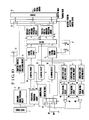
- Fig. 7 is a block diagram showing an image sensing apparatus according to the third embodiment of the present invention.
- Figs. 8 and 9 are graphs each showing the relation between an exposure amount and an output signal level, and serves to illustrate the third embodiment of the present invention.
- identical reference numerals are used to denote constituent elements which are identical to or correspond to those shown in Fig. 1, and description is omitted for the sake of simplicity.
- clamping circuits 34 to 36 set the black levels of RGB signals, respectively.
- a selecting switch 37 switches the clamping potentials of the respective clamping circuits 34 to 36 in interlocked relation to the switching circuit 12.
- the switching circuit 12 performs its switching operation in accordance with a negative/positive switching control signal.
- Clamping potentials 38 to 40 constitute black-level shifting means.
- Figs. 8 and 9 are graphs each showing the relations between the exposure amount log H and the relative values (100%: the signal level of G of a film base) of RGB color signal outputs which are respectively obtained from the outputs of the clamping circuits 34 to 36 when a negative film of characteristic shown in Fig. 2 is subjected to image sensing.
- Fig. 8 shows the case of the normal mode while
- Fig. 9 shows the case of the negative mode.
- the clamping potentials for R, G and B are V ref .
- the output signal levels of the respective RGB colors exhibit characteristics proportional to film density as shown in Fig. 8.
- the output signal levels equivalent to a certain exposure amount E0 are V R0 , V G0 and V B0 , so that an extremely large deviation occurs in white balance.
- V R is supplied as a clamping voltage for an R signal
- Gain control circuits 4 and 5 effect gain adjustment in accordance with a white-balance control potentiometer part 6 so as to reduce deviation in the white balance of a portion which shows a small exposure amount, that is, a high signal level. Accordingly, it is possible to minimize the deviation in white balance over the entire range of signal levels.
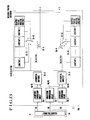
- Fig. 10 is a block diagram showing an image sensing apparatus according to a fourth embodiment of the present invention.
- identical reference numerals are used to denote constituent elements which are identical to or correspond to those of the conventional example shown in Fig. 1 or those of the third embodiment shown in Fig. 7, and description is omitted for the sake of simplicity.
- lower-peak-level detecting circuits 41 to 43 are provided as black-level shifting means, and detect the lowest levels of individual RGB signals obtained by sensing an image on a negative film.
- Peak holding circuits 44 to 46 hold lower peak levels provided by the lower-peak-level detecting circuits 41 to 43.
- a comparing circuit 47 compares the output of the peak holding circuit 44 with the output of the peak holding circuit 45, while a comparing circuit 48 compares the output of the peak holding circuit 45 with the output of the peak holding circuit 46.
- the exposure amount E0 of Fig. 8 is the maximum exposure amount of a negative film to be subjected to image sensing
- the lowest levels of the respective RGB signals provided by a color signal processing circuit 3 is V R0 , V G0 and V B0 , and these levels are detected by the lower-peak-level detecting circuits 41 to 43 and held by the peak holding circuits 44 to 46.
- the comparing circuit 47 compares the value held by the peak holding circuit 44 with the value held by the peak holding circuit 45
- the comparing circuit 48 compares the value held by the peak holding circuit 45 with the value held by the peak holding circuit 46.
- the comparing circuits 47 and 48 generate level changes equivalent to V G0 -V R0 and V G0 -V B0 , respectively, thereby decreasing a clamping potential for the R signal and increasing a clamping potential for the B signal.
- the signal levels of the RGB signals equivalent to the maximum exposure amount E0 are all set to V G0 , as shown in Fig. 9.
- the respective signal levels equivalent to the maximum exposure amount E0 are detected and adjusted to reach an equal level, whereby a deviation in white balance is automatically minimized.
- the description of the fourth embodiment refers to white-balance adjustment which is performed when a positive image is to be produced from a general negative film by inversion, it is also possible to produce a negative image from a positive film by utilizing a negative mode selectable by the switching circuit 12 and the selecting switch 37.
- the black levels of the respective color signals can be shifted to highly accurately adjust the white balance of a plurality of color signals for any density region of the negative film.
- the black-level shifting means is arranged in such a manner that clamping potentials which have been set in advance are switched from one value to another by means of the selecting switch, the construction of the apparatus can be simplified.
- the black-level shifting means is arranged in such a manner that particularly at the time of color inversion, the lowest peak levels of a plurality of color signals are detected and the amounts of black-level shifts are set in accordance with the detection outputs, it is possible to automatically adjust white balance with high precision.
- Fig. 11 is a block diagram showing the construction of an electronic still camera according to the fifth and sixth embodiments of the present invention.
- Fig. 12 is a circuit diagram showing a white-balance control circuit according to the fifth embodiment.
- Fig. 13 is a circuit diagram showing a white-balance control circuit according to the sixth embodiment.
- Fig. 14 is a block diagram showing the construction of an electronic still camera according to the seventh and eighth embodiments of the present invention.
- Fig. 15 is a circuit diagram showing a white-balance control circuit according to the seventh embodiment.
- Fig. 16 is a timing chart showing the timing of operation of the seventh embodiment.
- Fig. 17 is a detailed view showing an integrating circuit of Fig. 15.
- Fig. 18 is a circuit diagram showing a white-balance control circuit according to the eighth embodiment.
- control of white balance is performed by using negative/positive inverting constants (predetermined values) which have been set in advance.
- image sensing means A includes the image sensor 1 and serves as means for converting subject light into an electrical signal and outputting a plurality of color signals.
- First light source color detecting means B1 includes a colorimetric circuit 55 (to be described later in detail) and serves as means for detecting the color of source light by means of an external circuit (in this embodiment, the colorimetric circuit 55).
- Negative/positive inverting means C includes the negative/positive inversion processing circuits 8, while another negative/positive inverting means C includes the negative/positive inversion processing circuits 10 and 11, as will be described in detail later.
- Mode selecting means D is provided for selecting the negative/positive inversion mode.
- White-balance adjusting means E includes a white-balance control circuit 56a (to be described in detail later).
- the colorimetric circuit 55 serving as the first light source color detecting means B1 and the white-balance control circuit 56a serving as the white-balance adjusting means E will be described below with reference to Fig. 12.
- outputs KR, KG and KB from R, G and B sensors disposed in the colorimetric circuit (sensor) 55 are respectively inputted to logarithmic compression circuits 56-1, 56-2 and 56-3 included in the white-balance control circuit 56a.
- the logarithmic compression circuits 56-1, 56-2 and 56-3 subject the respective signals KR, KG and KB to logarithmic conversion so as to effectively utilize a dynamic range and to facilitate execution of later processing.
- Outputs log KR and log KG from the respective logarithmic compression circuits 56-1 and 56-2 are inputted to a differential amplifier 56-4, while outputs log KB and log KG from the respective logarithmic compression circuits 56-2 and 56-3 are inputted to a differential amplifier 56-5.
- the differential amplifiers 56-4 and 56-5 provide differential outputs log (KG/KR) and log (KG/KB), respectively.
- the differential outputs log (KG/KR) and log (KG/KB) are sent to the gain control circuits 4 and 5 (shown in Fig. 11) via switches 56-8 and 56-9, respectively, and white balance is adjusted.
- the switches 56-8 and 56-9 are connected to sides which are coupled to negative/positive inverting constants 56-6 and 56-7, respectively, in accordance with a negative/positive switching control signal from the mode selecting means D.
- a white-balance control signal for negative/positive inversion which has been set in advance, is sent to each of the gain control circuits 4 and 5 so that adjustment of white balance is performed.
- control of white balance is performed by switching a plurality of preset fixed values from one value to another in accordance with the kind of negative film.
- a filter for cancelling the difference in color between negative films may be inserted between the negative film and the image sensor.
- reference numeral 56b denotes a modification of the white-balance control circuit 56a of Fig. 11.
- identical reference numerals are used to denote constituent elements which are identical in function to those shown in Fig. 12, and description is omitted for the sake of simplicity.
- the switches 56-8 and 56-9 are connected to sides coupled to groups 56-10 and 56-11 of negative/positive inverting constants, respectively, in accordance with a negative/positive switching control signal from the mode selecting means D.
- switches 56-12 and 56-13 are switched in accordance with a switching control signal for selecting the kind of film, and a constant conforming to the kind of film is selected from each of the constant groups 56-10 and 56-11 for white-balance control during the negative/positive inversion mode.
- the selected constants are supplied to the gain control circuits 4 and 5, respectively, so that adjustment of white balance is performed.
- a mark or the like indicative of the kind of film be formed on a film and that a sensor for reading out and determining the mark or the like be provided in the image sensing apparatus.
- the selection from each of the constant groups for white-balance control may also be performed by a manual operation.
- a filter for cancelling the difference in color between negative films may be inserted between the negative film and the image sensor and control of white balance may be performed by using a fixed value, as in the case of the fifth embodiment described above. In this case as well, it is possible to achieve similar effects and advantages.
- white-balance adjustment utilizing an external metering method is carried out, while, during the negative/positive inversion mode, white-balance adjustment is performed by second light source color detecting means B2 for detecting the color of a light source from the output of the image sensor.
- Fig. 14 is a block diagram showing the arrangement of each of the seventh and eighth embodiments
- Fig. 15 is a block diagram showing an example of the arrangement of the white-balance control circuit 56c of Fig. 14.
- identical reference numerals are used to denote constituent elements which are identical in function to those shown in Figs. 11 and 12.
- Fig. 16 shows the timing of white-balance control carried out in an electronic still camera according to the seventh embodiment
- Fig. 17 is a detailed block diagram showing the integrating circuit 56-14 shown in Fig. 15.
- the seventh embodiment includes, in addition to the major elements described previously, a shutter SH, a system control circuit SC including a microcomputer, an integrating circuit IT, a frequency modulating part FM, a recording apparatus REC, the white-balance control circuit 56c, the integrating circuit 56-14, an A/D converter 56-15, color determining means 56-16, output value calculating means 56-17, output controlling means 56-18, a D/A converter 56-19, the second light source color detecting means B2, operational amplifiers 56-141 and 56-144, capacitors 56-142 and 56-145, switches 56-143 and 56-146, and a reference voltage source V ref .
- a shutter SH including a microcomputer, an integrating circuit IT, a frequency modulating part FM, a recording apparatus REC, the white-balance control circuit 56c, the integrating circuit 56-14, an A/D converter 56-15, color determining means 56-16, output value calculating means 56-17, output controlling means 56-18, a D/A converter 56-19, the second light source color detecting means B
- the image sensor 1 is cleared between t0 and t1 in Fig. 16, and between t1 and t2 the shutter SH is opened to store electric charge in the image sensor 1 (this process is hereinafter referred to as "pre-exposure").
- the switches 56-143 and 56-146 shown in Fig. 17 are turned on to reset the integrating circuit 56-14, and a value which is sampled by a sampling pulse at t4 is subjected to A/D conversion by the A/D converter 56-15 (Fig. 15) and read into the color determining means 56-16 as an integral output of "0" level.
- the electric charge stored in the image sensor 1 is read out between t5 and t6.
- the integrating circuit 56-14 (Fig. 15) performs integration of color-difference signals.
- a value which is sampled at t7 is subjected to A/D conversion and read into the color determining means 56-16, which memorizes the difference between the value read at t4 and the value read at t7 as an integral value.
- the integrating circuit IT integrates a luminance signal and inputs the resultant integral value into the system control circuit SC.
- the color determining means 56-16 makes a color decision on the basis of the integral value of the aforesaid difference, and the output value calculating means 56-17 calculates the value of a white-balance control signal on the basis of the result of the color decision.
- the calculation result is supplied to the D/A converter 56-19 (Fig. 15) via the output controlling means 56-18, and the D/A converter 56-19 converts the calculation result into a dc voltage to form a white-balance control signal.
- the image sensor 1 is cleared between t9 and t10, and main exposure for the exposure amount based on the output of the integrating circuit IT is performed between t10 and t11. Subsequently, readout from the image sensor 1 is performed between t12 and t13, and during this time a gate circuit in the recording unit REC is opened to record the read-out contents.
- the switches 56-8 and 56-9 shown in Fig. 15 are respectively switched to sides coupled to the D/A converter 56-19 to perform white-balance adjustment in accordance with the above-described white-balance control signal formed by using the output of the image sensor 1. Accordingly, even in the case of an electronic still camera having no electronic viewfinder or an external metering type of white-balance circuit, it is possible to achieve correct adjustment of white balance.
- Color information on a subject recorded on a negative film is compressed on the basis of the color and gamma characteristics of the base of the negative film. Accordingly, since the subject image is not greatly influenced even if the integral values of color-difference signals are used for a color decision, it is possible to achieve a simple and highly accurate control method for negative/positive inversion as compared to a normal TTL type of white-balance control.
- the color-difference signals which have been read out after the pre-exposure are integrated for one field and used as information for the color decision.
- the peak portion on a picture of a read-out luminance signal may be regarded as a light source and color-difference signals corresponding to such peak portion may be sampled and used as information for the color decision. Otherwise, information obtainable by these two methods may be used in combination.
- a predetermined value is set and correction for the value is performed on the basis of the result of colorimetry performed by the second light source color detecting means B2.
- a plurality of predetermined values are set and selection from among such predetermined values (for example, the kinds of negative film) is performed on the basis of the result of colorimetry performed by the second light source color detecting means B2.
- Fig. 18 is a block diagram showing a white-balance control circuit according to the eighth embodiment.
- the switches 56-8 and 56-9 are respectively connected to sides coupled to the groups 56-10 and 56-11 of negative/positive inverting constants in accordance with a negative/positive switching control signal, and the color determining means 56-16 similar to that used in the seventh embodiment performs a color decision.
- constant selecting means 56-20 determines which constant should be selected from a plurality of constants (constant 1, ..., constant n) which have been set in advance, for example, the kinds of negative film.
- the switches 56-12 and 56-13 are switched in accordance with the decision made by the constant selecting means 56-20, thereby performing adjustment of white balance.
- predetermined values which have been set in advance are utilized as means for effecting white-balance adjustment during the negative/positive inversion mode.
- a plurality of predetermined values are switched from one value to another in accordance with the kind of film, or a TTL metering method is selected by switching, or correction for a predetermined value is performed on the basis of the result obtained by external metering utilizing the TTL metering method, or selection from a plurality of predetermined values is performed. Accordingly, it is possible to achieve automated accurate adjustment of white balance and to prevent a deviation from occurring in white balance.
- An image sensing apparatus includes an image sensing circuit, an inverting circuit for inverting a polarity of an output of the image sensing circuit, and a correcting circuit for correcting a black reference level of the output of the image sensing circuit in accordance with an operation of the inversion circuit.
Landscapes
- Engineering & Computer Science (AREA)
- Multimedia (AREA)
- Signal Processing (AREA)
- Color Television Image Signal Generators (AREA)
Applications Claiming Priority (9)
| Application Number | Priority Date | Filing Date | Title |
|---|---|---|---|
| JP115168/90 | 1990-05-02 | ||
| JP2115168A JP2660598B2 (ja) | 1990-05-02 | 1990-05-02 | 撮像装置 |
| JP2115167A JP2811498B2 (ja) | 1990-05-02 | 1990-05-02 | 撮像装置 |
| JP115167/90 | 1990-05-02 | ||
| JP11516890 | 1990-05-02 | ||
| JP11516790 | 1990-05-02 | ||
| JP174487/90 | 1990-07-03 | ||
| JP17448790 | 1990-07-03 | ||
| JP2174487A JPH0465990A (ja) | 1990-07-03 | 1990-07-03 | 撮像装置 |
Publications (3)
| Publication Number | Publication Date |
|---|---|
| EP0455220A2 true EP0455220A2 (fr) | 1991-11-06 |
| EP0455220A3 EP0455220A3 (en) | 1993-06-09 |
| EP0455220B1 EP0455220B1 (fr) | 1999-11-03 |
Family
ID=27312898
Family Applications (1)
| Application Number | Title | Priority Date | Filing Date |
|---|---|---|---|
| EP91107015A Expired - Lifetime EP0455220B1 (fr) | 1990-05-02 | 1991-04-30 | Appareil de détection d'image |
Country Status (3)
| Country | Link |
|---|---|
| US (1) | US5424774A (fr) |
| EP (1) | EP0455220B1 (fr) |
| DE (1) | DE69131760T2 (fr) |
Families Citing this family (10)
| Publication number | Priority date | Publication date | Assignee | Title |
|---|---|---|---|---|
| US5249056A (en) * | 1991-07-16 | 1993-09-28 | Sony Corporation Of America | Apparatus for generating video signals from film |
| KR950005050Y1 (ko) * | 1991-12-05 | 1995-06-21 | 삼성전자 주식회사 | 디지탈 카메라의 아날로그 겸용회로 |
| CN1068473C (zh) * | 1994-04-07 | 2001-07-11 | Rca.汤姆森许可公司 | 锁相环的鉴相器 |
| JP3487361B2 (ja) * | 1994-04-11 | 2004-01-19 | 富士写真フイルム株式会社 | フイルムスキャナの露出制御装置並びに画像信号処理方法及びガンマ補正方法 |
| US6160579A (en) | 1995-08-01 | 2000-12-12 | Canon Kabushiki Kaisha | Image processing apparatus and method |
| DE69634463T2 (de) * | 1995-09-08 | 2006-01-19 | Canon K.K. | Bildaufnahmegerät mit progressiver oder zeilensprungfreier Abtastungsbildaufnahmevorrichtung |
| US6025589A (en) * | 1997-01-06 | 2000-02-15 | Texas Instruments Incorporated | Apparatus and method for normalizing multiple color signals |
| WO2003036960A1 (fr) * | 2001-10-23 | 2003-05-01 | Seiko Epson Corporation | Controle de sortie d'images utilisant des donnees de controle de traitement d'images |
| US8184905B2 (en) * | 2005-12-29 | 2012-05-22 | Mtekvision Co., Ltd. | Apparatus for color interpolation using adjustable threshold |
| US9368077B2 (en) * | 2012-03-14 | 2016-06-14 | Apple Inc. | Systems and methods for adjusting liquid crystal display white point using column inversion |
Family Cites Families (8)
| Publication number | Priority date | Publication date | Assignee | Title |
|---|---|---|---|---|
| JPS59193684A (ja) * | 1983-04-19 | 1984-11-02 | Fuji Photo Film Co Ltd | ネガポジ反転装置 |
| JPH0773335B2 (ja) * | 1983-10-24 | 1995-08-02 | 株式会社ニコン | 光電変換装置 |
| JPS60144078A (ja) * | 1983-12-30 | 1985-07-30 | Fuji Photo Film Co Ltd | 写真画像の映像信号作成方法及び装置 |
| IL74711A (en) * | 1985-03-25 | 1990-11-05 | Ehud Shor | Electronic slide projector |
| US4729026A (en) * | 1985-05-21 | 1988-03-01 | Citizen Watch Co., Ltd. | Auto-pedestal level clamp circuit |
| JPS627290A (ja) * | 1985-07-04 | 1987-01-14 | Fuji Photo Film Co Ltd | カラ−ネガフイルム撮像における階調補正方法および装置 |
| JPH01196978A (ja) * | 1988-01-30 | 1989-08-08 | Fuji Photo Film Co Ltd | 書類撮影用ビデオカメラ |
| NL8901307A (nl) * | 1989-05-25 | 1990-12-17 | Philips Nv | Omzetinrichting voor een foto-, dia- respektievelijk filmnegatief-televisie-omzetting. |
-
1991
- 1991-04-30 EP EP91107015A patent/EP0455220B1/fr not_active Expired - Lifetime
- 1991-04-30 DE DE69131760T patent/DE69131760T2/de not_active Expired - Fee Related
-
1993
- 1993-11-23 US US08/157,392 patent/US5424774A/en not_active Expired - Fee Related
Also Published As
| Publication number | Publication date |
|---|---|
| DE69131760D1 (de) | 1999-12-09 |
| DE69131760T2 (de) | 2000-04-27 |
| US5424774A (en) | 1995-06-13 |
| EP0455220B1 (fr) | 1999-11-03 |
| EP0455220A3 (en) | 1993-06-09 |
Similar Documents
| Publication | Publication Date | Title |
|---|---|---|
| US4945406A (en) | Apparatus and accompanying methods for achieving automatic color balancing in a film to video transfer system | |
| US5038216A (en) | Automatic brightness algorithm in a slide to video transfer unit | |
| EP0470769B1 (fr) | Caméra vidéo électronique d'image fixe | |
| US4899212A (en) | White balance adjusting device for a camera | |
| US5216493A (en) | Multipoint digital automatic white balance for a video system | |
| US4608595A (en) | White balance correction for negative-to-positive conversion | |
| US4240103A (en) | Method for the additive and multiplicative spurious signal compensation | |
| EP0455220A2 (fr) | Appareil de détection d'image | |
| US4987482A (en) | Image pickup apparatus having exposure control for human subjects | |
| US5099316A (en) | White balance adjusting device | |
| US4825293A (en) | Sensitivity compensating method for solid-state image pickup element used in electronic still camera | |
| US5465116A (en) | Image pickup device having white balance control function | |
| US4635101A (en) | Image conversion apparatus for television signals | |
| JPS6040237B2 (ja) | 自動色バランス装置 | |
| US4823185A (en) | Colorimetric circuit with storage of simultaneously detected color components | |
| US5021874A (en) | White balance adjusting device for use in a camera | |
| EP0308252A2 (fr) | Circuit de traitement de signal vidéo pour une caméra video | |
| US5043804A (en) | Color video camera with color reproducibility compensation for discharge lamp ambient light source | |
| JP2801287B2 (ja) | ホワイトバランス調整装置 | |
| JP3384916B2 (ja) | 撮像装置 | |
| JPH08214322A (ja) | テレシネカメラ | |
| JPS62185489A (ja) | カラ−テレビジヨンカメラ装置 | |
| JP2724765B2 (ja) | ネガ画像信号の処理回路 | |
| JPS60254895A (ja) | カラ−カメラ | |
| JP3118607B2 (ja) | 電子スチルカメラ |
Legal Events
| Date | Code | Title | Description |
|---|---|---|---|
| PUAI | Public reference made under article 153(3) epc to a published international application that has entered the european phase |
Free format text: ORIGINAL CODE: 0009012 |
|
| AK | Designated contracting states |
Kind code of ref document: A2 Designated state(s): DE FR GB |
|
| PUAL | Search report despatched |
Free format text: ORIGINAL CODE: 0009013 |
|
| AK | Designated contracting states |
Kind code of ref document: A3 Designated state(s): DE FR GB |
|
| 17P | Request for examination filed |
Effective date: 19931026 |
|
| 17Q | First examination report despatched |
Effective date: 19960911 |
|
| GRAG | Despatch of communication of intention to grant |
Free format text: ORIGINAL CODE: EPIDOS AGRA |
|
| GRAG | Despatch of communication of intention to grant |
Free format text: ORIGINAL CODE: EPIDOS AGRA |
|
| GRAH | Despatch of communication of intention to grant a patent |
Free format text: ORIGINAL CODE: EPIDOS IGRA |
|
| GRAH | Despatch of communication of intention to grant a patent |
Free format text: ORIGINAL CODE: EPIDOS IGRA |
|
| GRAA | (expected) grant |
Free format text: ORIGINAL CODE: 0009210 |
|
| AK | Designated contracting states |
Kind code of ref document: B1 Designated state(s): DE FR GB |
|
| REF | Corresponds to: |
Ref document number: 69131760 Country of ref document: DE Date of ref document: 19991209 |
|
| ET | Fr: translation filed | ||
| PLBE | No opposition filed within time limit |
Free format text: ORIGINAL CODE: 0009261 |
|
| STAA | Information on the status of an ep patent application or granted ep patent |
Free format text: STATUS: NO OPPOSITION FILED WITHIN TIME LIMIT |
|
| 26N | No opposition filed | ||
| REG | Reference to a national code |
Ref country code: GB Ref legal event code: IF02 |
|
| PGFP | Annual fee paid to national office [announced via postgrant information from national office to epo] |
Ref country code: FR Payment date: 20050408 Year of fee payment: 15 |
|
| PGFP | Annual fee paid to national office [announced via postgrant information from national office to epo] |
Ref country code: GB Payment date: 20050427 Year of fee payment: 15 |
|
| PGFP | Annual fee paid to national office [announced via postgrant information from national office to epo] |
Ref country code: DE Payment date: 20050428 Year of fee payment: 15 |
|
| PG25 | Lapsed in a contracting state [announced via postgrant information from national office to epo] |
Ref country code: GB Free format text: LAPSE BECAUSE OF NON-PAYMENT OF DUE FEES Effective date: 20060430 |
|
| PG25 | Lapsed in a contracting state [announced via postgrant information from national office to epo] |
Ref country code: DE Free format text: LAPSE BECAUSE OF NON-PAYMENT OF DUE FEES Effective date: 20061101 |
|
| GBPC | Gb: european patent ceased through non-payment of renewal fee |
Effective date: 20060430 |
|
| REG | Reference to a national code |
Ref country code: FR Ref legal event code: ST Effective date: 20061230 |
|
| PG25 | Lapsed in a contracting state [announced via postgrant information from national office to epo] |
Ref country code: FR Free format text: LAPSE BECAUSE OF NON-PAYMENT OF DUE FEES Effective date: 20060502 |