EP0455414A1 - Integrierte Schaltungen mit Antischmelzsicherungen - Google Patents
Integrierte Schaltungen mit Antischmelzsicherungen Download PDFInfo
- Publication number
- EP0455414A1 EP0455414A1 EP91303714A EP91303714A EP0455414A1 EP 0455414 A1 EP0455414 A1 EP 0455414A1 EP 91303714 A EP91303714 A EP 91303714A EP 91303714 A EP91303714 A EP 91303714A EP 0455414 A1 EP0455414 A1 EP 0455414A1
- Authority
- EP
- European Patent Office
- Prior art keywords
- layer
- integrated circuit
- recited
- sections
- dopant
- Prior art date
- Legal status (The legal status is an assumption and is not a legal conclusion. Google has not performed a legal analysis and makes no representation as to the accuracy of the status listed.)
- Withdrawn
Links
Images

Classifications
-
- H—ELECTRICITY
- H10—SEMICONDUCTOR DEVICES; ELECTRIC SOLID-STATE DEVICES NOT OTHERWISE PROVIDED FOR
- H10W—GENERIC PACKAGES, INTERCONNECTIONS, CONNECTORS OR OTHER CONSTRUCTIONAL DETAILS OF DEVICES COVERED BY CLASS H10
- H10W20/00—Interconnections in chips, wafers or substrates
- H10W20/40—Interconnections external to wafers or substrates, e.g. back-end-of-line [BEOL] metallisations or vias connecting to gate electrodes
- H10W20/49—Adaptable interconnections, e.g. fuses or antifuses
- H10W20/491—Antifuses, i.e. interconnections changeable from non-conductive to conductive
Definitions
- This invention relates to integrated circuits having a plurality of electrically programmable antifuses.
- One technique for closing an electrical circuit applies a voltage across a structure to change the structure from a high resistance state to a low resistance state when the voltage exceeds a treshold value.
- One such structure is described in United States Patent 4,442,507, issued on April 10, 1984, and uses a material having an electrically alterable resistance.
- the material is selected from the group consisting of elemental Si, Ge, C and alpha-Sn with either As or P present as a dopant at a concentration less than 1017/cm3. To reduce the number of conductive paths through the material, it was stated that the material should have a grain size less than the grain size of the polycrystalline leads contacting the material.
- the structure was used in an electrically programmable read only memory.
- the memory uses amorphous silicon which may be deposited by any of several methods, including sputtering, plasma deposition, chemical vapor deposition, and electron beam evaporation.
- the amorphous silicon has well-known dopants, such as B or P, present in amounts between 0.1 and 5 percent, as well as H and F. The latter elements are present in amounts up to 10 atomic percent. Although the dopants increase the conductivity, and thus the OFF state leakage current, this conductivity increase is stated to be desirable because it facilitates both cell testing and use.
- the electrically induced transition from the high resistance OFF state to the low resistance ON state changes the amorphous silicon to a crystalline, conductive silicon; i.e., the ohmic heating caused by dielectric brakdown and subsequent current flow causes a phase change.
- n+ silicon/dielectric/polysilicon electrically programmable structure is analyzed in IEDM 1988, pp. 786-789, although the dielectric material used in the structure is never specified by the authors.
- the authors apply the term "antifuse" to the programmable structure because the current closes the circuit rather than opening it, as a fuse does; this term is now commonly used by those skilled in the art.
- An antifuse for bipolar ROMs is described in 1986 Bipolar Circuits and Technology Meeting, pp. 99-100. The antifuse used a layer of undoped amorphous silicon having metal layers on opposite sides of the amorphous silicon layer. The amorphous silicon deposition method is not explicitly described.
- the metal layer comprised Al
- a barrier layer was present between the silicon and the metal to prevent Al spiking.
- leakage currents through the antifuse as large as 10 ⁇ amps at 2 volts were present in the current OFF state. This lekage did not seem to be a critical limitation for the bipolar ROM. However, for some applications, a higher OFF state resistance, and thus a lower leakage current, are desirable.
- An integrated circuit comprising a plurality of devices; first and second pluralities of spaced apart electrically conducting sections, at least one of said electrically conducting sections of said first plurality electrically contacting at least one of said devices, at least one of said sections of said second plurality crossing over at least one of said sections of said first plurality at a crossover, said circuit having a plurality of said crossovers; a plurality of antifuses, with one antifuse per crossover, each antifuse comprising a layer comprising amorphous material selectedfrom the group consisting of Group IV elements and a resistivity increasing dopant; and a layer comprising dopant material between said layer of amorphous material and at lease one of said electrically conducting sections of said second plurality.
- the resistivity increasing dopant is hydrogen present in an amount between 2 and 8 atomic percent.
- the amorphous material comprises Si, which is desirably deposited by plasma enhanced chemical vapor deposition (PECVD).
- PECVD plasma enhanced chemical vapor deposition
- the dopant material comprises at least one transition metal.
- the transition metal comprises Ti.
- the antifuse further comprises at least one diffusion barrier layer between the silicon and at least one of the electrically conducting sections, which prevents diffusion of materials such as Al into or through the amorphous silicon.
- the diffusion barrier comprises Ti:W. The antifuse may be in its OFF state or may be programmed to its ON state.
- the resistance of ON state depends upon the polarity of the programming voltage when a single dopant layer is present.
- the device is typically a transistor, either field effect or bipolar.
- the amorphous material comprises silicon having a resistivity of at least 50 x 104 ohm . cm.
- FIG. 1 An exemplary integrated circuit having anises is schematically depicted in FIG. 1. Depicted are a first plurality spaced apart electrically conducting sections 101, 103, and 105 running horizontally and a second plurality of spaced apart electrically conducting sections 201, 203, and 205 running vertically. The sections of the first plurality are on a lower plane than are the sections of the second plurality, and the first and second plurality are separarated from each other by an intermediate dielectric layer (not shown). The sections of the first and second plurality have a plurality of crossover points as shown. Also depicted are antifuses 301, 303, and 305 between sections 101 and 201, 103 and 203, and 105 and 205, respectively.
- Antifuses 301, 303 and 305 are located at crossover points 1121, 1323 and 1525, respectively.
- Devices 107, 109, and 111 are electrically connected to sections 101, 103, and 105, respectively. The electrical contact to the devices is through electrical conductors.
- the devices will typically be a field-effect transistor, although the use of other types of devices, including bipolar transistor, is also contemplated.
- a typical circuit will have many more sections, antifuses, and devices. The limited number shown are, however, sufficient for purposes of explanation. The elements of such devices are well known to those skilled in the art and need not be depicted in detail.
- Device 107 may be electrically contacted from section 201 by changing antifuse 301 from its high resistance OFF state to its low resistance ON state.
- circuits including those in which antifuses are selectively changed to their low resistance ON state to program information into the circuit, are contemplated.
- Such circuits include electrically programmable read only memories (EPROMs) and programmable logic arrays (PLAs).
- EPROMs electrically programmable read only memories
- PLAs programmable logic arrays
- FIG. 2 A sectional view of portion of an integrated circuit, according to this invention, having an antifuse is depicted in FIG. 2.
- the section of the circuit depicted comprises a via. Depicted are substrate 1, first electrically conducting section 3, first barrier layer 5, first dopant layer 7, dielectric layer 9, amorphous silicon layer 11, second dopant layer 13, second barrier layer 15, and second electrically conducting section 17.
- the first and second electrically conducting sections are part of the first and second pluralities, respectively.
- the first and second electrically conducting sections 3 and 17, respectively, are typically Al although other metals may be used.
- the electrically conducting sections electrically contact portions of the devices (not shown).
- the barrier layers 5 and 15 comprise a material which stops unwanted diffusion into the amorphous silicon layer or of amorphous silicon into the conducting layer.
- the first and second dopant layers 7 and 13 comprise a dopant material which reacts with the silicon to form an electrically conducting path through the amorphous silicon layer when a voltage at least as great as the treshold voltage is applied across the antifuse.
- the dopant material comprises at least one element selected from the group consisting of transition metals. Only a single dopant layer, typically the second layer, need be present to electrically change the antifuse to its low resistance ON state.
- the dielectric layer 9 is typically a silicon oxide which has been patterned to form a via as shown.
- the primary constituent of layer 11 is an amorphous Group IV element, such as silicon, but the layer also has resistivity increasing dopant present. The increase in resistivity is measured from the resistivity of the undoped amorphous silicon.
- the dopant is hydrogen, and it is present in an amount between 2 and 8 atomic percent hydrogen, i.e., layer 11 comprises amorphous silicon hydrogen.
- Amorphous silicon is preferred to polycrystalline silicon, as there are no conductive grain boundaries in amorphous silicon.
- the silicon is conveniently deposited by plasma-enhanced chemical vapor deposition and the hydrogen is incorporated into the layer during the deposition process. Those skilled in the art will readily select appropriate deposition parameters after reading this disclosure.
- the antifuse depicted has an OFF state resistance greater than 109 ohms, which limits the leakage current to acceptably low levels, i.e., less than 1nA, for voltages typical of device operation and a 1 ⁇ m diameter via. It is hypothesized that the presence of a resistivity-increasing dopant, such as hydrogen, is a primary factor in reducing the leakage current to acceptable levels because of the following.
- amorphous silicon including sputtered silicon, typically have a significant number of dangling bonds, as not all sillicon atoms have nearest neighbors. The dangling bonds create midgap states which allow hopping conduction, thus permiting a silicant leakage current to be present.
- hydrogenated amorphous silicon has fewer dangling bonds than the sputtered, non-hydrogenated silicon has beause of the presence of the hydrogen.
- the smaller number of dangling bonds reduces the probability for hopping conduction to occur.
- Amounts of hydrogen greater than 8 atomic percent may result in greater conductivity than desired because the amount of hydrogen present is more than is needed to remove the dangling bonds. Conduction through the amorphous silicon layer by means of the hydrogen sites then becomes possible. Amounts of hydrogen less than 2 atomic percent leaves too many dangling bonds for the desired low-leakage current.
- the structure depicted in FIG. 2 is fabricated by generally conventional techniques. There are, however, some points that merit explicit mention. Deposition and patterning of the dielectric layer is by methods well known to those skilled in the art.
- the amorphous silicon layer should be deposited at a relatively low temperature to prevent damage to the underlying Al layer, i.e., the first electrically conducting section. The damage could manifest itself as hillocking, voids, etc., which might adversely affect the characteristics of the Al layer. Although it is described as amorphous, the silicon layer may have some short range order. The term amorphous thus includes materials having a grain size smaller than the grain size of polycrystalline silicon.
- the silicon layer must have a grain structure which makes the layer highly resistive, i.e., the resistivity should be greater than 50 x 104 ohm . cm.
- the layer should also be nominally undoped, i.e., conventional n- and p-type dopants are not deliberately added. Methods for depositing amorphous, hydrogenated silicon are well known and those skilled in the art will readily select appropriate deposition parameters.
- the two electrically conducting sections need not comprise metals.
- the first electrically conducting section may comprise a doped or silicided polysilicon layer. This layer may also be a heavily doped single crystal silicon layer.
- the second electrically conducting section may also comprise, e.g., a doped or silicided polysilicon. It can, of course, also comprise Al.
- the thicknesses of all layers except the dopant and amorphous silicon layers are determined by considerations well known to those skilled in the art and which therefore need not be described in detail.
- the Ti:W diffusion barrier layers are approximately .1 ⁇ m thick in an exemplary embodimnt.
- the dopant layer in slightly thinner than in the amorphous silicon layer.
- the thickness of the amorphous silicon layer is dictated by the desired programmig voltages and the operating voltage between the conductors. That is, the latter condition determines the leakage current and provides a margin against unwanted closing of the antifuse during normal device operation. As the layer becomes thicker, the breakdown voltage becomes greater and the leakage current is reduced.
- An exemplary thickness is approximately 0.1 ⁇ m.
- the polarity of the applied voltage used to program the antifuse affects the final resistance of the antifuse when only one dopant layer is present. This is explained as follows. Assume that the dopant layer is between the amorphous silicon layer and the second electrically conducting section. A lower resistance for the antifuse is obtained when a posibve voltage is applied to the second electrically conducting section than when a negative voltage is applied to the same section. It is hypothesized that silicon atoms are moved into the Ti layer to form a silicide when a positive voltage is applied to the second electrically conducting section. However, when a negative voltage is applied to the second electrically conducting section, Ti atoms are moved into the silicon layer and there is little or not silicide formation. However, some polysilicon may be formed when the Ti atoms move into the amorphous silicon, thereby reducing the resistance from the value of the amorphous silicon.
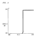
- FIG. 3 shows the current-voltage characteristic curve for an antifuse with the current plotted vertically in units of ⁇ amps versus the voltage plotted horizontally in units of volts.
- dopant material Ti
- Ti dopant material
- the antifuse was open before the curve was obtained, and the cureve was made during programming.
- the current is negligible, less than 1 ⁇ amp, until the programming voltage of about 11 volts is reached. At this value, the current rises abruptly to its closed circuit value, i.e., the ON state.
- a voltage above threshold is desirably used to compensate for any variations in anises.
- the open circuit resistance depends in well-known manner on the size of the via, it was found that the closed circuit resistance is relatively independent of the via diameter. This indicates that the programming creates relatively localized current paths through the antifuse. This may impose a limitation on the current density in the via.
- contact antifuses may be fabricated.
- the first electrically conducting section comprises an active region of a device.
- other amorphous Group IV semiconductors such as Ge and Sn, might be used.
- the dopant material might be adjacent to the first; rather than the second, electrically conducting section.
- the variation in ON state resistance, due to its polarty dependence, makes multi-level logic applications possible.
- Other resistivity increasing dopants, such as F, may also be used.
- the resistivity-increasing dopant may be omitted if the amorphous silicon has a resistivity of at least 50 x 104 ohm . cm.
Landscapes
- Design And Manufacture Of Integrated Circuits (AREA)
- Semiconductor Memories (AREA)
Applications Claiming Priority (2)
| Application Number | Priority Date | Filing Date | Title |
|---|---|---|---|
| US51590590A | 1990-04-30 | 1990-04-30 | |
| US515905 | 1990-04-30 |
Publications (1)
| Publication Number | Publication Date |
|---|---|
| EP0455414A1 true EP0455414A1 (de) | 1991-11-06 |
Family
ID=24053259
Family Applications (1)
| Application Number | Title | Priority Date | Filing Date |
|---|---|---|---|
| EP91303714A Withdrawn EP0455414A1 (de) | 1990-04-30 | 1991-04-24 | Integrierte Schaltungen mit Antischmelzsicherungen |
Country Status (3)
| Country | Link |
|---|---|
| EP (1) | EP0455414A1 (de) |
| JP (1) | JPH04229635A (de) |
| KR (1) | KR910019241A (de) |
Cited By (32)
| Publication number | Priority date | Publication date | Assignee | Title |
|---|---|---|---|---|
| EP0558176A1 (de) * | 1992-02-26 | 1993-09-01 | Actel Corporation | Metall-Metall-Antischmelzsicherung mit verbesserter Diffusionsbarriere-Schicht |
| WO1995014310A1 (en) * | 1993-11-19 | 1995-05-26 | Crosspoint Solutions, Inc. | Antifuse with doped barrier metal layer |
| US5464790A (en) * | 1992-09-23 | 1995-11-07 | Actel Corporation | Method of fabricating an antifuse element having an etch-stop dielectric layer |
| US5482884A (en) * | 1992-12-17 | 1996-01-09 | Actel Corporation | Low-temperature process metal-to-metal antifuse employing silicon link |
| US5508220A (en) * | 1991-04-18 | 1996-04-16 | Actel Corporation | Method of forming antifuses having minimum areas |
| US5519248A (en) * | 1993-07-07 | 1996-05-21 | Actel Corporation | Circuits for ESD protection of metal-to-metal antifuses during processing |
| US5525830A (en) * | 1992-09-23 | 1996-06-11 | Actel Corporation | Metal-to-metal antifuse including etch stop layer |
| US5541441A (en) * | 1994-10-06 | 1996-07-30 | Actel Corporation | Metal to metal antifuse |
| US5543656A (en) * | 1990-04-12 | 1996-08-06 | Actel Corporation | Metal to metal antifuse |
| US5552627A (en) * | 1990-04-12 | 1996-09-03 | Actel Corporation | Electrically programmable antifuse incorporating dielectric and amorphous silicon interlayers |
| EP0680087A3 (de) * | 1994-04-28 | 1996-10-02 | Canon Kk | Halbleiterbauelement, welches eine Silizidreaktion ausnutzt, um anpassbare Verbindungen herzustellen. |
| US5576576A (en) * | 1992-11-04 | 1996-11-19 | Actel Corporation | Above via metal-to-metal antifuse |
| US5592016A (en) * | 1995-04-14 | 1997-01-07 | Actel Corporation | Antifuse with improved antifuse material |
| US5614756A (en) | 1990-04-12 | 1997-03-25 | Actel Corporation | Metal-to-metal antifuse with conductive |
| US5633189A (en) * | 1994-08-01 | 1997-05-27 | Actel Corporation | Method of making metal to metal antifuse |
| US5670818A (en) * | 1990-04-12 | 1997-09-23 | Actel Corporation | Electrically programmable antifuse |
| US5741720A (en) * | 1995-10-04 | 1998-04-21 | Actel Corporation | Method of programming an improved metal-to-metal via-type antifuse |
| US5763299A (en) * | 1995-06-06 | 1998-06-09 | Actel Corporation | Reduced leakage antifuse fabrication method |
| US5780323A (en) | 1990-04-12 | 1998-07-14 | Actel Corporation | Fabrication method for metal-to-metal antifuses incorporating a tungsten via plug |
| US5789764A (en) * | 1995-04-14 | 1998-08-04 | Actel Corporation | Antifuse with improved antifuse material |
| US5793094A (en) * | 1995-12-28 | 1998-08-11 | Vlsi Technology, Inc. | Methods for fabricating anti-fuse structures |
| US5804500A (en) * | 1995-06-02 | 1998-09-08 | Actel Corporation | Fabrication process for raised tungsten plug antifuse |
| US5856234A (en) * | 1993-09-14 | 1999-01-05 | Actel Corporation | Method of fabricating an antifuse |
| US5899707A (en) * | 1996-08-20 | 1999-05-04 | Vlsi Technology, Inc. | Method for making doped antifuse structures |
| US5913137A (en) * | 1993-07-07 | 1999-06-15 | Actel Corporation | Process ESD protection devices for use with antifuses |
| US6111302A (en) | 1993-11-22 | 2000-08-29 | Actel Corporation | Antifuse structure suitable for VLSI application |
| US6150705A (en) * | 1993-07-07 | 2000-11-21 | Actel Corporation | Dielectric-polysilicon-dielectric-polysilicon-dielectric antifuse for field programmable logic application |
| US6171512B1 (en) | 1991-02-15 | 2001-01-09 | Canon Kabushiki Kaisha | Etching solution for etching porous silicon, etching method using the etching solution and method of preparing semiconductor member using the etching solution |
| US6898101B1 (en) | 1997-12-16 | 2005-05-24 | Cypress Semiconductor Corp. | Microcontroller with programmable logic on a single chip |
| US6912601B1 (en) | 2000-06-28 | 2005-06-28 | Cypress Semiconductor Corp. | Method of programming PLDs using a wireless link |
| US7884672B1 (en) | 2006-11-01 | 2011-02-08 | Cypress Semiconductor Corporation | Operational amplifier and method for amplifying a signal with shared compensation components |
| CN105022546A (zh) * | 2009-06-11 | 2015-11-04 | 株式会社村田制作所 | 触摸面板以及触摸式输入装置 |
Families Citing this family (4)
| Publication number | Priority date | Publication date | Assignee | Title |
|---|---|---|---|---|
| US5314840A (en) * | 1992-12-18 | 1994-05-24 | International Business Machines Corporation | Method for forming an antifuse element with electrical or optical programming |
| KR100328709B1 (ko) * | 1999-07-07 | 2002-03-20 | 박종섭 | 프로그래밍 부위 형성방법 |
| JP4489363B2 (ja) * | 2003-03-03 | 2010-06-23 | シャープ株式会社 | 不揮発性記憶素子、不揮発性記憶回路、不揮発性記憶カードおよび記録再生装置 |
| WO2018025691A1 (ja) * | 2016-08-04 | 2018-02-08 | 日本電気株式会社 | 整流素子及び該整流素子を有するスイッチング素子 |
Citations (6)
| Publication number | Priority date | Publication date | Assignee | Title |
|---|---|---|---|---|
| EP0036802A1 (de) * | 1980-03-24 | 1981-09-30 | COMMISSARIAT A L'ENERGIE ATOMIQUE Etablissement de Caractère Scientifique Technique et Industriel | Verfahren zur Herstellung amorpher Halbleiter-Speicheranordnungen |
| GB2086654A (en) * | 1980-10-28 | 1982-05-12 | Energy Conversion Devices Inc | Programmable cells and arrays |
| US4569121A (en) * | 1983-03-07 | 1986-02-11 | Signetics Corporation | Method of fabricating a programmable read-only memory cell incorporating an antifuse utilizing deposition of amorphous semiconductor layer |
| WO1987002827A1 (en) * | 1985-10-29 | 1987-05-07 | 4C Electronics, Inc. | Programmable integrated crosspoint switch |
| EP0323078A2 (de) * | 1987-12-28 | 1989-07-05 | Actel Corporation | Elektrisch programmierbare Antischmelzsicherung niedriger Impedanz |
| EP0414361A2 (de) * | 1989-08-24 | 1991-02-27 | Advanced Micro Devices, Inc. | Halbleitende Antischmelzsicherungsstruktur und Verfahren |
-
1991
- 1991-04-23 KR KR1019910006476A patent/KR910019241A/ko not_active Withdrawn
- 1991-04-24 EP EP91303714A patent/EP0455414A1/de not_active Withdrawn
- 1991-04-30 JP JP3097835A patent/JPH04229635A/ja not_active Withdrawn
Patent Citations (6)
| Publication number | Priority date | Publication date | Assignee | Title |
|---|---|---|---|---|
| EP0036802A1 (de) * | 1980-03-24 | 1981-09-30 | COMMISSARIAT A L'ENERGIE ATOMIQUE Etablissement de Caractère Scientifique Technique et Industriel | Verfahren zur Herstellung amorpher Halbleiter-Speicheranordnungen |
| GB2086654A (en) * | 1980-10-28 | 1982-05-12 | Energy Conversion Devices Inc | Programmable cells and arrays |
| US4569121A (en) * | 1983-03-07 | 1986-02-11 | Signetics Corporation | Method of fabricating a programmable read-only memory cell incorporating an antifuse utilizing deposition of amorphous semiconductor layer |
| WO1987002827A1 (en) * | 1985-10-29 | 1987-05-07 | 4C Electronics, Inc. | Programmable integrated crosspoint switch |
| EP0323078A2 (de) * | 1987-12-28 | 1989-07-05 | Actel Corporation | Elektrisch programmierbare Antischmelzsicherung niedriger Impedanz |
| EP0414361A2 (de) * | 1989-08-24 | 1991-02-27 | Advanced Micro Devices, Inc. | Halbleitende Antischmelzsicherungsstruktur und Verfahren |
Cited By (45)
| Publication number | Priority date | Publication date | Assignee | Title |
|---|---|---|---|---|
| US5770885A (en) * | 1990-04-12 | 1998-06-23 | Actel Corporation | Electrically programmable antifuse incorporating dielectric and amorphous silicon interlayers |
| US5543656A (en) * | 1990-04-12 | 1996-08-06 | Actel Corporation | Metal to metal antifuse |
| US5780323A (en) | 1990-04-12 | 1998-07-14 | Actel Corporation | Fabrication method for metal-to-metal antifuses incorporating a tungsten via plug |
| US5763898A (en) | 1990-04-12 | 1998-06-09 | Actel Corporation | Above via metal-to-metal antifuses incorporating a tungsten via plug |
| US5552627A (en) * | 1990-04-12 | 1996-09-03 | Actel Corporation | Electrically programmable antifuse incorporating dielectric and amorphous silicon interlayers |
| US5670818A (en) * | 1990-04-12 | 1997-09-23 | Actel Corporation | Electrically programmable antifuse |
| US5614756A (en) | 1990-04-12 | 1997-03-25 | Actel Corporation | Metal-to-metal antifuse with conductive |
| US6171512B1 (en) | 1991-02-15 | 2001-01-09 | Canon Kabushiki Kaisha | Etching solution for etching porous silicon, etching method using the etching solution and method of preparing semiconductor member using the etching solution |
| US5508220A (en) * | 1991-04-18 | 1996-04-16 | Actel Corporation | Method of forming antifuses having minimum areas |
| US5510646A (en) * | 1992-02-26 | 1996-04-23 | Actel Corporation | Metal-to-metal antifuse with improved diffusion barrier layer |
| EP0558176A1 (de) * | 1992-02-26 | 1993-09-01 | Actel Corporation | Metall-Metall-Antischmelzsicherung mit verbesserter Diffusionsbarriere-Schicht |
| US5753528A (en) * | 1992-02-26 | 1998-05-19 | Actel Corporation | Method of fabricating metal-to-metal antifuse with improved diffusion barrier layer |
| US5525830A (en) * | 1992-09-23 | 1996-06-11 | Actel Corporation | Metal-to-metal antifuse including etch stop layer |
| US5464790A (en) * | 1992-09-23 | 1995-11-07 | Actel Corporation | Method of fabricating an antifuse element having an etch-stop dielectric layer |
| US5576576A (en) * | 1992-11-04 | 1996-11-19 | Actel Corporation | Above via metal-to-metal antifuse |
| US5482884A (en) * | 1992-12-17 | 1996-01-09 | Actel Corporation | Low-temperature process metal-to-metal antifuse employing silicon link |
| US5519248A (en) * | 1993-07-07 | 1996-05-21 | Actel Corporation | Circuits for ESD protection of metal-to-metal antifuses during processing |
| US5913137A (en) * | 1993-07-07 | 1999-06-15 | Actel Corporation | Process ESD protection devices for use with antifuses |
| US5825072A (en) * | 1993-07-07 | 1998-10-20 | Actel Corporation | Circuits for ESD Protection of metal to-metal antifuses during processing |
| US6150705A (en) * | 1993-07-07 | 2000-11-21 | Actel Corporation | Dielectric-polysilicon-dielectric-polysilicon-dielectric antifuse for field programmable logic application |
| US5856234A (en) * | 1993-09-14 | 1999-01-05 | Actel Corporation | Method of fabricating an antifuse |
| WO1995014310A1 (en) * | 1993-11-19 | 1995-05-26 | Crosspoint Solutions, Inc. | Antifuse with doped barrier metal layer |
| US5523612A (en) * | 1993-11-19 | 1996-06-04 | Crosspoint Solutions, Inc. | Method of manufacturing an antifuse with doped barrier metal layer and resulting antifuse |
| US6111302A (en) | 1993-11-22 | 2000-08-29 | Actel Corporation | Antifuse structure suitable for VLSI application |
| EP0680087A3 (de) * | 1994-04-28 | 1996-10-02 | Canon Kk | Halbleiterbauelement, welches eine Silizidreaktion ausnutzt, um anpassbare Verbindungen herzustellen. |
| US6051851A (en) * | 1994-04-28 | 2000-04-18 | Canon Kabushiki Kaisha | Semiconductor devices utilizing silicide reaction |
| US5633189A (en) * | 1994-08-01 | 1997-05-27 | Actel Corporation | Method of making metal to metal antifuse |
| US6001693A (en) * | 1994-10-06 | 1999-12-14 | Yeouchung; Yen | Method of making a metal to metal antifuse |
| US5541441A (en) * | 1994-10-06 | 1996-07-30 | Actel Corporation | Metal to metal antifuse |
| US5592016A (en) * | 1995-04-14 | 1997-01-07 | Actel Corporation | Antifuse with improved antifuse material |
| US5789764A (en) * | 1995-04-14 | 1998-08-04 | Actel Corporation | Antifuse with improved antifuse material |
| US6124193A (en) | 1995-06-02 | 2000-09-26 | Actel Corporation | Raised tungsten plug antifuse and fabrication processes |
| US5920109A (en) | 1995-06-02 | 1999-07-06 | Actel Corporation | Raised tungsten plug antifuse and fabrication processes |
| US5804500A (en) * | 1995-06-02 | 1998-09-08 | Actel Corporation | Fabrication process for raised tungsten plug antifuse |
| US5986322A (en) * | 1995-06-06 | 1999-11-16 | Mccollum; John L. | Reduced leakage antifuse structure |
| US5763299A (en) * | 1995-06-06 | 1998-06-09 | Actel Corporation | Reduced leakage antifuse fabrication method |
| US5741720A (en) * | 1995-10-04 | 1998-04-21 | Actel Corporation | Method of programming an improved metal-to-metal via-type antifuse |
| US5962910A (en) | 1995-10-04 | 1999-10-05 | Actel Corporation | Metal-to-metal via-type antifuse |
| US5793094A (en) * | 1995-12-28 | 1998-08-11 | Vlsi Technology, Inc. | Methods for fabricating anti-fuse structures |
| US5899707A (en) * | 1996-08-20 | 1999-05-04 | Vlsi Technology, Inc. | Method for making doped antifuse structures |
| US6898101B1 (en) | 1997-12-16 | 2005-05-24 | Cypress Semiconductor Corp. | Microcontroller with programmable logic on a single chip |
| US7480165B1 (en) | 1997-12-16 | 2009-01-20 | Mann Eric N | Microcontroller with programmable logic |
| US6912601B1 (en) | 2000-06-28 | 2005-06-28 | Cypress Semiconductor Corp. | Method of programming PLDs using a wireless link |
| US7884672B1 (en) | 2006-11-01 | 2011-02-08 | Cypress Semiconductor Corporation | Operational amplifier and method for amplifying a signal with shared compensation components |
| CN105022546A (zh) * | 2009-06-11 | 2015-11-04 | 株式会社村田制作所 | 触摸面板以及触摸式输入装置 |
Also Published As
| Publication number | Publication date |
|---|---|
| KR910019241A (ko) | 1991-11-30 |
| JPH04229635A (ja) | 1992-08-19 |
Similar Documents
| Publication | Publication Date | Title |
|---|---|---|
| EP0455414A1 (de) | Integrierte Schaltungen mit Antischmelzsicherungen | |
| KR0162073B1 (ko) | 프로그램 가능한 저 임피던스 상호 접속 회로 소자 | |
| JP3095811B2 (ja) | 電気的プログラム可能な非融解型素子、該素子を含む半導体デバイス、及び該素子の形成方法 | |
| US4943538A (en) | Programmable low impedance anti-fuse element | |
| US5163180A (en) | Low voltage programming antifuse and transistor breakdown method for making same | |
| US5100827A (en) | Buried antifuse | |
| US5485031A (en) | Antifuse structure suitable for VLSI application | |
| US5411917A (en) | Electrically programmable antifuse incorporating dielectric and amorphous silicon interlayer | |
| JP3204454B2 (ja) | 電界効果トランジスタの選択的プログラミング方法 | |
| US5095362A (en) | Method for reducing resistance for programmed antifuse | |
| US6525399B2 (en) | Junctionless antifuses and systems containing junctionless antifuses | |
| JP3256603B2 (ja) | 半導体装置及びその製造方法 | |
| US5670403A (en) | Dielectric-polysilicon-dielectric antifuse for field programmable logic applications | |
| US4499557A (en) | Programmable cell for use in programmable electronic arrays | |
| US5391518A (en) | Method of making a field programmable read only memory (ROM) cell using an amorphous silicon fuse with buried contact polysilicon and metal electrodes | |
| US20070029576A1 (en) | Programmable semiconductor device containing a vertically notched fusible link region and methods of making and using same | |
| US5210598A (en) | Semiconductor element having a resistance state transition region of two-layer structure | |
| US5821558A (en) | Antifuse structures | |
| KR20070106962A (ko) | 다이오드를 구비하는 퓨즈 메모리 셀과, 퓨즈 소자로작용하는 다이오드 | |
| JPH06510634A (ja) | アモルファスシリコンアンチヒューズ及びその製造方法 | |
| JPH0756884B2 (ja) | 半導体素子の製造方法 | |
| JPS6249651A (ja) | アンチヒユ−ズ、その製法、電気的にプログラム可能なメモリ・セル、メモリ・セルをプログラムする方法 | |
| JPH0574947A (ja) | 半導体装置 |
Legal Events
| Date | Code | Title | Description |
|---|---|---|---|
| PUAI | Public reference made under article 153(3) epc to a published international application that has entered the european phase |
Free format text: ORIGINAL CODE: 0009012 |
|
| AK | Designated contracting states |
Kind code of ref document: A1 Designated state(s): DE ES FR GB |
|
| 17P | Request for examination filed |
Effective date: 19920427 |
|
| 17Q | First examination report despatched |
Effective date: 19940406 |
|
| RAP3 | Party data changed (applicant data changed or rights of an application transferred) |
Owner name: AT&T CORP. |
|
| STAA | Information on the status of an ep patent application or granted ep patent |
Free format text: STATUS: THE APPLICATION IS DEEMED TO BE WITHDRAWN |
|
| 18D | Application deemed to be withdrawn |
Effective date: 19950905 |