EP0036802A1 - Verfahren zur Herstellung amorpher Halbleiter-Speicheranordnungen - Google Patents
Verfahren zur Herstellung amorpher Halbleiter-Speicheranordnungen Download PDFInfo
- Publication number
- EP0036802A1 EP0036802A1 EP81400378A EP81400378A EP0036802A1 EP 0036802 A1 EP0036802 A1 EP 0036802A1 EP 81400378 A EP81400378 A EP 81400378A EP 81400378 A EP81400378 A EP 81400378A EP 0036802 A1 EP0036802 A1 EP 0036802A1
- Authority
- EP
- European Patent Office
- Prior art keywords
- layer
- compound
- amorphous semiconductor
- constituting
- proper
- Prior art date
- Legal status (The legal status is an assumption and is not a legal conclusion. Google has not performed a legal analysis and makes no representation as to the accuracy of the status listed.)
- Granted
Links
- 239000004065 semiconductor Substances 0.000 title claims abstract description 33
- 238000004519 manufacturing process Methods 0.000 title claims abstract description 11
- 150000001875 compounds Chemical class 0.000 claims abstract description 36
- 230000004888 barrier function Effects 0.000 claims abstract description 22
- 230000003446 memory effect Effects 0.000 claims abstract description 11
- 239000000758 substrate Substances 0.000 claims abstract description 8
- 229910052751 metal Inorganic materials 0.000 claims abstract description 7
- 239000002184 metal Substances 0.000 claims abstract description 7
- 238000000034 method Methods 0.000 claims description 15
- GUVRBAGPIYLISA-UHFFFAOYSA-N tantalum atom Chemical compound [Ta] GUVRBAGPIYLISA-UHFFFAOYSA-N 0.000 claims description 9
- 229910052715 tantalum Inorganic materials 0.000 claims description 8
- WFKWXMTUELFFGS-UHFFFAOYSA-N tungsten Chemical compound [W] WFKWXMTUELFFGS-UHFFFAOYSA-N 0.000 claims description 8
- 229910052721 tungsten Inorganic materials 0.000 claims description 8
- 239000010937 tungsten Substances 0.000 claims description 8
- 239000000203 mixture Substances 0.000 claims description 7
- PORWMNRCUJJQNO-UHFFFAOYSA-N tellurium atom Chemical compound [Te] PORWMNRCUJJQNO-UHFFFAOYSA-N 0.000 claims description 7
- 229910052714 tellurium Inorganic materials 0.000 claims description 6
- 229910052581 Si3N4 Inorganic materials 0.000 claims description 5
- NINIDFKCEFEMDL-UHFFFAOYSA-N Sulfur Chemical compound [S] NINIDFKCEFEMDL-UHFFFAOYSA-N 0.000 claims description 5
- 239000011521 glass Substances 0.000 claims description 5
- HQVNEWCFYHHQES-UHFFFAOYSA-N silicon nitride Chemical compound N12[Si]34N5[Si]62N3[Si]51N64 HQVNEWCFYHHQES-UHFFFAOYSA-N 0.000 claims description 5
- HPQRSQFZILKRDH-UHFFFAOYSA-M chloro(trimethyl)plumbane Chemical compound C[Pb](C)(C)Cl HPQRSQFZILKRDH-UHFFFAOYSA-M 0.000 claims description 4
- 230000006641 stabilisation Effects 0.000 claims description 4
- 229910052717 sulfur Inorganic materials 0.000 claims description 4
- 239000011593 sulfur Substances 0.000 claims description 4
- HQZPMWBCDLCGCL-UHFFFAOYSA-N tantalum telluride Chemical compound [Te]=[Ta]=[Te] HQZPMWBCDLCGCL-UHFFFAOYSA-N 0.000 claims description 4
- 229910052782 aluminium Inorganic materials 0.000 claims description 3
- XAGFODPZIPBFFR-UHFFFAOYSA-N aluminium Chemical compound [Al] XAGFODPZIPBFFR-UHFFFAOYSA-N 0.000 claims description 3
- 229910052785 arsenic Inorganic materials 0.000 claims description 3
- 229910052732 germanium Inorganic materials 0.000 claims description 3
- GNPVGFCGXDBREM-UHFFFAOYSA-N germanium atom Chemical compound [Ge] GNPVGFCGXDBREM-UHFFFAOYSA-N 0.000 claims description 3
- 238000011105 stabilization Methods 0.000 claims description 3
- RQNWIZPPADIBDY-UHFFFAOYSA-N arsenic atom Chemical compound [As] RQNWIZPPADIBDY-UHFFFAOYSA-N 0.000 claims description 2
- 239000000463 material Substances 0.000 abstract description 7
- 238000003860 storage Methods 0.000 abstract description 3
- 238000009792 diffusion process Methods 0.000 description 6
- 238000000151 deposition Methods 0.000 description 4
- 230000000694 effects Effects 0.000 description 4
- 239000011148 porous material Substances 0.000 description 3
- XKRFYHLGVUSROY-UHFFFAOYSA-N Argon Chemical compound [Ar] XKRFYHLGVUSROY-UHFFFAOYSA-N 0.000 description 2
- 230000008021 deposition Effects 0.000 description 2
- 238000005530 etching Methods 0.000 description 2
- 208000031968 Cadaver Diseases 0.000 description 1
- OKTJSMMVPCPJKN-UHFFFAOYSA-N Carbon Chemical compound [C] OKTJSMMVPCPJKN-UHFFFAOYSA-N 0.000 description 1
- ZOKXTWBITQBERF-UHFFFAOYSA-N Molybdenum Chemical compound [Mo] ZOKXTWBITQBERF-UHFFFAOYSA-N 0.000 description 1
- 229910052786 argon Inorganic materials 0.000 description 1
- QVGXLLKOCUKJST-UHFFFAOYSA-N atomic oxygen Chemical compound [O] QVGXLLKOCUKJST-UHFFFAOYSA-N 0.000 description 1
- 230000015572 biosynthetic process Effects 0.000 description 1
- 229910052799 carbon Inorganic materials 0.000 description 1
- 239000004020 conductor Substances 0.000 description 1
- 230000007547 defect Effects 0.000 description 1
- 238000005137 deposition process Methods 0.000 description 1
- 238000001035 drying Methods 0.000 description 1
- 230000003628 erosive effect Effects 0.000 description 1
- 239000011810 insulating material Substances 0.000 description 1
- 229910052750 molybdenum Inorganic materials 0.000 description 1
- 239000011733 molybdenum Substances 0.000 description 1
- 229910052760 oxygen Inorganic materials 0.000 description 1
- 239000001301 oxygen Substances 0.000 description 1
- FAWYJKSBSAKOFP-UHFFFAOYSA-N tantalum(iv) sulfide Chemical class S=[Ta]=S FAWYJKSBSAKOFP-UHFFFAOYSA-N 0.000 description 1
- ITRNXVSDJBHYNJ-UHFFFAOYSA-N tungsten disulfide Chemical compound S=[W]=S ITRNXVSDJBHYNJ-UHFFFAOYSA-N 0.000 description 1
Images
Classifications
-
- H—ELECTRICITY
- H10—SEMICONDUCTOR DEVICES; ELECTRIC SOLID-STATE DEVICES NOT OTHERWISE PROVIDED FOR
- H10N—ELECTRIC SOLID-STATE DEVICES NOT OTHERWISE PROVIDED FOR
- H10N70/00—Solid-state devices having no potential barriers, and specially adapted for rectifying, amplifying, oscillating or switching
- H10N70/20—Multistable switching devices, e.g. memristors
-
- H—ELECTRICITY
- H10—SEMICONDUCTOR DEVICES; ELECTRIC SOLID-STATE DEVICES NOT OTHERWISE PROVIDED FOR
- H10N—ELECTRIC SOLID-STATE DEVICES NOT OTHERWISE PROVIDED FOR
- H10N70/00—Solid-state devices having no potential barriers, and specially adapted for rectifying, amplifying, oscillating or switching
- H10N70/801—Constructional details of multistable switching devices
-
- H—ELECTRICITY
- H10—SEMICONDUCTOR DEVICES; ELECTRIC SOLID-STATE DEVICES NOT OTHERWISE PROVIDED FOR
- H10N—ELECTRIC SOLID-STATE DEVICES NOT OTHERWISE PROVIDED FOR
- H10N70/00—Solid-state devices having no potential barriers, and specially adapted for rectifying, amplifying, oscillating or switching
- H10N70/801—Constructional details of multistable switching devices
- H10N70/821—Device geometry
- H10N70/826—Device geometry adapted for essentially vertical current flow, e.g. sandwich or pillar type devices
-
- H—ELECTRICITY
- H10—SEMICONDUCTOR DEVICES; ELECTRIC SOLID-STATE DEVICES NOT OTHERWISE PROVIDED FOR
- H10N—ELECTRIC SOLID-STATE DEVICES NOT OTHERWISE PROVIDED FOR
- H10N70/00—Solid-state devices having no potential barriers, and specially adapted for rectifying, amplifying, oscillating or switching
- H10N70/801—Constructional details of multistable switching devices
- H10N70/841—Electrodes
-
- H—ELECTRICITY
- H10—SEMICONDUCTOR DEVICES; ELECTRIC SOLID-STATE DEVICES NOT OTHERWISE PROVIDED FOR
- H10N—ELECTRIC SOLID-STATE DEVICES NOT OTHERWISE PROVIDED FOR
- H10N70/00—Solid-state devices having no potential barriers, and specially adapted for rectifying, amplifying, oscillating or switching
- H10N70/801—Constructional details of multistable switching devices
- H10N70/881—Switching materials
- H10N70/882—Compounds of sulfur, selenium or tellurium, e.g. chalcogenides
-
- Y—GENERAL TAGGING OF NEW TECHNOLOGICAL DEVELOPMENTS; GENERAL TAGGING OF CROSS-SECTIONAL TECHNOLOGIES SPANNING OVER SEVERAL SECTIONS OF THE IPC; TECHNICAL SUBJECTS COVERED BY FORMER USPC CROSS-REFERENCE ART COLLECTIONS [XRACs] AND DIGESTS
- Y10—TECHNICAL SUBJECTS COVERED BY FORMER USPC
- Y10S—TECHNICAL SUBJECTS COVERED BY FORMER USPC CROSS-REFERENCE ART COLLECTIONS [XRACs] AND DIGESTS
- Y10S148/00—Metal treatment
- Y10S148/084—Ion implantation of compound devices
-
- Y—GENERAL TAGGING OF NEW TECHNOLOGICAL DEVELOPMENTS; GENERAL TAGGING OF CROSS-SECTIONAL TECHNOLOGIES SPANNING OVER SEVERAL SECTIONS OF THE IPC; TECHNICAL SUBJECTS COVERED BY FORMER USPC CROSS-REFERENCE ART COLLECTIONS [XRACs] AND DIGESTS
- Y10—TECHNICAL SUBJECTS COVERED BY FORMER USPC
- Y10S—TECHNICAL SUBJECTS COVERED BY FORMER USPC CROSS-REFERENCE ART COLLECTIONS [XRACs] AND DIGESTS
- Y10S438/00—Semiconductor device manufacturing: process
- Y10S438/90—Bulk effect device making
-
- Y—GENERAL TAGGING OF NEW TECHNOLOGICAL DEVELOPMENTS; GENERAL TAGGING OF CROSS-SECTIONAL TECHNOLOGIES SPANNING OVER SEVERAL SECTIONS OF THE IPC; TECHNICAL SUBJECTS COVERED BY FORMER USPC CROSS-REFERENCE ART COLLECTIONS [XRACs] AND DIGESTS
- Y10—TECHNICAL SUBJECTS COVERED BY FORMER USPC
- Y10S—TECHNICAL SUBJECTS COVERED BY FORMER USPC CROSS-REFERENCE ART COLLECTIONS [XRACs] AND DIGESTS
- Y10S438/00—Semiconductor device manufacturing: process
- Y10S438/93—Ternary or quaternary semiconductor comprised of elements from three different groups, e.g. I-III-V
Definitions
- the present invention relates to a method for producing memory effect devices with amorphous semiconductors.
- the present invention relates to the production of amorphous semiconductor components used for electrical storage.
- amorphous semiconductor devices comprise a substrate on which is deposited a lower electrode, an active area produced using an amorphous semiconductor compound and an upper electrode.
- amorphous semiconductor devices for example, of the "pore” type or of the "three layers” type, as well as the various methods making it possible, have been described in French Patent No. 2,365,888 filed on September 28 1976 on behalf of the French Atomic Energy Commission and entitled “Process for producing amorphous semiconductor devices and devices using them", as well as in the certificate of addition of this same patent No. 2,389,239 filed April 27, 1977.
- these different types of semiconductor devices can have a storage effect or a switching effect depending on their structure.
- Electrodes made of Carbon are currently used, but these electrodes have various drawbacks and in particular a poor ability for this memory effect.
- this material is difficult to deposit, if one wishes a layer without constraint, without defect and not evolving over time with the electrical or thermal pulses which are imposed on it, when using such a device.
- this material very easily traps the oxygen present on the substrate and the different layers of the other materials constituting the semiconductor, which imposes certain conditions in the deposition process, during the production of the semiconductor.
- the present invention aims to remedy these drawbacks and in particular to allow the production of semiconductor devices whose electrodes have a good ability to the memory effect and whose deposition of these electrodes is easily achievable.
- At least one of the barrier layers is made of tantalum telluride or of tungsten telluride.
- the first amorphous compound, constituting the active layer proper is produced by glass of composition Te79 Gel7 S 2 Sb 2 .
- the second amorphous semiconductor compound constituting the buffer layers is produced by glass of composition Te60 As 25 Ge 13 S 1 .
- an insulating layer is deposited over one or the other of the electrodes proper.
- This insulating layer is preferably made of Silicon Nitride.
- the upper electrode proper can be covered with a conductive layer of aluminum.
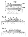
- the reference 2 represents the substrate on which the semiconductor device is produced
- the reference 4 represents the lower electrode
- the reference 6 represents the active area produced using an amorphous semiconductor compound
- the reference 8 an upper electrode.
- the electrodes 4 and 8 and the active area 6 have a more complex structure.
- the lower electrode 4 comprises an actual electrode 4a, directly in contact with the substrate 2 and a thin layer 4b facing the active area 6 and constituting a barrier.
- the upper electrode 8 comprises an actual electrode 8a, and a thin layer 8b constituting a barrier, facing the active area 6 like the barrier 4b.
- the electrodes proper 4a and 8a are made of a metal capable of forming a binary compound with a hexagonal structure, such as Tungsten or Tantalum. Indeed, these materials have the advantage of being materials capable of the memory effect.
- the barriers 4b or 8b are formed by said binary compound with a hexagonal structure. In the case of tantalum electrodes, the barriers 4b or 8b are made for example of tantalum telluride and in the case of tungsten electrodes, the barriers 4b or 8b are made for example of tungsten telluride. These barriers 4b and 8b are necessary for the stabilization of the semiconductor.
- the active zone 6 consists of an actual active layer 6a, an upper buffer layer 6b and a lower buffer layer 6c. These buffer layers 6b and 6c make it possible to avoid any diffusion of the electrode in the active area 6a.
- This active layer proper 6a is made of a compound rich in tellurium and, preferably, with glass of composition Te 79 Ge17 S 2 Sb 2 .
- the buffer layers 6b and 6c are made of a glassy compound preferably rich in tellurium and having the composition Te 60 As 21 Ge 13 S 1 .
- tellurium in the buffer layers 6b and 6c allows the formation, by diffusion, of the electrodes 4a and 8a in these buffer layers, the barrier layers 4b and 8b into a binary compound with hexagonal structure in the form of a tantalum telluride. or of a Tungsten Telluride, for electrodes 4a and 8a produced either in Tantalum or in Tungsten.
- buffer layers 6b and 6c made of a vitreous compound rich in sulfur
- barrier layers 4b and 8b in a binary compound with hexagonal structure in the form of a Tantalum Sulfide or of a Tungsten Sulfide for electrodes 4a and 8a produced either in Tantalum or in Tungsten.
- the electrodes of the same device can be of different nature, as well as the type of characteristics which it is desired to obtain for the semiconductor device amorphous, one or two barrier layers and / or one or two buffer layers can be deposited.
- the barrier layer can also be produced by diffusion, before any use of the semiconductor device. Otherwise, from the start of use of this device, the presence of a buffer layer allows the realization of this barrier layer, by diffusion of the metal electrode capable of diffusing into this buffer layer.
- the reference 10 corresponds to an insulating layer preferably made of silicon nitride and which can be placed either on a part of the upper electrode 8, said layer being referenced 10a, or on a part of the electrode. lower 4, said layer then being referenced lOb.
- the position of this insulating layer-10 depends on the type of device that is produced.
- the device according to the invention corresponds to a device of the "three layers" type.
- This device is obtained by depositing the three layers corresponding to the two electrodes 4 and 8 and to the active area 6, as described above on the substrate 2 according to known techniques.
- the deposit being made, the three layers 4, 6 and 8 are etched to the shape of the lower electrode 4, for example by mechanical erosion and by dry process, then by the same process, the upper electrode 8 so as to give it its final dimension.
- a uniform deposit of an insulating material constituting the insulating layer 10 is carried out by any known means.
- This insulating layer 10 can be made up of any compound other than an oxide.
- this insulating layer 10 is made of silicon nitride.
- the next step consists in etching the insulating layer 10, for example by bombardment of Argon.
- a window 12 above the upper electrode 8 is also defined in this insulating layer 10.
- a uniform deposit of conductive material 14 is carried out, then this deposit is etched to separate the conduction of the lower electrode 4 and the upper electrode 8.
- the active area A is thus defined by the surface of the upper electrode 8.
- the device according to the invention shown in Figure 3 corresponds to a device of the "pore" type.
- This device is obtained by depositing the lower electrode 4 on the substrate 2, then by etching this deposit to give it the desired shape. Is then carried out a uniform deposition of the insulating layer 10 preferably made of silicon nitride. Then, as above, the layer 10 is etched to provide the window 12 which defines the active area B of the semiconductor component. Next, the active layer 6 is deposited, then the conductive layer 14. Finally, the conductive layer 14 and the active layer 6 are etched to release the electrical connection plates.
- the conductive layer 14 is made, for example, of Aluminum.
- the composition of the barrier layer in the form of a binary compound with a hexagonal structure may be different, for example, for a buffer layer rich in tellurium, a compound of the type IlTe2 for a Tungsten electrode and a compound of type TaTe 2 for a tantalum electrode; for a sulfur-rich buffer layer and a tantalum electrode, a compound of the TaS 2 type is obtained and a compound of the WS 2 type for a Tungsten electrode.
- the advantage of such compounds is that they are very good diffusion retarders by virtue of their structure.
Landscapes
- Semiconductor Memories (AREA)
- Bipolar Transistors (AREA)
Applications Claiming Priority (2)
| Application Number | Priority Date | Filing Date | Title |
|---|---|---|---|
| FR8006480 | 1980-03-24 | ||
| FR8006480A FR2478879A1 (fr) | 1980-03-24 | 1980-03-24 | Procede de realisation de dispositifs a effet memoire a semi-conducteurs amorphes |
Publications (2)
| Publication Number | Publication Date |
|---|---|
| EP0036802A1 true EP0036802A1 (de) | 1981-09-30 |
| EP0036802B1 EP0036802B1 (de) | 1984-08-08 |
Family
ID=9240006
Family Applications (1)
| Application Number | Title | Priority Date | Filing Date |
|---|---|---|---|
| EP81400378A Expired EP0036802B1 (de) | 1980-03-24 | 1981-03-11 | Verfahren zur Herstellung amorpher Halbleiter-Speicheranordnungen |
Country Status (5)
| Country | Link |
|---|---|
| US (1) | US4366614A (de) |
| EP (1) | EP0036802B1 (de) |
| JP (1) | JPS56147493A (de) |
| DE (1) | DE3165324D1 (de) |
| FR (1) | FR2478879A1 (de) |
Cited By (4)
| Publication number | Priority date | Publication date | Assignee | Title |
|---|---|---|---|---|
| EP0455414A1 (de) * | 1990-04-30 | 1991-11-06 | AT&T Corp. | Integrierte Schaltungen mit Antischmelzsicherungen |
| EP2057683A4 (de) * | 2006-08-08 | 2010-03-10 | Nantero Inc | Speicherelemente und schnittpunktschalter sowie arrays davon mit nicht flüchtigen nanoröhrchenblöcken |
| US7835170B2 (en) | 2005-05-09 | 2010-11-16 | Nantero, Inc. | Memory elements and cross point switches and arrays of same using nonvolatile nanotube blocks |
| US9666272B2 (en) | 2009-08-06 | 2017-05-30 | Nantero Inc. | Resistive change element arrays using resistive reference elements |
Families Citing this family (16)
| Publication number | Priority date | Publication date | Assignee | Title |
|---|---|---|---|---|
| US4433342A (en) * | 1981-04-06 | 1984-02-21 | Harris Corporation | Amorphous switching device with residual crystallization retardation |
| FR2533072B1 (fr) * | 1982-09-14 | 1986-07-18 | Coissard Pierre | Procede de fabrication de circuits electroniques a base de transistors en couches minces et de condensateurs |
| US4545111A (en) * | 1983-01-18 | 1985-10-08 | Energy Conversion Devices, Inc. | Method for making, parallel preprogramming or field programming of electronic matrix arrays |
| US4677742A (en) * | 1983-01-18 | 1987-07-07 | Energy Conversion Devices, Inc. | Electronic matrix arrays and method for making the same |
| US4847732A (en) * | 1983-09-15 | 1989-07-11 | Mosaic Systems, Inc. | Wafer and method of making same |
| EP0464866A3 (en) * | 1984-02-21 | 1992-07-15 | Mosaic Systems, Inc. | Wafer and method of making same |
| US4845533A (en) * | 1986-08-22 | 1989-07-04 | Energy Conversion Devices, Inc. | Thin film electrical devices with amorphous carbon electrodes and method of making same |
| AUPO613797A0 (en) * | 1997-04-09 | 1997-05-08 | University Of Sydney, The | Digital information storage |
| DE10023116B4 (de) * | 2000-05-11 | 2005-12-15 | Infineon Technologies Ag | Feldeffekttransistor-Struktur mit isoliertem Gate |
| US7381611B2 (en) * | 2003-08-04 | 2008-06-03 | Intel Corporation | Multilayered phase change memory |
| US7482616B2 (en) * | 2004-05-27 | 2009-01-27 | Samsung Electronics Co., Ltd. | Semiconductor devices having phase change memory cells, electronic systems employing the same and methods of fabricating the same |
| DE102005025209B4 (de) * | 2004-05-27 | 2011-01-13 | Samsung Electronics Co., Ltd., Suwon | Halbleiterspeicherbauelement, elektronisches System und Verfahren zur Herstellung eines Halbleiterspeicherbauelements |
| US20050263801A1 (en) * | 2004-05-27 | 2005-12-01 | Jae-Hyun Park | Phase-change memory device having a barrier layer and manufacturing method |
| US7411208B2 (en) * | 2004-05-27 | 2008-08-12 | Samsung Electronics Co., Ltd. | Phase-change memory device having a barrier layer and manufacturing method |
| WO2009115995A1 (en) * | 2008-03-21 | 2009-09-24 | Nxp B.V. | An electronic component comprising a convertible structure |
| US8377741B2 (en) * | 2008-12-30 | 2013-02-19 | Stmicroelectronics S.R.L. | Self-heating phase change memory cell architecture |
Citations (1)
| Publication number | Priority date | Publication date | Assignee | Title |
|---|---|---|---|---|
| FR2407572A1 (fr) * | 1977-10-31 | 1979-05-25 | Burroughs Corp | Composant de memoire, amorphe, pour memoire morte |
Family Cites Families (6)
| Publication number | Priority date | Publication date | Assignee | Title |
|---|---|---|---|---|
| US3675090A (en) * | 1968-11-04 | 1972-07-04 | Energy Conversion Devices Inc | Film deposited semiconductor devices |
| US3611063A (en) * | 1969-05-16 | 1971-10-05 | Energy Conversion Devices Inc | Amorphous electrode or electrode surface |
| US3619732A (en) * | 1969-05-16 | 1971-11-09 | Energy Conversion Devices Inc | Coplanar semiconductor switch structure |
| US3886577A (en) * | 1973-09-12 | 1975-05-27 | Energy Conversion Devices Inc | Filament-type memory semiconductor device and method of making the same |
| FR2389239A2 (fr) * | 1977-04-27 | 1978-11-24 | Commissariat Energie Atomique | Procede de realisation de dispositifs semiconducteurs amorphes et dispositifs en faisant application |
| US4167806A (en) * | 1976-09-28 | 1979-09-18 | Commissariat A L'energie Atomique | Method of fabrication of an amorphous semiconductor device on a substrate |
-
1980
- 1980-03-24 FR FR8006480A patent/FR2478879A1/fr active Granted
-
1981
- 1981-03-11 EP EP81400378A patent/EP0036802B1/de not_active Expired
- 1981-03-11 DE DE8181400378T patent/DE3165324D1/de not_active Expired
- 1981-03-17 US US06/244,608 patent/US4366614A/en not_active Expired - Fee Related
- 1981-03-23 JP JP4224181A patent/JPS56147493A/ja active Pending
Patent Citations (1)
| Publication number | Priority date | Publication date | Assignee | Title |
|---|---|---|---|---|
| FR2407572A1 (fr) * | 1977-10-31 | 1979-05-25 | Burroughs Corp | Composant de memoire, amorphe, pour memoire morte |
Cited By (4)
| Publication number | Priority date | Publication date | Assignee | Title |
|---|---|---|---|---|
| EP0455414A1 (de) * | 1990-04-30 | 1991-11-06 | AT&T Corp. | Integrierte Schaltungen mit Antischmelzsicherungen |
| US7835170B2 (en) | 2005-05-09 | 2010-11-16 | Nantero, Inc. | Memory elements and cross point switches and arrays of same using nonvolatile nanotube blocks |
| EP2057683A4 (de) * | 2006-08-08 | 2010-03-10 | Nantero Inc | Speicherelemente und schnittpunktschalter sowie arrays davon mit nicht flüchtigen nanoröhrchenblöcken |
| US9666272B2 (en) | 2009-08-06 | 2017-05-30 | Nantero Inc. | Resistive change element arrays using resistive reference elements |
Also Published As
| Publication number | Publication date |
|---|---|
| US4366614A (en) | 1983-01-04 |
| FR2478879B1 (de) | 1983-10-14 |
| FR2478879A1 (fr) | 1981-09-25 |
| JPS56147493A (en) | 1981-11-16 |
| EP0036802B1 (de) | 1984-08-08 |
| DE3165324D1 (en) | 1984-09-13 |
Similar Documents
| Publication | Publication Date | Title |
|---|---|---|
| EP0036802B1 (de) | Verfahren zur Herstellung amorpher Halbleiter-Speicheranordnungen | |
| EP0801419B1 (de) | Herstellungsverfahren von einem dünnen Halbleiterfilm, der elektronische Anordnungen enthält | |
| EP0148687B1 (de) | Photoempfindliche Vorrichtung mit strahlungsundurchlässigen Zonen zwischen den Detektoren und Herstellungsverfahren | |
| EP0266268B1 (de) | Chemischer Dampfniederschlag mit Wärmestrahlung von einer Isolierschicht auf ein Substrat aus III-V-Material, Verwendung zur Herstellung einer MIS-Struktur | |
| WO1992009095A1 (fr) | Source d'electrons et procede de realisation | |
| FR3104318A1 (fr) | Procédé de formation d'un support de manipulation à haute résistivité pour substrat composite | |
| FR2542500A1 (fr) | Procede de fabrication d'un dispositif semiconducteur du type comprenant au moins une couche de silicium deposee sur un substrat isolant | |
| EP0262030B1 (de) | Herstellungsverfahren eines elektrischen Kontaktes auf einem HgCdTe P-Substrat und seine Verwendung zur Herstellung einer N/P-Diode | |
| EP3900029A1 (de) | Substrat vom halbleiter-auf-isolatortyp für hochfrequenzanwendungen | |
| EP1801897B1 (de) | Verbessertes Verfahren zur Herstellung von Speicherzellen vom Typ PMC | |
| US6274463B1 (en) | Fabrication of a photoconductive or a cathoconductive device using lateral solid overgrowth method | |
| EP0144264B1 (de) | Indium-Antimonid-Photodiode und Verfahren zur Herstellung | |
| EP0229574A1 (de) | Photovoltaischer HgCdTe-Heteroübergang-Detektor und Verfahren zu seiner Herstellung | |
| EP1337683B1 (de) | Verfahren zur selbstorganisation von mikro- oder nanostrukuren und dazugehörige vorrichtung | |
| US4167806A (en) | Method of fabrication of an amorphous semiconductor device on a substrate | |
| EP0202977B1 (de) | Verfahren zur Herstellung auf einem Isoliersubstrat eines gerichteten einkristallinen Siliziumfilms mit lokalisierten Fehlern | |
| FR2970115A1 (fr) | Procédé de gravure d'un dispositif microélectronique a mémoire programmable | |
| FR2583573A1 (fr) | Procede de realisation d'un dispositif semi-conducteur a plusieurs niveaux de grille. | |
| FR3003401A1 (fr) | Dispositif microelectronique a memoire programmable | |
| EP0279752B1 (de) | Verfahren zum Herstellen von metallisierten Kontaktlöchern unterschiedlicher Höhe | |
| FR2571177A1 (fr) | Procede de realisation de grilles en siliciure ou en silicium pour circuit integre comportant des elements du type grille - isolant - semi-conducteur | |
| FR2559959A1 (fr) | Diode hyperfrequence a connexions externes prises au moyen de poutres et son procede de realisation | |
| JPS58111379A (ja) | 薄膜太陽電池 | |
| FR2687012A1 (fr) | Dispositif josephson et son procede de fabrication. | |
| JP3136764B2 (ja) | カルコパイライト薄膜の製造方法 |
Legal Events
| Date | Code | Title | Description |
|---|---|---|---|
| PUAI | Public reference made under article 153(3) epc to a published international application that has entered the european phase |
Free format text: ORIGINAL CODE: 0009012 |
|
| AK | Designated contracting states |
Designated state(s): DE GB |
|
| 17P | Request for examination filed |
Effective date: 19820303 |
|
| GRAA | (expected) grant |
Free format text: ORIGINAL CODE: 0009210 |
|
| AK | Designated contracting states |
Designated state(s): DE GB |
|
| REF | Corresponds to: |
Ref document number: 3165324 Country of ref document: DE Date of ref document: 19840913 |
|
| PLBE | No opposition filed within time limit |
Free format text: ORIGINAL CODE: 0009261 |
|
| STAA | Information on the status of an ep patent application or granted ep patent |
Free format text: STATUS: NO OPPOSITION FILED WITHIN TIME LIMIT |
|
| 26N | No opposition filed | ||
| PGFP | Annual fee paid to national office [announced via postgrant information from national office to epo] |
Ref country code: DE Payment date: 19890301 Year of fee payment: 9 |
|
| PGFP | Annual fee paid to national office [announced via postgrant information from national office to epo] |
Ref country code: GB Payment date: 19890331 Year of fee payment: 9 |
|
| PG25 | Lapsed in a contracting state [announced via postgrant information from national office to epo] |
Ref country code: GB Effective date: 19900311 |
|
| GBPC | Gb: european patent ceased through non-payment of renewal fee | ||
| PG25 | Lapsed in a contracting state [announced via postgrant information from national office to epo] |
Ref country code: DE Effective date: 19901201 |