EP0457278A2 - Tête magnétique à film mince à effet de magnétorésistance - Google Patents
Tête magnétique à film mince à effet de magnétorésistance Download PDFInfo
- Publication number
- EP0457278A2 EP0457278A2 EP91107797A EP91107797A EP0457278A2 EP 0457278 A2 EP0457278 A2 EP 0457278A2 EP 91107797 A EP91107797 A EP 91107797A EP 91107797 A EP91107797 A EP 91107797A EP 0457278 A2 EP0457278 A2 EP 0457278A2
- Authority
- EP
- European Patent Office
- Prior art keywords
- magnetic head
- fore
- thin film
- film magnetic
- conductor
- Prior art date
- Legal status (The legal status is an assumption and is not a legal conclusion. Google has not performed a legal analysis and makes no representation as to the accuracy of the status listed.)
- Granted
Links
Images





Classifications
-
- G—PHYSICS
- G11—INFORMATION STORAGE
- G11B—INFORMATION STORAGE BASED ON RELATIVE MOVEMENT BETWEEN RECORD CARRIER AND TRANSDUCER
- G11B5/00—Recording by magnetisation or demagnetisation of a record carrier; Reproducing by magnetic means; Record carriers therefor
- G11B5/127—Structure or manufacture of heads, e.g. inductive
- G11B5/33—Structure or manufacture of flux-sensitive heads, i.e. for reproduction only; Combination of such heads with means for recording or erasing only
- G11B5/39—Structure or manufacture of flux-sensitive heads, i.e. for reproduction only; Combination of such heads with means for recording or erasing only using magneto-resistive devices or effects
- G11B5/3903—Structure or manufacture of flux-sensitive heads, i.e. for reproduction only; Combination of such heads with means for recording or erasing only using magneto-resistive devices or effects using magnetic thin film layers or their effects, the films being part of integrated structures
-
- G—PHYSICS
- G11—INFORMATION STORAGE
- G11B—INFORMATION STORAGE BASED ON RELATIVE MOVEMENT BETWEEN RECORD CARRIER AND TRANSDUCER
- G11B5/00—Recording by magnetisation or demagnetisation of a record carrier; Reproducing by magnetic means; Record carriers therefor
- G11B5/10—Structure or manufacture of housings or shields for heads
- G11B5/11—Shielding of head against electric or magnetic fields
Definitions
- the present invention relates to a magnetoresistance effect type thin film magnetic head adapted for averting the characteristic instability in a playback mode while minimizing unsteady generation of noise.
- a magnetoresistance effect element (MR element) 2 is so disposed on a substrate 1 that, as illustrated in Fig. 5, its longitudinal direction becomes parallel with a head contact surface a (vertical to the drawing paper face), and electrodes (not shown) are led out from both ends of the MR element 2, while shielding magnetic layers 4 and 5 are disposed above and below the MR element 2 through an insulator layer 3.
- a sense current supplied thereto flows orthogonally to a signal magnetic field generated from a magnetic recording medium, and the two electrodes are exposed on the magnetic head surface a .
- the electrodes at both ends thereof are brought simultaneously into contact with the main surface of a conductive magnetic recording medium formed by sputtering or the like on a disk particularly in a hard disk device. Upon contact of the two electrodes with the disk surface, an electrical resistance change occurs between the electrodes in addition to the electric resistance change in the MR element 2 and then comes to cause generation of great noise.
- an improved thin film magnetic head 8 wherein, as illustrated in Fig. 6, an MR element 12 is disposed vertically to a head surface a , and two electrodes 7A and 7B are led out from both ends of the MR element 12. One electrode 7A at the fore end is exposed on the magnetic head surface a while the other electrode 7B at the rear end is positioned inside the magnetic head without being exposed on the magnetic head surface a , and a sense current i supplied to the MR element 12 is caused to flow in the same direction as a signal magnetic field generated from a magnetic recording medium.
- a bias conductor 9 is formed for applying a bias magnetic field to the MR element 12, and shielding magnetic layers 4 and 5 are disposed through an insulator layer 3 above and below the MR element 12 inclusive of the bias conductor 9.
- the electrodes 7A and 7B are formed to be thicker than the MR element 12 and are composed of a high-conductivity metallic material, so that the electric resistance change caused between the electrodes 7A and 7B is so small as to be negligible despite contact of the fore end electrode 7A with the disk surface, thereby inducing none of great noise.
- the MR element 12 is composed of two magnetic layers 12b and 12c via a nonmagnetic intermediate layer 12a, it is possible to certainly avert generation of Barkhausen noise that may otherwise be derived from movement of a magnetic wall.
- the thin film magnetic head having the MR element 12 where a sense current is caused to flow in the same direction as a signal magnetic field.
- One type is such as shown in Fig. 6 where the MR element 12 and one electrode 7A are exposed on the magnetic head surface a ; and the other type (not shown) is such that the MR element 12 is positioned inside, and a signal magnetic field is led to the MR element 12 by way of a magnetic member termed a yoke.
- the former thin film magnetic head is considered to be superior with respect to the sensitivity.
- the upper and lower shielding magnetic layers 4 and 5 provided for enhancing the reproducing resolution are usually composed of a metal such as permalloy.
- the electrodes 7A and 7B for the MR element 12 are generally thicker than the MR element and are composed of a material having a low resistivity. Therefore, if the fore-end electrode 7A of the MR element 12 in the thin film magnetic head 8 of Fig. 6 happens to be short-circuited electrically unstably to the shielding metallic magnetic layer 4 in the manufacturing process or during the operation of the magnetic head, such a fault induces disorder of the reproducing characteristics and generation of noise.
- the reproducing gap l defined between the shielding magnetic layer 4 and the MR element 12 is practically as small as several thousand angstroms (0.6 to 0.3 microns), it has been unavoidable that entrance of any extremely small conductive dirt during the magnetic head operation or any incomplete insulation in the manufacturing process renders the reproducing characteristics unstable.
- a magnetic disk 14 serving as a recording medium is disposed rotatably on a spindle 15 in a hard disk device.
- Denoted by 8 is an MR thin film magnetic head.
- the distance d between the magnetic disk 14 and the thin film magnetic head 8 is as small as 0.1 to 0.3 micron, so that they may be brought into mutual contact by some dirt or vibration, and none of adequate countermeasures for such a trouble has been contrived heretofore.
- Another object of the present invention resides in providing an improved magnetoresistance effect type thin film magnetic head which averts breakdown of its MR element that may otherwise be derived from static charge on the surface of a magnetic recording medium.
- the present invention comprises an MR element with electrodes provided at a fore end and a rear end thereof in the direction to confront a magnetic recording medium, wherein the electrode at the fore end of such MR element is electrically connected to a shielding magnetic layer to thereby eliminate any electrical instability at the fore end of the MR element, hence averting the characteristic instability in a playback mode while minimizing the unsteady generation of noise.
- the present invention comprises an MR element with electrodes provided at a fore end and a rear end thereof in the direction to confront a magnetic recording medium, a first conductor having a great capacity and disposed in the proximity of the MR element, and a second conductor having a capacity smaller than that of the first conductor and connected to the fore-end electrode of the MR element.
- Such first and second conductors are connected to respective ground potentials independently of each other, thereby averting breakdown of the magnetic head that may otherwise be caused by the static charge generated due to the rotation of the magnetic recording medium during the operation.
- Fig. 1 is a sectional view of a magnetoresistance effect type thin film magnetic head 21 according to a first embodiment.
- a lower shielding magnetic layer 23 of a soft magnetic metal such as permalloy and an insulator layer 241 are formed on a support substrate 22 by the thin film forming technique, and an MR element 25 is formed on the insulator layer 241 in the direction to confront a magnetic recording medium such as a magnetic disk 14, i.e., vertically to a head surface a .
- Electrodes 27A and 27B are formed at a fore end and a rear end of the MR element 25 respectively, and then an insulator layer 242, a bias conductor 28 and an insulator layer 243 are formed sequentially on the MR element 25. Further an upper shielding magnetic layer 29 of a soft magnetic metal such as permalloy is formed thereon in such a manner that a portion of the layer 29 is electrically connected to the fore-end electrode 27A of the MR element 25.
- a soft magnetic metal such as permalloy
- the fore end region of the MR element 25 and the fore-end electrode 27A are exposed on the magnetic head surface a while the rear-end electrode 27B is positioned inside the magnetic head, and a sense current supplied to the MR element 25 is caused to flow in the same direction as a signal magnetic field generated from the magnetic disk 14.
- the fore-end electrode 27A is electrically connected to the upper shielding magnetic layer 29, while the MR element 25 is magnetically isolated from the upper shielding magnetic layer 29. Therefore the connection of the fore-end electrode 27A to the upper shielding magnetic layer 29 is effected either through a nonmagnetic metal layer or by means of the nonmagnetic electrode 27A.
- the MR element 25 in this embodiment is composed of two magnetic layers 25b and 25c through a nonmagnetic intermediate layer 25a as illustrated, thereby achieving certain prevention of Barkhausen noise based on the movement of a magnetic wall.
- the fore-end electrode 27A of the MR element 25 is electrically connected to the upper shielding magnetic layer 29 to the upper shielding magnetic layer 29. Therefore, in case the electrode of the MR element 25 is led out from the metallic layer of the fore-end electrode 27A or from the upper shielding magnetic layer 29, the respective potentials of the upper shielding magnetic layer 29 and the fore-end electrode 27A are maintained to be substantially equal to each other (since the upper shielding layer 29 usually has a sufficient thickness of several microns), so that the fore end region of the MR element 25 is rendered electrically stable.
- the upper shielding magnetic layer 29 and the lower shielding magnetic layer 23 may be partially connected to each other.
- Fig. 2 is a sectional view of another magnetoresistance effect type thin film magnetic head 31 according to a second embodiment.
- this thin film magnetic head 31 there are sequentially formed an insulator layer 244, a lower shielding magnetic layer 23 of a soft magnetic metal such as permalloy and an insulator layer 241 by the thin film forming technique on a support substrate 32 (corresponding to a first conductor) composed of a nonmagnetic conductive material such as Al2O3-Tic.
- an MR element 25 of the aforementioned dual-layer structure is provided on the insulator layer 241 in a posture perpendicular to a head surface a which confronts the surface 14a of a magnetic disk 14.
- electrodes 27A and 27B are formed respectively at a fore end and a rear end of the MR element 25, and thereafter an insulator layer 242, a bias conductor 28 and an upper shielding magnetic layer 29 (corresponding to a second conductor) of a soft magnetic metal such as permalloy are sequentially formed on the MR element 25.
- the upper shielding layer 29 is electrically connected to the fore-end electrode 27A of the MR element 25 through a nonmagnetic connecting conductor 33, and further the support substrate 32 and the upper shielding magnetic layer 29 are connected to respective ground potentials V SS1 and V SS2 independently of each other.
- a predetermined sense current i is supplied from a constant current source 36 in an amplifier unit 35 to flow in the MR element 25, whereby any electric resistance change caused in the MR element 25 in accordance with the state of magnetization of the disk surface is converted into a voltage change between the electrodes 27A and 27B. Then such voltage change is processed through an amplifier 37 in the amplifier unit 35 and is thereby obtained as an output signal of the thin film magnetic head 31 from an output terminal 38.
- the support substrate 32 is so formed as to have a great area and a great capacity.
- the fore end region of the MR element 25 and its fore-end electrode 27A are exposed on the magnetic head surface a while the rear-end electrode 27B is positioned inside the magnetic head similarly to the foregoing embodiment, and a sense current i supplied to the MR element 25 is caused to flow therein in the same direction as a signal magnetic field.
- the fore-end electrode 27A may be composed of a nonmagnetic conductive material and connected directly to the upper shielding magnetic layer 29.
- the thin film magnetic head 31 of such a constitution if the thin film magnetic head 25 is brought into contact with the charged disk surface 14a during its operation or at the rise and halt thereof, the static charge is mostly released to the ground potential V SS1 via the great-capacity support substrate 32 having a large area. And since the ground potential V SS1 is independent of the MR element, there never occurs an undesired phenomenon that the static charge flows into the circuit of the MR element and damages the same or generates noise. Even if some charge slightly flows into the MR element 25 due to contact therewith, the charge is promptly released to the ground potential V SS2 via the connecting conductor 33 and the upper shielding magnetic layer 29 to thereby avert harmful influence on the circuit of the MR element.
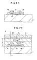
- FIG. 7 illustrates an exemplary conventional thin film magnetic head of such type manufactured by the known method.
- a fore-end electrode 7A and a rear-end electrode 7B are formed to be connected respectively to the fore end and the rear end of the MR element 12, as shown in Fig. 7C.
- an insulator layer 32, a bias conductor 9, an insulator layer 33, an upper shielding magnetic layer 4 and an insulator layer 34 are formed sequentially as shown in Fig. 7D, and then the above structure is polished up to a chained-line position y to thereby produce a thin film magnetic head 11.
- a gap l1 to be finally obtained in the thin film magnetic head 11 is determined by the dimensional sum of the fore-end electrode 7A and the insulator layers 32, 33. Therefore, in the thin film magnetic head having a dual-layer MR element with a bias conductor in particular, a limit exists in the gap l1 with the reliability taken into consideration, and consequently it is difficult to attain a further narrower gap.
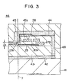
- a lower shielding magnetic layer 42, an insulator layer 431, an MR element 25 and an insulator layer 432 are formed sequentially on a support substrate 41.
- a bias conductor 28 on the insulator layer 432 and a rear-end electrode 27B to be connected to the rear end of the MR element 25 are formed of a conductive material simultaneously with each other.
- the bias conductor 28 and the rear-end electrode 27B may be composed of a high-conductivity material such as Au or Cu, or of the same metallic material as that of an undermentioned fore-end electrode.
- the bias conductor 28 and the rear-end electrode 27B are covered with an insulator layer 433, and patterning is so executed as to simultaneously remove the portions of the insulator layers 433, 432 corresponding to a fore-end gap, thereby forming a fore-end electride 27A to be connected to the fore end of the MR element 25.
- the fore-end electrode 27A is composed of a nonmagnetic moisture-resistant conductor such as Ti, Cr, Mo, W, C or SuS and is connected to an external electrode in an unshown vicinity. And an upper shielding magnetic layer 45 is formed to be electrically connected to the fore-end electrode 27A via a bonding layer 44 composed of a nonmagnetic metal such as Cr. Thereafter the above structure is polished up to a chained-line position y to thereby produce a thin film magnetic head 46.
- a nonmagnetic moisture-resistant conductor such as Ti, Cr, Mo, W, C or SuS
- a lower shielding magnetic layer 42, an insulator layer 431, an MR element 25 and an insulator layer 432 are formed sequentially on a support substrate 41 in a procedure similar to the preceding embodiment, and after the insulator layer 432 is patterned, a bias conductor 28 on the insulator layer 432 and a rear-end electrode 27B to be connected to the rear end of the MR element 25 are composed of the same conductive material simultaneously with each other.
- the bias conductor 28 and the rear-end electrode 27B are covered with an insulator layer 433, and then patterning is so executed as to remove the portions of the insulator layers 432, 433 corresponding to a fore-end gap, thereby forming a fore-end electrode 27A to be connected to the fore end of the MR element 25.
- the fore-end electrode 27A is composed of a nonmagnetic metal to serve also as an undercoat bonding layer for an upper shielding magnetic layer 45.
- This magnetic layer 45 is formed to be electrically connected to the fore-end electrode 27A, and thereafter the above structure is polished up to a chained-line position y to thereby produce a thin film magnetic head 47.
- the upper and lower shielding magnetic layers 45, 42 may be connected to each other as represented by a broken line 48.
- the support substrate 41 may be an insulator substrate or one having an insulator layer on a conductive support member of a suitable material such as Al2O3-Tic shown in Figs 2. Therefore the thin film magnetic heads 46 and 47 of Figs. 3 and 4 may be so constituted as the aforementioned example of Fig. 1 or Fig. 2.
- the gaps l2 and l3 are dimensionally reduced by a length corresponding to the conventional insulator layers 32 and 33 (see Fig. 7D), hence realizing a narrower-gap structure. Since the gap region is formed after completion of the rear-end electrode 27B according to this manufacturing method, the thickness of the rear-end electrode 27B can be rendered sufficiently great to consequently diminish the resistance of the rear-end electrode 27B to a small value, thereby minimizing generation of noise based on the heat from the electrode and hence enhancing the signal-to-noise ratio.
- the problem of interlayer short-circuiting can be solved as the bias conductor 28 is formed simultaneously with the rear-end electrode 27B.
- the resistance value of the electrode material corresponding to such portion is rendered sufficiently small to raise no problem at all.
- the fore-end electrode of the MR element is electrically connected to the shielding magnetic layer, so that the fore end region of the MR element can be electrically stabilized to attain high stability of the characteristics in a playback mode while preventing generation of unsteady noise.
- the first conductor of a great capacity disposed in the proximity of the MR element and the second conductor of a small capacity connected to the fore-end electrode of the MR element are connected to respective ground potentials independently of each other, thereby averting breakdown of the operating thin film magnetic head that may otherwise be caused by the static charge on the surface of a magnetic recording medium.
Landscapes
- Engineering & Computer Science (AREA)
- Manufacturing & Machinery (AREA)
- Magnetic Heads (AREA)
Applications Claiming Priority (2)
| Application Number | Priority Date | Filing Date | Title |
|---|---|---|---|
| JP125852/90 | 1990-05-16 | ||
| JP12585290A JPH0421916A (ja) | 1990-05-16 | 1990-05-16 | 磁気抵抗効果型薄膜ヘッド |
Publications (3)
| Publication Number | Publication Date |
|---|---|
| EP0457278A2 true EP0457278A2 (fr) | 1991-11-21 |
| EP0457278A3 EP0457278A3 (en) | 1992-08-05 |
| EP0457278B1 EP0457278B1 (fr) | 1996-07-17 |
Family
ID=14920538
Family Applications (1)
| Application Number | Title | Priority Date | Filing Date |
|---|---|---|---|
| EP19910107797 Expired - Lifetime EP0457278B1 (fr) | 1990-05-16 | 1991-05-14 | Tête magnétique à film mince à effet de magnétorésistance |
Country Status (3)
| Country | Link |
|---|---|
| EP (1) | EP0457278B1 (fr) |
| JP (1) | JPH0421916A (fr) |
| DE (1) | DE69120866T2 (fr) |
Cited By (11)
| Publication number | Priority date | Publication date | Assignee | Title |
|---|---|---|---|---|
| EP0574896A3 (en) * | 1992-06-17 | 1994-07-13 | Sony Corp | Composite type thin film magnetic head |
| US5375022A (en) * | 1993-08-06 | 1994-12-20 | International Business Machines Corporation | Magnetic disk drive with electrical shorting protection |
| US5465186A (en) * | 1994-01-26 | 1995-11-07 | International Business Machines Corporation | Shorted magnetoresistive head leads for electrical overstress and electrostatic discharge protection during manufacture of a magnetic storage system |
| EP0621584A3 (fr) * | 1993-04-23 | 1996-07-31 | Sony Corp | Tête magnétique à effet de reluctance magnétique. |
| US5557492A (en) * | 1993-08-06 | 1996-09-17 | International Business Machines Corporation | Thin film magnetoresistive head with reduced lead-shield shorting |
| US5973889A (en) * | 1997-02-20 | 1999-10-26 | U.S. Philips Corporation | Single-channel magnetic head with magnetoresistive element in series with electrically conducting magnetic elements |
| WO2000033299A1 (fr) * | 1998-12-02 | 2000-06-08 | International Business Machines Corporation | Tetes magnetoresistantes blindees avec pince de charge |
| EP1022568A1 (fr) * | 1999-01-21 | 2000-07-26 | Philips Patentverwaltung GmbH | Dispositif pour la détermination de la vitesse de rotation |
| US6470566B2 (en) | 2001-01-03 | 2002-10-29 | International Business Machines Corporation | ESD protection during GMR head fabrication |
| US6747854B1 (en) | 1997-02-20 | 2004-06-08 | Koninklijke Philips Electronics N.V. | Multi-channel magnetic head with magnetoresistive elements |
| US6859347B2 (en) | 2001-01-04 | 2005-02-22 | Hitachi Global Storage Technologies Netherlands, B.V. | Magnetic transducer with electrically conductive shield for reducing electromagnetic interference |
Families Citing this family (1)
| Publication number | Priority date | Publication date | Assignee | Title |
|---|---|---|---|---|
| JP3384651B2 (ja) * | 1995-07-17 | 2003-03-10 | 富士通株式会社 | 電源制御回路及び記憶装置 |
Family Cites Families (4)
| Publication number | Priority date | Publication date | Assignee | Title |
|---|---|---|---|---|
| JPS5832221A (ja) * | 1981-08-17 | 1983-02-25 | Sony Corp | 磁気抵抗効果型磁気ヘツド |
| CA1209260A (fr) * | 1982-10-29 | 1986-08-05 | Tetsuo Sekiya | Transducteur magnetique agissant par magnetoresistance |
| DE3604720A1 (de) * | 1985-03-25 | 1986-10-02 | Hitachi, Ltd., Tokio/Tokyo | Magnetwiderstandskopf |
| JPH07105006B2 (ja) * | 1985-11-05 | 1995-11-13 | ソニー株式会社 | 磁気抵抗効果型磁気ヘツド |
-
1990
- 1990-05-16 JP JP12585290A patent/JPH0421916A/ja active Pending
-
1991
- 1991-05-14 EP EP19910107797 patent/EP0457278B1/fr not_active Expired - Lifetime
- 1991-05-14 DE DE1991620866 patent/DE69120866T2/de not_active Expired - Fee Related
Cited By (13)
| Publication number | Priority date | Publication date | Assignee | Title |
|---|---|---|---|---|
| EP0574896A3 (en) * | 1992-06-17 | 1994-07-13 | Sony Corp | Composite type thin film magnetic head |
| US6130810A (en) * | 1993-04-23 | 2000-10-10 | Sony Corporation | Magnetic reluctance effect magnetic head with the connection length of the forward electrode less than the facing length of the magnetic gap |
| EP0621584A3 (fr) * | 1993-04-23 | 1996-07-31 | Sony Corp | Tête magnétique à effet de reluctance magnétique. |
| US5375022A (en) * | 1993-08-06 | 1994-12-20 | International Business Machines Corporation | Magnetic disk drive with electrical shorting protection |
| US5557492A (en) * | 1993-08-06 | 1996-09-17 | International Business Machines Corporation | Thin film magnetoresistive head with reduced lead-shield shorting |
| US5465186A (en) * | 1994-01-26 | 1995-11-07 | International Business Machines Corporation | Shorted magnetoresistive head leads for electrical overstress and electrostatic discharge protection during manufacture of a magnetic storage system |
| US5973889A (en) * | 1997-02-20 | 1999-10-26 | U.S. Philips Corporation | Single-channel magnetic head with magnetoresistive element in series with electrically conducting magnetic elements |
| US6747854B1 (en) | 1997-02-20 | 2004-06-08 | Koninklijke Philips Electronics N.V. | Multi-channel magnetic head with magnetoresistive elements |
| WO2000033299A1 (fr) * | 1998-12-02 | 2000-06-08 | International Business Machines Corporation | Tetes magnetoresistantes blindees avec pince de charge |
| US6246553B1 (en) | 1998-12-02 | 2001-06-12 | International Business Machines Corporation | Shielded magnetoresistive head with charge clamp |
| EP1022568A1 (fr) * | 1999-01-21 | 2000-07-26 | Philips Patentverwaltung GmbH | Dispositif pour la détermination de la vitesse de rotation |
| US6470566B2 (en) | 2001-01-03 | 2002-10-29 | International Business Machines Corporation | ESD protection during GMR head fabrication |
| US6859347B2 (en) | 2001-01-04 | 2005-02-22 | Hitachi Global Storage Technologies Netherlands, B.V. | Magnetic transducer with electrically conductive shield for reducing electromagnetic interference |
Also Published As
| Publication number | Publication date |
|---|---|
| JPH0421916A (ja) | 1992-01-24 |
| DE69120866T2 (de) | 1997-02-20 |
| DE69120866D1 (de) | 1996-08-22 |
| EP0457278B1 (fr) | 1996-07-17 |
| EP0457278A3 (en) | 1992-08-05 |
Similar Documents
| Publication | Publication Date | Title |
|---|---|---|
| US5247413A (en) | Magnetoresistance effect type thin film magnetic head with noise reducing electrode | |
| EP0477941B1 (fr) | Tête magnétique de type à effet magnéto-résistif | |
| EP0682338A2 (fr) | Structure magnétoresistive à conception de polarisation dure à jonction contique, à résistance faible de lignes | |
| US5907459A (en) | Magnetoresistive thin film magnetic head with specific shapes of leads | |
| EP0021392B1 (fr) | Structures de tête transductrice magnétique | |
| EP0459404B1 (fr) | Tête à film mince à effet magnétorésistif | |
| EP0457278B1 (fr) | Tête magnétique à film mince à effet de magnétorésistance | |
| EP0640955A1 (fr) | Assemblage de tête magnétique à structure de pôle d'écriture/écran | |
| US20080259504A1 (en) | Shield biasing for mr devices | |
| JPH05266426A (ja) | 薄膜磁気ヘッド | |
| EP0204902A2 (fr) | Tête de transducteur magnétique du type à culasse utilisant un effet magnétorésistif | |
| TWI417877B (zh) | 具磁阻裝置之遮蔽偏壓之磁性資料儲存系統 | |
| US6671137B2 (en) | Magnetoresistive head including earth members | |
| US5424890A (en) | Magnetoresistance effect type thin film head | |
| JP2731506B2 (ja) | 磁気抵抗効果型磁気ヘッド及びその製造方法 | |
| US5966274A (en) | Magneto-resistive magnetic head with track width defined by oppositely positioned recesses and manufacturing method therefor | |
| JPH064832A (ja) | 複合型薄膜磁気ヘッド | |
| JPH08339514A (ja) | 磁気記録再生装置 | |
| EP0482642A2 (fr) | Tête magnétique composite magnétorésistive à film mince | |
| JP2785413B2 (ja) | 磁気抵抗効果型薄膜ヘッド | |
| JPH06243434A (ja) | 磁気抵抗効果型薄膜磁気ヘッド | |
| JPS61126618A (ja) | 磁気抵抗効果薄膜ヘツド | |
| JP2845450B2 (ja) | 磁気抵抗効果ヘッド | |
| JP2886783B2 (ja) | 磁気抵抗効果型薄膜磁気ヘッド及びその製造方法 | |
| JPS61248212A (ja) | 磁気抵抗効果型ヘツド |
Legal Events
| Date | Code | Title | Description |
|---|---|---|---|
| PUAI | Public reference made under article 153(3) epc to a published international application that has entered the european phase |
Free format text: ORIGINAL CODE: 0009012 |
|
| AK | Designated contracting states |
Kind code of ref document: A2 Designated state(s): DE FR GB |
|
| PUAL | Search report despatched |
Free format text: ORIGINAL CODE: 0009013 |
|
| AK | Designated contracting states |
Kind code of ref document: A3 Designated state(s): DE FR GB |
|
| 17P | Request for examination filed |
Effective date: 19930105 |
|
| 17Q | First examination report despatched |
Effective date: 19941215 |
|
| GRAH | Despatch of communication of intention to grant a patent |
Free format text: ORIGINAL CODE: EPIDOS IGRA |
|
| GRAA | (expected) grant |
Free format text: ORIGINAL CODE: 0009210 |
|
| AK | Designated contracting states |
Kind code of ref document: B1 Designated state(s): DE FR GB |
|
| REF | Corresponds to: |
Ref document number: 69120866 Country of ref document: DE Date of ref document: 19960822 |
|
| ET | Fr: translation filed | ||
| PLBE | No opposition filed within time limit |
Free format text: ORIGINAL CODE: 0009261 |
|
| STAA | Information on the status of an ep patent application or granted ep patent |
Free format text: STATUS: NO OPPOSITION FILED WITHIN TIME LIMIT |
|
| 26N | No opposition filed | ||
| PGFP | Annual fee paid to national office [announced via postgrant information from national office to epo] |
Ref country code: DE Payment date: 20010508 Year of fee payment: 11 |
|
| PGFP | Annual fee paid to national office [announced via postgrant information from national office to epo] |
Ref country code: GB Payment date: 20010509 Year of fee payment: 11 |
|
| PGFP | Annual fee paid to national office [announced via postgrant information from national office to epo] |
Ref country code: FR Payment date: 20010518 Year of fee payment: 11 |
|
| REG | Reference to a national code |
Ref country code: GB Ref legal event code: IF02 |
|
| PG25 | Lapsed in a contracting state [announced via postgrant information from national office to epo] |
Ref country code: GB Free format text: LAPSE BECAUSE OF NON-PAYMENT OF DUE FEES Effective date: 20020514 |
|
| PG25 | Lapsed in a contracting state [announced via postgrant information from national office to epo] |
Ref country code: DE Free format text: LAPSE BECAUSE OF NON-PAYMENT OF DUE FEES Effective date: 20021203 |
|
| GBPC | Gb: european patent ceased through non-payment of renewal fee |
Effective date: 20020514 |
|
| PG25 | Lapsed in a contracting state [announced via postgrant information from national office to epo] |
Ref country code: FR Free format text: LAPSE BECAUSE OF NON-PAYMENT OF DUE FEES Effective date: 20030131 |
|
| REG | Reference to a national code |
Ref country code: FR Ref legal event code: ST |