EP0457373A2 - Verzögerungsverfahren für ein Informationssignal - Google Patents
Verzögerungsverfahren für ein Informationssignal Download PDFInfo
- Publication number
- EP0457373A2 EP0457373A2 EP91113171A EP91113171A EP0457373A2 EP 0457373 A2 EP0457373 A2 EP 0457373A2 EP 91113171 A EP91113171 A EP 91113171A EP 91113171 A EP91113171 A EP 91113171A EP 0457373 A2 EP0457373 A2 EP 0457373A2
- Authority
- EP
- European Patent Office
- Prior art keywords
- signal
- information
- memory
- recording apparatus
- delayed
- Prior art date
- Legal status (The legal status is an assumption and is not a legal conclusion. Google has not performed a legal analysis and makes no representation as to the accuracy of the status listed.)
- Withdrawn
Links
- 230000015654 memory Effects 0.000 claims abstract description 54
- 230000003111 delayed effect Effects 0.000 claims abstract description 26
- 230000003466 anti-cipated effect Effects 0.000 abstract 1
- 230000006835 compression Effects 0.000 abstract 1
- 238000007906 compression Methods 0.000 abstract 1
- 230000035484 reaction time Effects 0.000 abstract 1
- 230000005236 sound signal Effects 0.000 description 18
- 238000010586 diagram Methods 0.000 description 5
- 230000007246 mechanism Effects 0.000 description 5
- 238000006243 chemical reaction Methods 0.000 description 4
- 230000005540 biological transmission Effects 0.000 description 3
- 238000005516 engineering process Methods 0.000 description 3
- 240000007320 Pinus strobus Species 0.000 description 2
- 230000001934 delay Effects 0.000 description 2
- 230000006870 function Effects 0.000 description 2
- 238000000034 method Methods 0.000 description 2
- 230000004044 response Effects 0.000 description 2
- 230000000630 rising effect Effects 0.000 description 2
- 239000004065 semiconductor Substances 0.000 description 2
- 230000001960 triggered effect Effects 0.000 description 2
- 230000003044 adaptive effect Effects 0.000 description 1
- 230000008859 change Effects 0.000 description 1
- 239000013078 crystal Substances 0.000 description 1
- 238000012544 monitoring process Methods 0.000 description 1
- 230000036316 preload Effects 0.000 description 1
- 230000008569 process Effects 0.000 description 1
- 230000000644 propagated effect Effects 0.000 description 1
- 230000000717 retained effect Effects 0.000 description 1
- 230000001360 synchronised effect Effects 0.000 description 1
- 230000002194 synthesizing effect Effects 0.000 description 1
- 230000007723 transport mechanism Effects 0.000 description 1
Images


Classifications
-
- G—PHYSICS
- G11—INFORMATION STORAGE
- G11B—INFORMATION STORAGE BASED ON RELATIVE MOVEMENT BETWEEN RECORD CARRIER AND TRANSDUCER
- G11B20/00—Signal processing not specific to the method of recording or reproducing; Circuits therefor
- G11B20/02—Analogue recording or reproducing
-
- G—PHYSICS
- G11—INFORMATION STORAGE
- G11B—INFORMATION STORAGE BASED ON RELATIVE MOVEMENT BETWEEN RECORD CARRIER AND TRANSDUCER
- G11B15/00—Driving, starting or stopping record carriers of filamentary or web form; Driving both such record carriers and heads; Guiding such record carriers or containers therefor; Control thereof; Control of operating function
- G11B15/02—Control of operating function, e.g. switching from recording to reproducing
-
- G—PHYSICS
- G11—INFORMATION STORAGE
- G11B—INFORMATION STORAGE BASED ON RELATIVE MOVEMENT BETWEEN RECORD CARRIER AND TRANSDUCER
- G11B20/00—Signal processing not specific to the method of recording or reproducing; Circuits therefor
-
- G—PHYSICS
- G11—INFORMATION STORAGE
- G11B—INFORMATION STORAGE BASED ON RELATIVE MOVEMENT BETWEEN RECORD CARRIER AND TRANSDUCER
- G11B20/00—Signal processing not specific to the method of recording or reproducing; Circuits therefor
- G11B20/00007—Time or data compression or expansion
-
- G—PHYSICS
- G11—INFORMATION STORAGE
- G11B—INFORMATION STORAGE BASED ON RELATIVE MOVEMENT BETWEEN RECORD CARRIER AND TRANSDUCER
- G11B27/00—Editing; Indexing; Addressing; Timing or synchronising; Monitoring; Measuring tape travel
- G11B27/02—Editing, e.g. varying the order of information signals recorded on, or reproduced from, record carriers
- G11B27/022—Electronic editing of analogue information signals, e.g. audio or video signals
- G11B27/029—Insert-editing
-
- G—PHYSICS
- G11—INFORMATION STORAGE
- G11B—INFORMATION STORAGE BASED ON RELATIVE MOVEMENT BETWEEN RECORD CARRIER AND TRANSDUCER
- G11B27/00—Editing; Indexing; Addressing; Timing or synchronising; Monitoring; Measuring tape travel
- G11B27/02—Editing, e.g. varying the order of information signals recorded on, or reproduced from, record carriers
- G11B27/031—Electronic editing of digitised analogue information signals, e.g. audio or video signals
- G11B27/036—Insert-editing
-
- G—PHYSICS
- G11—INFORMATION STORAGE
- G11C—STATIC STORES
- G11C7/00—Arrangements for writing information into, or reading information out from, a digital store
-
- G—PHYSICS
- G11—INFORMATION STORAGE
- G11C—STATIC STORES
- G11C7/00—Arrangements for writing information into, or reading information out from, a digital store
- G11C7/16—Storage of analogue signals in digital stores using an arrangement comprising analogue/digital [A/D] converters, digital memories and digital/analogue [D/A] converters
-
- G—PHYSICS
- G11—INFORMATION STORAGE
- G11B—INFORMATION STORAGE BASED ON RELATIVE MOVEMENT BETWEEN RECORD CARRIER AND TRANSDUCER
- G11B2220/00—Record carriers by type
- G11B2220/40—Combinations of multiple record carriers
- G11B2220/45—Hierarchical combination of record carriers, e.g. HDD for fast access, optical discs for long term storage or tapes for backup
- G11B2220/455—Hierarchical combination of record carriers, e.g. HDD for fast access, optical discs for long term storage or tapes for backup said record carriers being in one device and being used as primary and secondary/backup media, e.g. HDD-DVD combo device, or as source and target media, e.g. PC and portable player
-
- G—PHYSICS
- G11—INFORMATION STORAGE
- G11B—INFORMATION STORAGE BASED ON RELATIVE MOVEMENT BETWEEN RECORD CARRIER AND TRANSDUCER
- G11B2220/00—Record carriers by type
- G11B2220/90—Tape-like record carriers
-
- G—PHYSICS
- G11—INFORMATION STORAGE
- G11C—STATIC STORES
- G11C2207/00—Indexing scheme relating to arrangements for writing information into, or reading information out from, a digital store
- G11C2207/16—Solid state audio
Definitions
- the present invention is directed to the delay of real-time information signals, such as audio or video signals and is particularly concerned with the selective, human responsive recording of such information signals.
- US 4125865 describes a recording system which includes a microphone, a recording apparatus and a time delay device which includes an analog-to-digital converter and means for delaying a digital signal.
- the means for delaying may be in the form of a shift register or a random access memory.
- This recording system is used to record sounds within a predetermined volume range and may be used as an automatic dictation recorder.
- the time delay mechanism is only required to ensure that the initial sound which starts the recording mechanism is itself recorded and since recording is actuated automatically the actual time delay required is of the order of 100 milliseconds.
- GB-A-2081057 describes a digitized signal recording and playback system having means of compressing a digital signal to be stored in a memory and means of expanding said signal read out of said memory in order to avoid memory capacity problems when storing an audio signal converted into a digital signal.
- the present invention provides an information recording apparatus including: means for receiving an information signal; a memory unit having a plurality of addressable storage locations for temporarily storing the information signal; means for controlling the memory unit to continually store the information signal in a sequential manner in each of said storage locations and to continually read out the stored signal a predetermined time period after storage at each location to produce a delayed signal; means for receiving the delayed signal read from said memory unit and feeding continually said delayed signal to a recording device; characterized in that said recording apparatus includes means for controlling the recording device to selectively record only desired portions of the delayed signal based on the content of the information signal.
- the present application is a divisional of European patent application, No. 86304307.1 which describes and claims audio tape recorder apparatus including: a microphone for receiving an audio signal and producing an electrical signal related thereto; an analog-to-digital converter for receiving said electrical signal and producing a digital signal having a predetermined number of bits; a memory unit having a plurality of addressable storage locations for storing the digital signal; means for controlling said memory unit to continually store the digital signal in a sequential manner in each of said storage locations and to continually read out the stored signal a predetermined time period after storage at each location; means for receiving the stored signal read from said memory; and means for synthesizing the stored signal received to produce an audio output signal and for feeding said audio output signal to a tape recorder; characterised in that said audio tape recorder apparatus further includes means for enabling manual control of the audio tape recorder apparatus and means for compressing the digital signal from said analog-to-digital converter into a format having a smaller number of bits, the compressed digital signal being stored in said storage locations of said memory unit, said means for receiving
- a delayed audio signal can be used in environments other than where it is desired to selectively record information.
- the general principles underlying the present invention are not limited to the delay of audio signals, but can be applied to any type of information signal in either an analog or digital form.
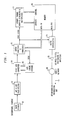
- the real-time information is entered into a selective recording system by means of an input element 10.
- the input element can be any suitable conventional type of condenser microphone typically found in tape recorders.
- the input element 10 can be any suitable type of video camera.
- the information signal from the input element is amplified to a suitable level and filtered to remove unwanted frequencies in an AGC and low pass filter circuit 12, and then presented to an analog-to-digital (A/D) converter 14. In the converter, the analog information signal is transformed into an 8-bit digital signal for storage purposes.
- the digital signal can first be compressed.
- the 8-bit signal from the converter 14 is presented to an adaptive differential pulse code modulator (ADPCM) analyzer.
- ADPCM adaptive differential pulse code modulator
- This analyzer performs a mathematical algorithm which compresses the 8-bit data into a 4-bit format.
- the analyzer generates a control signal SCON that is fed to a timing control circuit 18 to synchronize the output of digital information from the converter 14 with the operation of the analyzer 16.
- the four-bit data that is produced by the analyzer 16 is fed to memory unit 20.
- This memory unit is preferably a solid-state random access memory. However, it could be comprised of other types of addressable memories, such as a hard magnetic disk or a line-addressable CCD array.
- a memory timing and address generator circuit 22 that is responsive to a synchronization clock signal generated by the analyzer 16 the four-bit data is fed into sequential address locations within the memory 20. Also under control of the timing and address generator circuit 22, the stored data is subsequently read out of the memory 20 and fed to an ADPCM synthesizer 24.
- the timing and address generator circuit 22 sequentially addresses each successive storage location in the memory device 20. During the time that each location is addressed, the timing circuit 22 generates two control signals. The first control signal is a read signal which causes the information stored at the address location to be retrieved from that location and read out of the memory for presentation to the synthesizer 24. Subsequently, while that storage location is still being addressed, a write signal is generated to cause the next piece of information from the analyzer 16 to be stored in the memory at that location. Once these successive reading and writing operations have been carried out for the address location, the timing and address generator circuit 22 then generates the address for the next successive location in the memory.
- the first control signal is a read signal which causes the information stored at the address location to be retrieved from that location and read out of the memory for presentation to the synthesizer 24.
- a write signal is generated to cause the next piece of information from the analyzer 16 to be stored in the memory at that location.
- the address generator 22 continuously cycles through each storage location in the memory in succession, so that a given piece of information from the analyzer 16 is written into a storage location on one cycle and then retrieved from that location on the next cycle. Accordingly, the digital signal that is presented to the synthesizer 24 is delayed, relative to the time that it was fed into the memory 20, by the amount of time that it takes the address generator to cycle through the storage locations in the memory.
- the time delay between reading the information into the memory and subsequently retrieving it can be varied by changing the number of addressable locations in the memory or by varying the speed at which they are addressed.
- the address generator 22 is programmable so that different numbers of addressable locations in the memory can be selectively utilized in accordance with different desired time delays.
- the delayed digital information that is retrieved from the memory 20 and presented to the synthesizer 24 is re-converted into an analog information signal, again using conventional algorithms.
- This analog signal can be smoothed and filtered in a low pass filter, integrator and amplifier network 26 Due to the conversion process that is carried out in the synthesizer 24, a sub-carrier might be introduced into the information signal.
- This sub-carrier can be removed in a twin-T filter network 29 which shunts the unwanted carrier frequency to ground.
- the information signal that is produced by the twin-T filter network is a substantially exact replica of the input signal presented to the input element 10, but delayed by the cycle time of the memory 20.
- This delayed information signal can be fed to a conventional recording mechanism, e.g. a magnetic tape recorder.
- the selective recording of this information can be carried out by controlling the recorder in a conventional fashion. For example, if a magnetic tape recorder is employed, the tape transport mechanism can be selectively actuated to record only the desired information. Even though the information is continuously applied to the recorder, it will not be recorded during those periods of time when the recorder is disabled. Accordingly, the system enables real-time information to be selectively recorded without any loss due to the normal response time of the observer.
- the delay system illustrated in Figure 1 could be integrated within a conventional recording mechanism, or it could be separate structural element that is attached to the remote input terminal of the recorder.
- the audio output signal from the microphone 10 is fed in parallel to a plurality of transmission gates 30 configured as a two-line demultiplexer. These gates, under control of a feedback signal, selectively permit the audio signal to pass through to a 3-stage amplifier and low-pass filter network 32.
- the amplified and filtered output signal from the network 32 forms the feedback signal which controls the transmission gates 30.
- the transmission gates are selectively turned on and off in response to the amplitude of the amplified audio signal, thereby performing an automatic gain control function through limitation of the maximum amplitude signal that is passed on to the amplifiers.
- the amplified and filtered audio signal is also fed to an analog-to-digital converter 34.
- the A/D converter 34 produces a parallel eight-bit output signal which is applied to a parallel-to-serial (P/S) shift register 36 to convert the digital signal to a serial format.
- P/S parallel-to-serial
- the 8-bit serial, digitized audio signal ADSI is then presented to an ADPCM analyzer 38.
- This analyzer could be type MSM 5218RS sold by OKI Semiconductor, Inc., for example.
- the analyzer compresses the 8-bit input signal into a 4-bit format which appears in parallel on the data output lines D0-D3. This 4-bit data signal is applied to data input terminals of a RAM memory device 40.
- the analyzer 38 In addition to producing the 4-bit data signals, the analyzer 38 also generates various control signals.
- a start conversion timing signal SCON is applied to the read and write input terminals of the A/D converter 34 and the SHIFT/ LOAD control terminal of the P/S shift register to synchronize the conversion of the audio signal and feeding of information with the operation of the analyzer.
- the SCON signal When the SCON signal is in one logic state, e.g. zero, the A/D converter 34 generates eight bits of data that are loaded into the shift register 36.
- the SCON signal When the SCON signal is in the other state the data is shifted out of the register and into the analyzer 38.
- the change of state of the SCON signal triggers a J-K flip-flop 42, causing its Q (true) output signal to go to a logic one.
- This signal enables a NAND gate 44, allowing a clock signal generated by a crystal oscillator 46 to be passed through to an inverter 48 and presented as a SHIFT strobe to the trigger input of the register 36.
- These pulses are also inverted and presented to the analyzer 38 as a shift clock signal (SICLK) by means of a NAND gate 49 that is enabled by the SCON signal.
- SICLK shift clock signal
- the Q (false) output terminal of the flip-flop 42 goes to a logic zero.
- This signal allows a 4-bit binary counter 50 to begin counting clock pulses. When the counter has reached a count of 12, it sends a reset signal to clear the flip-flop 42. This terminates the shift clock signal that is presented to the register 36 and the analyzer 38. When the Q (false) output signal goes to a logic one upon clearing the flip-flop 42, the counter 50 is pulsed, which pre-loads it with a count of two for the next cycle.
- a second timing signal, VCLK, is synchronized with the output of information from the analyzer. This signal is applied to the timing and address generator circuit 22 to control the reading of information into the memory device 40.
- the 4-bit ADPCM data from the analyzer 38 is applied to the data input terminals of the memory unit 40.
- the VCLK signal is directly applied to one input terminal of an exclusive-OR gate 52 and is delayed in an RC delay circuit 54 and presented to another exclusive-OR gate 56.
- the two exclusive-OR gates and the delay circuit form a negative pulse generator which is triggered on both the rising and falling edges of the VCLK signal. These pulses (NEG) are applied to a negative-edge triggered flip-flop 58.
- a logic zero signal is fed to the J-K inputs of a 4-bit parallel-in parallel-out shift register 60 whose data input terminals are all tied to a constant voltage reference.
- the logic signals appearing at the output terminals of the register 60 control the reading and writing of information in the memory 40. Data appears at the input terminals of the memory at the falling edge of the VCLK signal.
- a row address signal RAS is strobed into the memory.
- the column address is strobed when the Q4 output terminal goes to a logic zero.
- the actual row and column addresses are generated by a pair or cascaded 8-bit counters 62. These counters form a 16-bit address signal that is multiplexed by a pair of 8:4 multiplexers 64.
- MUX Q2 output terminal
- the column address is presented to the memory, and is strobed in when the CAS signal from the Q4 output terminal goes to zero.
- the signal WR from the Q3 output terminal of the register 60 is used to provide a write pulse which strobes data into the memory.
- This signal is applied to one input terminal of an exclusive-OR gate 66 whose other input terminal is at a fixed logic level, e.g. one.
- the output signal from this gate is applied to one input terminal of a NAND gate 68.
- the VCLK signal is applied to one input terminal of an exclusive-OR gate 70 which functions to invert this signal.
- the inverted signal is applied to the other input terminal of the NAND gate 68 as well as one of the cascaded counters 62.
- the combination of gates 66, 68 and 70 is equivalent to an OR gate, so that an inverted write pulse WRG is applied to the memory 40 only when both the VCLK signal and the WR output signal are a logic zero.
- the VCLK signal goes to a logic zero and three shift clock pulses later the WR output signal of the register 60 goes to zero.
- the write pulse is applied to the memory to begin a write cycle.
- This pulse remains for four more shift clock pulses and then terminates even though the VCLK signal remains low.
- the address generator counters 62 then advance one count on the rising edge of the column address signal CAS when the VCLK signal is a logic zero, to begin a read cycle.
- the sequence of operations is the same as a write cycle, except that the write pulse is not applied to the memory because the VCLK signal is a logic one.
- the read cycle causes data to be presented at the output terminals of the memory, where it is fed to the synthesizer 24 to be converted into a delayed audio signal.
- the length of the delay period is related to the number of locations that are used in the memory as well as the speed with which they are accessed. For example, if 64K 4-bit memory locations are loaded using a VCLK signal having a frequency of 8KHz, the signal will be delayed by about 8 seconds.
- the resynthesized audio signal passes through a twin-T network 72 and a low pass filter 74 to smooth it and remove unwanted noise.
- This signal is then fed to an FET 76 which is configured as a self-biasing impedance matching device to enable it to be applied to different types of recorders.
- the present invention provides an effective means for utilizing state of the art memory technology to delay a real-time information signal.
- the practical applications of the invention are not so limited. Rather, it can be used with any type of information signal that is in a digital form, or is capable of being digitised and subsequently reconverted to its original form.
- a digital video signal obtained from a CCD array can be directly stored in a RAM and later retrieved without the need for initial analog-to-digital conversion.
- both video and audio signals can be concurrently delayed using the techniques of the present invention to provide selective recording of an event on a video cassette recorder.
- the delay mechanism could be incorporated in the structure of the recorder itself, or it could be a separate element that receives and delays the information signals prior to presentation to the recorder.
Landscapes
- Engineering & Computer Science (AREA)
- Signal Processing (AREA)
- Multimedia (AREA)
- Signal Processing For Digital Recording And Reproducing (AREA)
- Synchronisation In Digital Transmission Systems (AREA)
- Reduction Or Emphasis Of Bandwidth Of Signals (AREA)
- Electrophonic Musical Instruments (AREA)
- Stereo-Broadcasting Methods (AREA)
- Television Systems (AREA)
Applications Claiming Priority (2)
| Application Number | Priority Date | Filing Date | Title |
|---|---|---|---|
| US06/741,941 US4633331A (en) | 1985-06-06 | 1985-06-06 | Information signal delay system utilizing random access memory |
| US741941 | 2000-12-21 |
Related Parent Applications (1)
| Application Number | Title | Priority Date | Filing Date |
|---|---|---|---|
| EP86304307.1 Division | 1986-06-05 |
Publications (2)
| Publication Number | Publication Date |
|---|---|
| EP0457373A2 true EP0457373A2 (de) | 1991-11-21 |
| EP0457373A3 EP0457373A3 (en) | 1992-01-29 |
Family
ID=24982867
Family Applications (2)
| Application Number | Title | Priority Date | Filing Date |
|---|---|---|---|
| EP86304307A Expired EP0204578B1 (de) | 1985-06-06 | 1986-06-05 | Verzögerungsverfahren für ein Informationssignal |
| EP19910113171 Withdrawn EP0457373A3 (en) | 1985-06-06 | 1986-06-05 | An information signal delay system |
Family Applications Before (1)
| Application Number | Title | Priority Date | Filing Date |
|---|---|---|---|
| EP86304307A Expired EP0204578B1 (de) | 1985-06-06 | 1986-06-05 | Verzögerungsverfahren für ein Informationssignal |
Country Status (4)
| Country | Link |
|---|---|
| US (1) | US4633331A (de) |
| EP (2) | EP0204578B1 (de) |
| AT (1) | ATE73567T1 (de) |
| DE (1) | DE3684177D1 (de) |
Cited By (2)
| Publication number | Priority date | Publication date | Assignee | Title |
|---|---|---|---|---|
| FR2700908A1 (fr) * | 1993-01-26 | 1994-07-29 | Thomson Consumer Electronics | Récepteur de télévision à mémoire tampon. |
| EP1057171A4 (de) * | 1998-01-22 | 2006-09-20 | Henry C Yuen | Audiorecorder mit rückgekoppeltem speicher |
Families Citing this family (53)
| Publication number | Priority date | Publication date | Assignee | Title |
|---|---|---|---|---|
| FR2606922A1 (fr) * | 1986-11-14 | 1988-05-20 | Meflah Abdelkader | Dispositif enregistreur permanent d'evenements passes |
| KR930009531B1 (ko) * | 1987-01-07 | 1993-10-06 | 상요 덴기 가부시기가이샤 | 신호 기록 장치 |
| JPH0738120B2 (ja) * | 1987-07-14 | 1995-04-26 | 三菱電機株式会社 | 音声記録再生装置 |
| US4943865A (en) * | 1987-10-08 | 1990-07-24 | The Boeing Company | Method and system for recording standard pulse code modulated serial data using video signal recorders |
| JP3004018B2 (ja) * | 1987-12-15 | 2000-01-31 | 株式会社東芝 | 信号記録装置 |
| FR2633132B1 (fr) * | 1988-06-17 | 1993-11-12 | Ulmer Siegfried | Procede et dispositif pour eliminer les seances publicitaires d'une emission de television |
| US5450146A (en) * | 1989-05-24 | 1995-09-12 | Digital Theater Systems, L.P. | High fidelity reproduction device for cinema sound |
| DE3921942A1 (de) * | 1989-07-04 | 1991-01-17 | Grundig Emv | Schaltungsanordnung zur ueberarbeitung eines in einem magnetband- und/oder halbleiterspeicher abgespeicherten gesprochenen textes |
| US5126982A (en) * | 1990-09-10 | 1992-06-30 | Aaron Yifrach | Radio receiver and buffer system therefore |
| US5241428A (en) * | 1991-03-12 | 1993-08-31 | Goldwasser Eric P | Variable-delay video recorder |
| WO1992021211A1 (en) * | 1991-05-21 | 1992-11-26 | Videotelecom Corp. | A multiple medium message recording system |
| FR2679090A1 (fr) * | 1991-07-08 | 1993-01-15 | Sgs Thomson Microelectronics | Recepteur a memoire remanente. |
| DE4229710B4 (de) * | 1991-09-09 | 2008-06-05 | Samsung Electronics Co., Ltd. | Digitales Audiodatenspeicherungssystem und damit ausgerüstetes digitales Audio-System |
| JPH0589407A (ja) * | 1991-09-30 | 1993-04-09 | Pioneer Electron Corp | テープレコーダの再生方式および録音方式 |
| FR2684463A1 (fr) * | 1991-12-03 | 1993-06-04 | Lochen Elisabeth | Dispositif haute fidelite de reproduction du son au cinema. |
| GB2262826A (en) * | 1991-12-09 | 1993-06-30 | And Electronics Co Ltd | Sound recording/playing device. |
| JP3071946B2 (ja) * | 1992-06-09 | 2000-07-31 | 株式会社日立製作所 | 磁気記録再生信号の処理回路およびそれを用いた記録再生装置 |
| US5329320A (en) * | 1992-12-03 | 1994-07-12 | Aharon Yifrach | TV receiver and buffer system therefor |
| US5701383A (en) * | 1994-05-20 | 1997-12-23 | Gemstar Development Corporation | Video time-shifting apparatus |
| JP3560074B2 (ja) * | 1994-07-29 | 2004-09-02 | ソニー株式会社 | 記録再生装置、及びメモリ制御装置 |
| US5463599A (en) * | 1994-08-23 | 1995-10-31 | Yifrach; Aharon | Radio receiver and buffer system therefor |
| US6035367A (en) * | 1997-04-04 | 2000-03-07 | Avid Technology, Inc. | Computer file system providing looped file structure for post-occurrence data collection of asynchronous events |
| GB2325547B (en) * | 1997-05-23 | 2000-04-19 | Texas Instruments Ltd | Improvements in or relating to data communications |
| IL125141A0 (en) | 1998-06-29 | 1999-01-26 | Nds Ltd | Advanced television system |
| IL121230A (en) | 1997-07-03 | 2004-05-12 | Nds Ltd | Intelligent electronic program guide |
| US6788882B1 (en) | 1998-04-17 | 2004-09-07 | Timesurf, L.L.C. | Systems and methods for storing a plurality of video streams on re-writable random-access media and time-and channel- based retrieval thereof |
| US7272298B1 (en) | 1998-05-06 | 2007-09-18 | Burst.Com, Inc. | System and method for time-shifted program viewing |
| US8577205B2 (en) | 1998-07-30 | 2013-11-05 | Tivo Inc. | Digital video recording system |
| US6233389B1 (en) | 1998-07-30 | 2001-05-15 | Tivo, Inc. | Multimedia time warping system |
| US8380041B2 (en) | 1998-07-30 | 2013-02-19 | Tivo Inc. | Transportable digital video recorder system |
| US7558472B2 (en) | 2000-08-22 | 2009-07-07 | Tivo Inc. | Multimedia signal processing system |
| US6324338B1 (en) | 1998-08-07 | 2001-11-27 | Replaytv, Inc. | Video data recorder with integrated channel guides |
| US20020054752A1 (en) | 1998-08-07 | 2002-05-09 | Anthony Wood | Video data recorder with personal channels |
| US20040260415A1 (en) * | 1999-09-08 | 2004-12-23 | Weiss Kenneth P. | Method and apparatus for achieving selected audio and other functions |
| US20090322953A1 (en) * | 1999-09-08 | 2009-12-31 | Weiss Kenneth P | Method and apparatus for achieving selected audio/video and other functions |
| US6647479B1 (en) * | 2000-01-03 | 2003-11-11 | Avid Technology, Inc. | Computer file system providing looped file structure for post-occurrence data collection of asynchronous events |
| US20060259926A1 (en) | 2000-07-20 | 2006-11-16 | Digital Deck, Inc. | Adaptable programming guide for networked devices |
| US20020029384A1 (en) | 2000-07-20 | 2002-03-07 | Griggs Theodore L. | Mechanism for distributing content data |
| DE10225623A1 (de) * | 2002-06-07 | 2003-12-18 | Bosch Gmbh Robert | Verfahren zur Aufzeichnung über Funk, insbesondere Rundfunk, empfangener Informationen, insbesondere Audiosignale |
| JP3915705B2 (ja) * | 2003-01-30 | 2007-05-16 | 松下電器産業株式会社 | 磁気記録再生装置 |
| CN101077006A (zh) | 2004-11-19 | 2007-11-21 | Tivo股份有限公司 | 用于先前播放内容的安全传输的方法和设备 |
| US8165450B2 (en) | 2007-11-19 | 2012-04-24 | Echostar Technologies L.L.C. | Methods and apparatus for filtering content in a video stream using text data |
| US8136140B2 (en) | 2007-11-20 | 2012-03-13 | Dish Network L.L.C. | Methods and apparatus for generating metadata utilized to filter content from a video stream using text data |
| US8165451B2 (en) | 2007-11-20 | 2012-04-24 | Echostar Technologies L.L.C. | Methods and apparatus for displaying information regarding interstitials of a video stream |
| US8606085B2 (en) | 2008-03-20 | 2013-12-10 | Dish Network L.L.C. | Method and apparatus for replacement of audio data in recorded audio/video stream |
| US8156520B2 (en) | 2008-05-30 | 2012-04-10 | EchoStar Technologies, L.L.C. | Methods and apparatus for presenting substitute content in an audio/video stream using text data |
| US8510771B2 (en) | 2008-12-24 | 2013-08-13 | Echostar Technologies L.L.C. | Methods and apparatus for filtering content from a presentation stream using signature data |
| US8588579B2 (en) | 2008-12-24 | 2013-11-19 | Echostar Technologies L.L.C. | Methods and apparatus for filtering and inserting content into a presentation stream using signature data |
| US8407735B2 (en) | 2008-12-24 | 2013-03-26 | Echostar Technologies L.L.C. | Methods and apparatus for identifying segments of content in a presentation stream using signature data |
| US8437617B2 (en) | 2009-06-17 | 2013-05-07 | Echostar Technologies L.L.C. | Method and apparatus for modifying the presentation of content |
| US8934758B2 (en) | 2010-02-09 | 2015-01-13 | Echostar Global B.V. | Methods and apparatus for presenting supplemental content in association with recorded content |
| US9743125B2 (en) | 2012-07-03 | 2017-08-22 | Trimvid, Llc. | System and method for visual editing |
| US11172269B2 (en) | 2020-03-04 | 2021-11-09 | Dish Network L.L.C. | Automated commercial content shifting in a video streaming system |
Family Cites Families (13)
| Publication number | Priority date | Publication date | Assignee | Title |
|---|---|---|---|---|
| US3028454A (en) * | 1959-04-20 | 1962-04-03 | Kohorn Henry Von | Selective recording of continuous information |
| US3921209A (en) * | 1971-06-18 | 1975-11-18 | Matsushita Electric Industrial Co Ltd | Digital recording and reproducing system employing ' pcm |
| US3812530A (en) * | 1972-12-18 | 1974-05-21 | Konan Camera Res Inst | Magnetic recording appliance with control for transferring desired information from an endless tape |
| US4125865A (en) * | 1977-01-03 | 1978-11-14 | Lanier Business Products, Inc. | Recording system |
| US4321460A (en) * | 1977-01-03 | 1982-03-23 | Lanier Business Products, Inc. | Digital control apparatus |
| DE2826870A1 (de) * | 1978-06-19 | 1980-01-03 | Siemens Ag | Halbleitergeraet zur reproduktion akustischer signale |
| US4348754A (en) * | 1980-05-15 | 1982-09-07 | Ampex Corporation | Digital delay for high quality audio use |
| US4363050A (en) * | 1980-07-28 | 1982-12-07 | Rca Corporation | Digitized audio record and playback system |
| US4408309A (en) * | 1981-07-20 | 1983-10-04 | Kiesling Roy A | Time delayed recording system |
| US4528689A (en) * | 1981-09-22 | 1985-07-09 | International Acoustics Incorporated | Sound monitoring apparatus |
| JPS58208914A (ja) * | 1982-05-31 | 1983-12-05 | Toshiba Ii M I Kk | オーディオ用記録媒体の記録再生装置およびそれに使用する記録媒体 |
| JPS58218010A (ja) * | 1982-06-10 | 1983-12-19 | Victor Co Of Japan Ltd | 信号の符号化記憶再生装置 |
| FR2580422B1 (fr) * | 1985-04-12 | 1988-08-19 | Inst Nat Sante Rech Med | Dispositif electronique de memorisation de signaux audio et de restitution audible commandee, retardee ou differee des signaux memorises |
-
1985
- 1985-06-06 US US06/741,941 patent/US4633331A/en not_active Expired - Lifetime
-
1986
- 1986-06-05 AT AT86304307T patent/ATE73567T1/de not_active IP Right Cessation
- 1986-06-05 EP EP86304307A patent/EP0204578B1/de not_active Expired
- 1986-06-05 EP EP19910113171 patent/EP0457373A3/en not_active Withdrawn
- 1986-06-05 DE DE8686304307T patent/DE3684177D1/de not_active Expired - Fee Related
Cited By (2)
| Publication number | Priority date | Publication date | Assignee | Title |
|---|---|---|---|---|
| FR2700908A1 (fr) * | 1993-01-26 | 1994-07-29 | Thomson Consumer Electronics | Récepteur de télévision à mémoire tampon. |
| EP1057171A4 (de) * | 1998-01-22 | 2006-09-20 | Henry C Yuen | Audiorecorder mit rückgekoppeltem speicher |
Also Published As
| Publication number | Publication date |
|---|---|
| US4633331A (en) | 1986-12-30 |
| EP0204578A2 (de) | 1986-12-10 |
| EP0204578B1 (de) | 1992-03-11 |
| EP0204578A3 (en) | 1987-01-28 |
| ATE73567T1 (de) | 1992-03-15 |
| EP0457373A3 (en) | 1992-01-29 |
| DE3684177D1 (de) | 1992-04-16 |
Similar Documents
| Publication | Publication Date | Title |
|---|---|---|
| EP0204578B1 (de) | Verzögerungsverfahren für ein Informationssignal | |
| US6058236A (en) | System and method for digitally capturing video segments from a video assist of a film camera | |
| JPS5933605A (ja) | 電子スチルカメラの音声記録方式 | |
| US3803363A (en) | Apparatus for the modification of the time duration of waveforms | |
| KR20000029500A (ko) | 연속기록된데이터의선택적재호출및보존 | |
| EP0691648A4 (de) | Informationsdatenaufzeichnungs- und wiedergabevorrichtung und informationsdatenverarbeitungssystem | |
| US4591929A (en) | Interactive learning programming and like control circuitry | |
| US4301480A (en) | Apparatus for monitoring reproduced audio signals during fast playback operation | |
| US6678461B1 (en) | Media recorder for capture and playback of live and prerecorded audio and/or video information | |
| JPS62243490A (ja) | ビデオ編集および処理方法および装置 | |
| JPH0244502A (ja) | 磁気記録・再生装置 | |
| US20010022893A1 (en) | Digital audio/video disk recorder with pre-record function | |
| EP0702354A1 (de) | Vorrichtung zur Modifizierung der Modifikation der Sprachzeitskala | |
| US3838218A (en) | Bifrequency controlled analog shift register speech processor | |
| US5841945A (en) | Voice signal compacting and expanding device with frequency division | |
| JP3505208B2 (ja) | 音声再生装置 | |
| JPH087595B2 (ja) | 音声信号再生装置 | |
| JPS6124059A (ja) | Pcm音声再生装置 | |
| JPS5897171A (ja) | 電子編集の編集点検出回路 | |
| JPH0458640B2 (de) | ||
| JPH02143955A (ja) | データ記録再生装置 | |
| JPS5612181A (en) | Signal recording and reproducing device | |
| JPH05303400A (ja) | 音声再生装置と音声再生方法 | |
| JPS5945607A (ja) | 磁気記録再生装置 | |
| JPS5827882B2 (ja) | 再生装置 |
Legal Events
| Date | Code | Title | Description |
|---|---|---|---|
| PUAI | Public reference made under article 153(3) epc to a published international application that has entered the european phase |
Free format text: ORIGINAL CODE: 0009012 |
|
| 17P | Request for examination filed |
Effective date: 19910806 |
|
| AC | Divisional application: reference to earlier application |
Ref document number: 204578 Country of ref document: EP |
|
| AK | Designated contracting states |
Kind code of ref document: A2 Designated state(s): AT BE CH DE FR GB IT LI LU NL SE |
|
| PUAL | Search report despatched |
Free format text: ORIGINAL CODE: 0009013 |
|
| AK | Designated contracting states |
Kind code of ref document: A3 Designated state(s): AT BE CH DE FR GB IT LI LU NL SE |
|
| STAA | Information on the status of an ep patent application or granted ep patent |
Free format text: STATUS: THE APPLICATION HAS BEEN WITHDRAWN |
|
| 18W | Application withdrawn |
Withdrawal date: 19920807 |