EP0457508A2 - Dispositif semi-conducteur en diamant - Google Patents
Dispositif semi-conducteur en diamant Download PDFInfo
- Publication number
- EP0457508A2 EP0457508A2 EP91304212A EP91304212A EP0457508A2 EP 0457508 A2 EP0457508 A2 EP 0457508A2 EP 91304212 A EP91304212 A EP 91304212A EP 91304212 A EP91304212 A EP 91304212A EP 0457508 A2 EP0457508 A2 EP 0457508A2
- Authority
- EP
- European Patent Office
- Prior art keywords
- diamond layer
- doped diamond
- deposited
- substrate
- doped
- Prior art date
- Legal status (The legal status is an assumption and is not a legal conclusion. Google has not performed a legal analysis and makes no representation as to the accuracy of the status listed.)
- Granted
Links
Images

Classifications
-
- H—ELECTRICITY
- H10—SEMICONDUCTOR DEVICES; ELECTRIC SOLID-STATE DEVICES NOT OTHERWISE PROVIDED FOR
- H10D—INORGANIC ELECTRIC SEMICONDUCTOR DEVICES
- H10D8/00—Diodes
- H10D8/60—Schottky-barrier diodes
-
- H—ELECTRICITY
- H10—SEMICONDUCTOR DEVICES; ELECTRIC SOLID-STATE DEVICES NOT OTHERWISE PROVIDED FOR
- H10D—INORGANIC ELECTRIC SEMICONDUCTOR DEVICES
- H10D30/00—Field-effect transistors [FET]
- H10D30/01—Manufacture or treatment
-
- H—ELECTRICITY
- H10—SEMICONDUCTOR DEVICES; ELECTRIC SOLID-STATE DEVICES NOT OTHERWISE PROVIDED FOR
- H10D—INORGANIC ELECTRIC SEMICONDUCTOR DEVICES
- H10D30/00—Field-effect transistors [FET]
- H10D30/80—FETs having rectifying junction gate electrodes
- H10D30/87—FETs having Schottky gate electrodes, e.g. metal-semiconductor FETs [MESFET]
-
- H—ELECTRICITY
- H10—SEMICONDUCTOR DEVICES; ELECTRIC SOLID-STATE DEVICES NOT OTHERWISE PROVIDED FOR
- H10D—INORGANIC ELECTRIC SEMICONDUCTOR DEVICES
- H10D62/00—Semiconductor bodies, or regions thereof, of devices having potential barriers
- H10D62/80—Semiconductor bodies, or regions thereof, of devices having potential barriers characterised by the materials
- H10D62/83—Semiconductor bodies, or regions thereof, of devices having potential barriers characterised by the materials being Group IV materials, e.g. B-doped Si or undoped Ge
- H10D62/8303—Diamond
-
- H—ELECTRICITY
- H10—SEMICONDUCTOR DEVICES; ELECTRIC SOLID-STATE DEVICES NOT OTHERWISE PROVIDED FOR
- H10D—INORGANIC ELECTRIC SEMICONDUCTOR DEVICES
- H10D8/00—Diodes
- H10D8/01—Manufacture or treatment
- H10D8/051—Manufacture or treatment of Schottky diodes
-
- H—ELECTRICITY
- H10—SEMICONDUCTOR DEVICES; ELECTRIC SOLID-STATE DEVICES NOT OTHERWISE PROVIDED FOR
- H10P—GENERIC PROCESSES OR APPARATUS FOR THE MANUFACTURE OR TREATMENT OF DEVICES COVERED BY CLASS H10
- H10P14/00—Formation of materials, e.g. in the shape of layers or pillars
- H10P14/20—Formation of materials, e.g. in the shape of layers or pillars of semiconductor materials
- H10P14/24—Formation of materials, e.g. in the shape of layers or pillars of semiconductor materials using chemical vapour deposition [CVD]
-
- H—ELECTRICITY
- H10—SEMICONDUCTOR DEVICES; ELECTRIC SOLID-STATE DEVICES NOT OTHERWISE PROVIDED FOR
- H10P—GENERIC PROCESSES OR APPARATUS FOR THE MANUFACTURE OR TREATMENT OF DEVICES COVERED BY CLASS H10
- H10P14/00—Formation of materials, e.g. in the shape of layers or pillars
- H10P14/20—Formation of materials, e.g. in the shape of layers or pillars of semiconductor materials
- H10P14/29—Formation of materials, e.g. in the shape of layers or pillars of semiconductor materials characterised by the substrates
- H10P14/2901—Materials
- H10P14/2902—Materials being Group IVA materials
- H10P14/2903—Carbon, e.g. diamond-like carbon
-
- H—ELECTRICITY
- H10—SEMICONDUCTOR DEVICES; ELECTRIC SOLID-STATE DEVICES NOT OTHERWISE PROVIDED FOR
- H10P—GENERIC PROCESSES OR APPARATUS FOR THE MANUFACTURE OR TREATMENT OF DEVICES COVERED BY CLASS H10
- H10P14/00—Formation of materials, e.g. in the shape of layers or pillars
- H10P14/20—Formation of materials, e.g. in the shape of layers or pillars of semiconductor materials
- H10P14/29—Formation of materials, e.g. in the shape of layers or pillars of semiconductor materials characterised by the substrates
- H10P14/2901—Materials
- H10P14/2902—Materials being Group IVA materials
- H10P14/2905—Silicon, silicon germanium or germanium
-
- H—ELECTRICITY
- H10—SEMICONDUCTOR DEVICES; ELECTRIC SOLID-STATE DEVICES NOT OTHERWISE PROVIDED FOR
- H10P—GENERIC PROCESSES OR APPARATUS FOR THE MANUFACTURE OR TREATMENT OF DEVICES COVERED BY CLASS H10
- H10P14/00—Formation of materials, e.g. in the shape of layers or pillars
- H10P14/20—Formation of materials, e.g. in the shape of layers or pillars of semiconductor materials
- H10P14/29—Formation of materials, e.g. in the shape of layers or pillars of semiconductor materials characterised by the substrates
- H10P14/2926—Crystal orientations
-
- H—ELECTRICITY
- H10—SEMICONDUCTOR DEVICES; ELECTRIC SOLID-STATE DEVICES NOT OTHERWISE PROVIDED FOR
- H10P—GENERIC PROCESSES OR APPARATUS FOR THE MANUFACTURE OR TREATMENT OF DEVICES COVERED BY CLASS H10
- H10P14/00—Formation of materials, e.g. in the shape of layers or pillars
- H10P14/20—Formation of materials, e.g. in the shape of layers or pillars of semiconductor materials
- H10P14/32—Formation of materials, e.g. in the shape of layers or pillars of semiconductor materials characterised by intermediate layers between substrates and deposited layers
- H10P14/3202—Materials thereof
- H10P14/3204—Materials thereof being Group IVA semiconducting materials
- H10P14/3206—Carbon, e.g. diamond-like carbon
-
- H—ELECTRICITY
- H10—SEMICONDUCTOR DEVICES; ELECTRIC SOLID-STATE DEVICES NOT OTHERWISE PROVIDED FOR
- H10P—GENERIC PROCESSES OR APPARATUS FOR THE MANUFACTURE OR TREATMENT OF DEVICES COVERED BY CLASS H10
- H10P14/00—Formation of materials, e.g. in the shape of layers or pillars
- H10P14/20—Formation of materials, e.g. in the shape of layers or pillars of semiconductor materials
- H10P14/34—Deposited materials, e.g. layers
- H10P14/3402—Deposited materials, e.g. layers characterised by the chemical composition
- H10P14/3404—Deposited materials, e.g. layers characterised by the chemical composition being Group IVA materials
- H10P14/3406—Carbon, e.g. diamond-like carbon
-
- H—ELECTRICITY
- H10—SEMICONDUCTOR DEVICES; ELECTRIC SOLID-STATE DEVICES NOT OTHERWISE PROVIDED FOR
- H10P—GENERIC PROCESSES OR APPARATUS FOR THE MANUFACTURE OR TREATMENT OF DEVICES COVERED BY CLASS H10
- H10P14/00—Formation of materials, e.g. in the shape of layers or pillars
- H10P14/20—Formation of materials, e.g. in the shape of layers or pillars of semiconductor materials
- H10P14/34—Deposited materials, e.g. layers
- H10P14/3438—Doping during depositing
- H10P14/3441—Conductivity type
- H10P14/3444—P-type
Definitions
- This invention relates to a semiconductor device having an active part made from diamond semiconductor.
- Si silicon
- compound semiconductors e.g. gallium arsenide ( GaAs ) and indium phosphor ( InP ) have been used for the limited scope of applications, e.g. optical devices, ultra high speed ICs.
- Silicon, gallium arsenide and indium phosphor are excellent semiconductor materials.
- Japanese Patent Laying Open No.59-213126 and the Japanese Patent Laying Open No.59-208821 proposed new semiconductor devices made from diamond with high heat resistance and with high heat diffusivity.
- Diamond has many advantages inherently. First, diamond is chemically very stable. Second, diamond has a very wide band gap ( 5.5 eV ). The band gap is so wide that the intrinsic region does not exist below 1400°C, in which diamond is thermally stable. Here the " intrinsic " region is the region of temperature in which the electron concentration is nearly equal to the hole concentration.
- semiconductor has three different types regarding current conduction - n-type, p-type and intrinsic.
- the n-type semiconductor has electrons as majority carriers.
- the p-type semiconductor has holes as majority carriers
- the intrinsic semiconductor has same concentrations of electrons and holes. In any cases, the product ( pn ) of the electron concentration ( n ) and the hole concentration ( p ) is constant.
- the product ( pn ) increases.
- An n-type or a p-type semiconductor is made by doping an n-type dopant or a p-type dopant.
- small rising of temperature increases the square root of ( pn ) rapidly.
- diamond has very high heat diffusivity.
- the heat diffusivity of diamond is 20 W/cm K, which is ten times as much as that of silicon.
- diamond is superior to silicon in the carrier mobilities.
- the electron mobility is 2000 cm2/Vsec and the hole mobility is 2100 cm2/Vsec at 300K.
- the dielectric constant ⁇ of diamond is 5.5.
- the semiconductor device having semiconductor diamond would have been a device which excels in the heat resistance and the environment resistance and works well at high temperature.
- the diamond as an active part of semiconductor device must be a single crystal.
- a single crystal diamond can be epitaxially grown as a film on a single crystal diamond substrate or on a single crystal silicon substrate from the material gas including hydrogen gas and hydrocarbon by the CVD ( Chemical Vapor Deposition ) methods.
- CVD Chemical Vapor Deposition
- doping pertinent dopants e.g. boron ( B ) or phosphor ( P )
- B boron
- P phosphor
- the electrical property of the doped semiconductor diamond considerably changes according to the temperature of the environment. Unlike silicon, the doping levels of diamond is so deep that only a part of dopants supply an electron or a hole to the conduction band or to the valence band at room temperature.
- the doping level means either the electron or hole states, or the energy levels of the electron or hole states of the dopants. In the latter case, the doping level of electron is measured from the bottom of the conduction band and the doping level of hole is measured from the top of the valence band.
- a " shallow doping level" means that the difference between the doping level of electron and the bottom of the conduction band or the difference between the doping level of hole and the top of the valence band is very small.
- dopants B, P, As or Sb make shallow doping level ( about 0.01 eV ) which is smaller than the thermal energy kT, where k is the Boltzmann constant and T is the absolute temperature. At room temperature the thermal energy is about 0.025 eV. If the dopant level Ed is smaller than kT, the carrier ( electron or hole ) of the dopant is fully excited to the conduction band or to the valence band. Thus, the carrier concentration is nearly equal to the dopant concentration in the case of silicon, because the dopants form shallow doping levels.
- the doping level of semiconductor diamond is considerably deep. Because of the deep doping level, only a part of dopant atoms release their electrons or holes at room temperature. Other dopant atoms are still neutral atoms. To distinguish the two kinds of dopants, the former dopant atoms which are ionized are named active dopant atoms and the latter dopant atoms which are neutral are named passive dopant atoms. When the temperature is rising, the passive dopant atoms release their electrons or holes and convert to the active atoms. Thus the carrier concentration is rapidly rising. The resistivity is decreasing.
- the boron-doped diamond shows the properties of semiconductor even up to 500°C. It has been confirmed that the transistor made from the boron-doped diamond acts as a transistor at 500°C. But the resistivity of the boron-doped diamond at 500°C is about one third of the resistivity at room temperature. Namely, the resistivity changes considerably according to the change of temperature. Therefore, if the diamond semiconductor devices are used in the environment where the temperature changes up and down frequently, the electric property of the device is unstable.
- the diamond semiconductors have another problem that the carrier mobility decreases and the property of the interface of junctions deteriorates, when the doping amount is increased in order to accomplish bigger current gain.
- the dopant atoms are doped in the lattice of diamond, the dopant atoms induce lattice defects and fluctuations of the potential for electrons and holes.
- the lattice defects deteriorates the crystalline property of the interface of diamond.
- the fluctuation of the potential for carriers raises the possibility of scattering of carriers and decreases the carrier mobility.
- One purpose of this invention is to provide a semiconductor device having diamond layers as active parts which works stably regardless of the change of temperature.
- Another purpose of this invention is to provide a semiconductor device having diamond layers as active parts which is immune from the deterioration of lattice structure and the decrease of carrier mobility despite doping high amount of dopant.
- Another purpose of this invention is to provide a semiconductor device having diamond layers as active parts which can generate the signals with high output power even in hot environments.
- the other purpose of this invention is to provide a semiconductor device having diamond layers as active parts which can generate or amplify high frequency signals.
- this invention provides a semiconductor device having diamond layers as active parts comprising a higher doped diamond layer as a supplier of carriers with impurity concentration between 1018 cm ⁇ 3 and 1022 cm ⁇ 3 and a non- or lower doped diamond layer as a conduction region of carriers with impurity concentration less than 1017 cm ⁇ 3.
- the semiconductor device of this invention may be integrally made from semiconductor diamond. However, some portion of active parts may be replaced by other semiconductor materials, e.g. silicon ( Si ), germanium ( Ge ), gallium arsenide ( GaAs ), gallium nitride ( GaN ), indium phospher ( InP ), zinc selenide ( ZnSe ), cubic boron nitride ( c-BN ), silicon carbide ( SiC ), etc or the complexes of these semiconductors.
- semiconductor materials e.g. silicon ( Si ), germanium ( Ge ), gallium arsenide ( GaAs ), gallium nitride ( GaN ), indium phospher ( InP ), zinc selenide ( ZnSe ), cubic boron nitride ( c-BN ), silicon carbide ( SiC ), etc or the complexes of these semiconductors.
- the diamond layers can be synthesized by the CVD methods.
- the semiconductor devices of this invention include diodes, bipolar transistors, field effect transistors.
- the impurity concentration means the number of impurity atoms in a unit volume.
- the " impurity " atoms include two kinds of impurities. One is the impurity we add in the material by intention. This intentionally added impurity is called a dopant. The operation for adding the impurity is called doping. The material to be doped is called a matrix.
- impurity concentration includes both types of impurities.
- Non-doped diamond is an insulator. But by doping some pertinent dopants, e.g. boron ( B ) or phosphor ( P ), diamond is converted either a p-type semiconductor or an n-type semiconductor with lower resistivity, because these dopant atoms form doping levels in the forbidden band.
- some pertinent dopants e.g. boron ( B ) or phosphor ( P )
- diamond is converted either a p-type semiconductor or an n-type semiconductor with lower resistivity, because these dopant atoms form doping levels in the forbidden band.
- the diamond active layers In order to fabricate the semiconductor diamond devices with high power amplification or high power oscillation, the diamond active layers must conduct big current with low resistance. To decrease the resistance, the amount of doping must be increased from the viewpoint of the carrier concentration.
- the atomic distance between a carbon atom ( C ) and a doping atom ( X ) is different from the atomic distance between a carbon atom ( C ) and a carbon atom ( C ) in the lattice structure. This is called the difference of lattice constants or simply lattice misfit.
- the doping atoms introduce lattice distortion into the diamond lattice structure through the difference of lattice constants.
- doping the dopant atoms into diamond drastically disturbs the lattice structure of the diamond.
- the induced disorder of lattice deteriorates the rectifying performance or the breakdown voltage of a pn junction or a Schottky junction between semiconductor diamond layers or between a semiconductor diamond layer and a metal layer.
- the lattice disorder induced by doping lowers the carrier mobilities, since the dopant atoms disturb the periodicity of the potential for the carriers and scatter the carriers by the disturbed potential.
- non-doped diamond or low doped diamond is superior in crystalline structure to high doped diamond.
- the non-doped or low doped diamond should be endowed with high carrier mobilities and high breakdown voltage. However, since this diamond has few impurity atoms for supplying carriers, it has few carriers. The diamond is almost an insulator. No practical electronic device can be fabricated only by the non-doped or low doped diamond in spite of the good lattice structure.
- the high-doped diamond and the non-doped diamond have complementary characters.
- this invention has solved these difficulties by adopting a high doped diamond as a supplier of carriers and a non-doped or low doped diamond as a conducting region of carriers and injecting the carriers from the high doped diamond into non- or low doped diamond by diffusion or the electric field applied.
- the impurity concentration of the high-doped diamond In order to supply enough amount of carriers into the non- or low doped diamond, the impurity concentration of the high-doped diamond must be 1018 cm ⁇ 3 to 1022 cm ⁇ 3. If the impurity concentration of the high doped diamond was more than 1022 cm ⁇ 3, the lattice structure of the diamond would deteriorate so disastrous that it was unable to be used as a layer of a semiconductor device, because it would damage also the lattice structure of the non-doped diamond in contact with it.
- the high doped diamond is required to be more than 1019 cm ⁇ 3 in impurity concentration. More than 1020 cm ⁇ 3 of impurity concentration is most preferable, because the Fermi degeneration would occur at the high impurity concentration and the carrier concentration of the diamond would not change so much according to the change of temperature. Thus, the resistivity would become stable regardless of the change of temperature.
- the impurity concentration of the non-or low doped diamond must be less than 1017 cm ⁇ 3 in order not to do damage to the lattice structure of the diamond.
- the semiconductor device of this invention comprises a high doped diamond as a supplier of carriers and a non- or low doped diamond as a conductive layer of carriers.
- the carriers are transferred from the high doped diamond to the non-doped diamond by diffusion. Since the carrier concentration of the high doped diamond changes little according to the change of temperature, the electric property of the device is enough stable against the change of temperature. Since the non- or low doped diamond is employed as the conduction layer of carriers, the carriers can move with high mobilities there because of the high order of the crystalline structure.
- the semiconductor device of this invention excels in the thermal stability against the change of temperature, the heat resistance, the environment resistance, the speed of processing signals and the output power of signals.
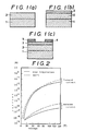
- FIG.1(a) is a sectional view of a p+-type diamond grown on a diamond monocrystalline substrate for showing the first step of producing an embodiment of this invention.
- FIG.1(b) is a sectional view of a non-doped diamond layer deposited on the p+-type diamond for showing the second step of producing the same embodiment.
- FIG.1(c) is a sectional view of electrodes coated on the non-doped diamond layer for showing the third step of producing the same embodiment.
- FIG.2 is a graph of the voltage - current relation of the Schottky diode shown by FIG.1(c) of the first embodiment of this invention.
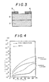
- FIG.3 is a sectional view of a Schottky diode as a comparison example.
- FIG.4 is a graph of the voltage - current relation of the Schottky diode of the comparison example.
- FIG.5 is a sectioned view of a semiconductor device as the third embodiment.
- FIG.6(a) is a sectional view of p+-type diamond grown on a diamond monocrystalline substrate for showing the first step of producing the third embodiment of the invention.
- FIG.6(b) is a sectional view of a non-doped diamond layer deposited on the p+-type diamond for showing the second step of producing the third embodiment.
- FIG.6(c) is a sectional view of electrodes deposited on the non-doped diamond layer for showing the third step of producing the third embodiment.
- a Schottky diode shown in FIG.1 is produced by the teaching of this invention. The processes of production are explained by referring to FIG.1(a), (b), and (c).
- the conditions of the microwave plasma CVD are as follows ;
- the concentration of boron in the p+-type diamond is 3 x 1020 cm ⁇ 3.
- p+ means " high doped p-type ".
- FIG.1(b) shows the substrate (1) coated with the p+-type layer (2) and the non-doped layer (3).
- FIG.1(c) shows the Schottky diode.
- the voltage - current relations are examined at room temperature and at 300°C.
- the titanium ohmic electrode (4) is connected to the ground level.
- Forward voltage or reverse voltage is applied on the aluminum Schottky electrode (5).
- the forward current which flows from the titanium electrode (4) to the aluminum electrode (5) is measured, while the forward voltage is applied between the electrodes (4) and (5).
- forward means the direction from the titanium electrode (4) to the aluminum electrode (5).
- the negative voltage applied to the aluminum electrode is called the forward voltage.
- FIG.2 shows the results of the measurements.
- the abscissa is the voltage ( V ) applied.
- the ordinate is the current ( A ).
- the reverse voltage and the reverse current are negative quantities, the relation therebetween is also depicted together with the forward current-voltage relation in FIG.2 for simplicity.
- the upper curves in FIG.2 show the forward voltage - current relation. Solid line denotes the relation at room temperature. Dotted line denotes the relation at 300°C. These curves show enough large forward currents. The forward currents increase according to rising of temperature. The two curves are not distanced so far in spite of the difference of temperature. This proves the high stability of the device against the change of temperature.
- the carrier concentration does not change so much by the change of temperature, because the high doped diamond has too many dopants ( more than 1018 cm ⁇ 3 ) and electronic states are already degenerated in the conduction band or the hole states are degenerated in the valence band.
- the thermal stability shows high carrier mobilities, because of the bigness of he forward currents. This is because the carriers flow in the non- or low doped diamond without being scattered by the heavily-doped dopants in the high doped diamond. Namely, these good features of the device derive from the fact that the carriers are supplied by the high doped diamond but they flow in the non- or low doped diamond. Then, the dynamics of transference of carriers is now briefly explained. If the carriers supplied by the high doped diamond layer were to stay in the high doped diamond layer, carriers would have been scattered frequently, and the forward current would be very low. In practice, the carriers are transferred from the high doped diamond to the non-doped diamond by diffusion or the electric field applied.
- the high doped diamond has plenty of carriers and the non-doped diamond has little carriers, the carriers will diffuse by the action of the inclination of the carrier concentration. If the interface between the high doped diamond layer and the non-doped diamond layer has been made in good order, the diffusion will occur furiously, because the difference of carrier concentrations is very large.
- the impurity concentration of the high doped diamond layer is 1018 cm ⁇ 3 to 1022 cm ⁇ 3.
- the impurity concentration of the non- or low doped diamond layer is less than 1017 cm ⁇ 3.
- the transference of carriers leaves the dopants being ionized.
- the ionized dopants positively charged donners or negatively charged acceptors ; cause Coulomb attraction for the transferred carriers. This Coulomb attraction pulls the carriers back to the high doped diamond layer.
- the balance of the diffusion and the Coulomb attraction determines the number of the carriers transferred into the non- or low doped diamond layer.
- Another force for transferring the carriers from the high doped layer to the non-doped layer is an electric field applied on the layers.
- the electric field When the electric field is applied in the direction vertical to the interface, the electric field carries the carriers by the electrostatic force into the non-doped diamond layer. Such vertical electric field will be explained later by the embodiment 2.
- the carriers borne in the high doped diamond ( p+-type ) layer (2) are transferred into the non-doped diamond layer (3). Since the non-doped diamond layer (3) has little impurities, the carriers can move freely without being scattered.
- the voltage applied between the electrodes (4) and (5) makes horizontal electric field in the non-doped layer (3) and in the p+-type ( high doped ) layer (2).
- the carriers in the non-doped layer (3) run with high speed because of the high carrier mobility. But the carriers left in the high doped layer (2) run with low speed, being scattered frequently by the dopants. Thus, the electric field does not penetrate into the high doped layer (2). Because the electric field is almost rejected from the high doped layer (2), the carriers there are moved only little. Thus, the energy loss induced by the carriers scattered by the dopants in the high doped layer (2) is trivial in spite of the low mobility of carriers.
- the lower curves show the reverse voltage - current relation.
- the reverse currents are small enough.
- the rectifying ratio quotient of the forward current to the reverse current at the same voltage; attains to 105.
- the breakdown voltage does not exist below 140 V.
- the embodiment 1 exhibits excellent performance as a Schottky diode.
- the comparison example has only a single p-type diamond layer (6) instead of the p-doped layer (2) and the non-doped layer (3) in the embodiment 1.
- the p-type diamond layer of the comparison example is 10.5 ⁇ m in thickness.
- the boron concentration is 1717 cm ⁇ 3.
- a titanium electrode (4) and an aluminum electrode (5) are formed on the p-type diamond layer (6).
- the titanium electrode (4) is an ohmic contact electrode and the aluminum electrode (5) is a Schottky contact electrode.
- the holes supplied by the dopant atoms in the p-type layer (6) run through the same p-type layer (6), being scattered by the dopant atoms.
- FIG.4 shown the relation of the voltage - current of the comparison example.
- the solid lines show the result of the measurement at room temperature.
- the dotted lines show the result at 300°C.
- both the forward current and the reverse current are small.
- the concentration of free holes is too small, because the dopant level is so deep that most of the carriers do not separate from the acceptors. Small number of free holes leads to the low forward current.
- the forward current at 300°C is about hundred times as much as the forward current at room temperature.
- the comparison example has a drawback that the breakdown voltage is as low as 80 V to 90 V.
- the thermal instability is caused from the low concentration of dopants ( 1017 cm ⁇ 3 ).
- the hole states are not degenerated at room temperature in the valence band, because of the low concentration of dopants and the deep dopant level.
- the highly-doped ( 3 X 1020 cm ⁇ 3 ) diamond layer (2) of the embodiment 1 has, even at room temperature, almost degenerated hole states in the valence band.
- the concentration of dopant in the p-type layer (6) was raised, the problem of the drastic change of carrier concentration as a function of temperature would be solved but the free holes would not run so fast by the scattering owing to the disorder of lattice that the forward current would be very small.
- the concentration of dopant should not be raised so much higher than 1017 cm ⁇ 3 in the p-type layer (6) of the comparison example.
- the low breakdown voltage 80 V to 90 V is perhaps caused partly by the disorder of lattice owing to the doping and partly by the thin depletion layer at the Schottky junction. Since the thickness of the depletion layer is inversely proportional to the root square of the dopant concentration, the depletion layer in the p-type layer (6) of the comparison example is much thinner than the depletion layer in the non-doped layer (3) of the embodiment 1.
- the results of FIG.2 and FIG.4 confirm the excellency of the embodiment 1 in the thermal stability and the high breakdown voltage.
- Embodiment 2 is a Schottky diode having a low doped diamond layer instead of the non-doped diamond layer (3) of the embodiment 1.
- the low doped layer is a p-type layer doped with boron of 1016 cm ⁇ 3 in concentration.
- Other structures are all the same as the embodiment 1 except for the replacement of the non-doped diamond layer (3) by the low doped diamond layer.
- the forward currents and reverse currents are measured by applying the forward voltage or reverse voltage.
- the rectifying ratio is about 104.
- the forward current at 300°C is nearly twice as much as the forward current at room temperature.
- the change of the forward current owing to the change of temperature is much less than the change of the comparison example shown by FIG. 4.
- the Schottky diode shown in FIG.5 is fabricated by the teaching of this invention.
- the Schottky diode comprises a p-type Si substrate (7), a p+-type diamond layer (8), a non-doped diamond layer (9), a tungsten ( W ) electrode (10) and a gold ( Au ) electrode (11).
- a FET ( Field Effect Transistor) shown in FIG.6 is fabricated by the teaching of this invention.
Landscapes
- Electrodes Of Semiconductors (AREA)
- Junction Field-Effect Transistors (AREA)
- Bipolar Transistors (AREA)
Applications Claiming Priority (2)
| Application Number | Priority Date | Filing Date | Title |
|---|---|---|---|
| JP2128563A JP2961812B2 (ja) | 1990-05-17 | 1990-05-17 | 半導体装置 |
| JP128563/90 | 1990-05-17 |
Publications (3)
| Publication Number | Publication Date |
|---|---|
| EP0457508A2 true EP0457508A2 (fr) | 1991-11-21 |
| EP0457508A3 EP0457508A3 (en) | 1992-03-25 |
| EP0457508B1 EP0457508B1 (fr) | 1997-08-20 |
Family
ID=14987859
Family Applications (1)
| Application Number | Title | Priority Date | Filing Date |
|---|---|---|---|
| EP91304212A Expired - Lifetime EP0457508B1 (fr) | 1990-05-17 | 1991-05-10 | Dispositif semi-conducteur en diamant |
Country Status (4)
| Country | Link |
|---|---|
| US (1) | US5252840A (fr) |
| EP (1) | EP0457508B1 (fr) |
| JP (1) | JP2961812B2 (fr) |
| DE (1) | DE69127314T2 (fr) |
Cited By (20)
| Publication number | Priority date | Publication date | Assignee | Title |
|---|---|---|---|---|
| US5285084A (en) * | 1992-09-02 | 1994-02-08 | Kobe Steel Usa | Diamond schottky diodes and gas sensors fabricated therefrom |
| US5362975A (en) * | 1992-09-02 | 1994-11-08 | Kobe Steel Usa | Diamond-based chemical sensors |
| GB2254732B (en) * | 1991-03-29 | 1994-11-30 | Kobe Steel Ltd | Diamond schottky diode |
| EP0643423A3 (fr) * | 1993-09-10 | 1995-08-09 | Sumitomo Electric Industries | Dispositif semi-conducteur en diamant. |
| DE4415600A1 (de) * | 1994-05-04 | 1995-11-30 | Daimler Benz Ag | Elektronisches Bauteil mit einer Halbleiter-Komposit-Struktur |
| EP0681314A3 (fr) * | 1994-05-04 | 1996-09-04 | Daimler Benz Ag | Structure composite pour dispositif électronique et procédé de fabrication. |
| EP0646970A3 (fr) * | 1993-09-24 | 1996-11-06 | Sumitomo Electric Industries | Dispositif à semi-conducteur ayant des niveaux d'impureté profonds pour opération à haute température. |
| EP0702413A3 (fr) * | 1994-09-16 | 1996-11-13 | Sumitomo Electric Industries | Transistor à effet de champ MES formé dans une couche de diamant |
| US5843224A (en) * | 1994-08-05 | 1998-12-01 | Daimler-Benz Aktiengesellschaft | Composite structure comprising a semiconductor layer arranged on a diamond or diamond-like layer and process for its production |
| DE19738512A1 (de) * | 1997-09-03 | 1999-02-18 | Daimler Benz Ag | Diamantschicht eines mikroelektronischen Bauteils und Verfahren zu deren Herstellung |
| DE19514546C2 (de) * | 1995-04-20 | 2000-11-09 | Daimler Chrysler Ag | Elektronisches Bauteil mit einer Komposit-Struktur |
| DE102004006544B3 (de) * | 2004-02-10 | 2005-09-08 | Infineon Technologies Ag | Verfahren zur Abscheidung eines leitfähigen Kohlenstoffmaterials auf einem Halbleiter zur Ausbildung eines Schottky-Kontaktes und Halbleiterkontaktvorrichtung |
| WO2006013430A1 (fr) * | 2004-07-27 | 2006-02-09 | Element Six Limited | Électrodes en diamant |
| WO2010075124A1 (fr) * | 2008-12-22 | 2010-07-01 | Raytheon Company | Fabrication d'une couche de nitrure de gallium avec des couches de diamant |
| WO2010075125A1 (fr) * | 2008-12-22 | 2010-07-01 | Raytheon Company | Fabrication d'un dispositif au nitrure de gallium avec une couche de diamant |
| US7768016B2 (en) | 2008-02-11 | 2010-08-03 | Qimonda Ag | Carbon diode array for resistivity changing memories |
| US7892881B2 (en) | 2009-02-23 | 2011-02-22 | Raytheon Company | Fabricating a device with a diamond layer |
| US7894253B2 (en) | 2006-10-27 | 2011-02-22 | Qimonda Ag | Carbon filament memory and fabrication method |
| US7915603B2 (en) | 2006-10-27 | 2011-03-29 | Qimonda Ag | Modifiable gate stack memory element |
| US8030637B2 (en) | 2006-08-25 | 2011-10-04 | Qimonda Ag | Memory element using reversible switching between SP2 and SP3 hybridized carbon |
Families Citing this family (21)
| Publication number | Priority date | Publication date | Assignee | Title |
|---|---|---|---|---|
| US5371382A (en) * | 1992-04-27 | 1994-12-06 | Kobe Steel Usa, Inc. | Amorphous silicon rectifying contact on diamond and method for making same |
| US5382812A (en) * | 1993-04-14 | 1995-01-17 | Kobe Development Corporation | Diamond and II-VI heterojunction semiconductor light emitting device |
| DE4322650A1 (de) * | 1993-07-07 | 1995-01-12 | Siemens Ag | Temperatursensor mit einem p-n-Übergang |
| JPH07161455A (ja) * | 1993-12-09 | 1995-06-23 | Sumitomo Electric Ind Ltd | ダイヤモンドヒ−タ |
| US5536953A (en) * | 1994-03-08 | 1996-07-16 | Kobe Steel Usa | Wide bandgap semiconductor device including lightly doped active region |
| JPH07283434A (ja) * | 1994-04-07 | 1995-10-27 | Kobe Steel Ltd | ダイヤモンド発光素子 |
| EP0697726B1 (fr) * | 1994-08-03 | 2003-02-26 | Sumitomo Electric Industries, Ltd. | Dissipateur de chaleur fabriqué d'une couche en diamant synthétique |
| US5592053A (en) * | 1994-12-06 | 1997-01-07 | Kobe Steel Usa, Inc. | Diamond target electron beam device |
| US6582513B1 (en) * | 1998-05-15 | 2003-06-24 | Apollo Diamond, Inc. | System and method for producing synthetic diamond |
| US6858080B2 (en) * | 1998-05-15 | 2005-02-22 | Apollo Diamond, Inc. | Tunable CVD diamond structures |
| EP1693895B1 (fr) * | 2003-11-25 | 2013-03-13 | Sumitomo Electric Industries, Ltd. | Semi-conducteur de diamant de type n, procede de fabrication, element semi-conducteur, et element emetteur d'electrons |
| WO2005080645A2 (fr) * | 2004-02-13 | 2005-09-01 | Apollo Diamond, Inc. | Separation de structure de diamant |
| KR100636349B1 (ko) * | 2004-09-24 | 2006-10-19 | 엘지전자 주식회사 | 마이크로렌즈 배열 시트 및 그 제작방법 |
| US20060163584A1 (en) * | 2005-01-26 | 2006-07-27 | Robert Linares | Boron-doped diamond semiconductor |
| DE102005028216A1 (de) | 2005-06-17 | 2006-12-28 | Siemens Ag | Vorrichtung und Verfahren für die Computertomographie |
| JP4858948B2 (ja) * | 2006-01-17 | 2012-01-18 | 独立行政法人産業技術総合研究所 | 不純物傾斜型ダイヤモンド薄膜及びその製造方法並びに該不純物傾斜型ダイヤモンド薄膜を用いたダイオード又はトランジスタ |
| US20090050899A1 (en) * | 2007-08-23 | 2009-02-26 | National Institute of Advanced Industrial Scinece and Technology | High-output diamond semiconductor element |
| JP2009059798A (ja) * | 2007-08-30 | 2009-03-19 | Sumitomo Electric Ind Ltd | ダイヤモンド電子素子の製造方法 |
| JP2009200343A (ja) * | 2008-02-22 | 2009-09-03 | Sumitomo Electric Ind Ltd | ダイヤモンド電子素子 |
| JP6444718B2 (ja) * | 2014-12-15 | 2018-12-26 | 株式会社東芝 | 半導体装置 |
| DE102021123907A1 (de) | 2021-09-15 | 2023-03-16 | Universität Siegen, Körperschaft des öffentlichen Rechts | LED und Herstellungsverfahren dafür |
Family Cites Families (10)
| Publication number | Priority date | Publication date | Assignee | Title |
|---|---|---|---|---|
| JPS57121288A (en) * | 1981-01-20 | 1982-07-28 | Sanyo Electric Co Ltd | Hall element |
| JPS58141572A (ja) * | 1982-02-18 | 1983-08-22 | Seiko Epson Corp | 半導体装置 |
| JPS59208821A (ja) * | 1983-05-13 | 1984-11-27 | Sumitomo Electric Ind Ltd | 気相合成によるダイヤモンド半導体およびその製造方法 |
| JPS59213126A (ja) * | 1983-05-19 | 1984-12-03 | Sumitomo Electric Ind Ltd | ダイヤモンド半導体素子の製造法 |
| JP2614868B2 (ja) * | 1987-09-09 | 1997-05-28 | 導電性無機化合物技術研究組合 | 電界効果トランジスタの製造法 |
| US4929986A (en) * | 1987-09-25 | 1990-05-29 | The United States Of America As Represented By The Secretary Of The Navy | High power diamond traveling wave amplifier |
| US5006914A (en) * | 1988-12-02 | 1991-04-09 | Advanced Technology Materials, Inc. | Single crystal semiconductor substrate articles and semiconductor devices comprising same |
| JPH02260470A (ja) * | 1989-03-30 | 1990-10-23 | Sumitomo Electric Ind Ltd | 発光素子 |
| JP2730271B2 (ja) * | 1990-03-07 | 1998-03-25 | 住友電気工業株式会社 | 半導体装置 |
| JP2813023B2 (ja) * | 1990-03-13 | 1998-10-22 | 株式会社神戸製鋼所 | Mis型ダイヤモンド電界効果トランジスタ |
-
1990
- 1990-05-17 JP JP2128563A patent/JP2961812B2/ja not_active Expired - Lifetime
-
1991
- 1991-05-09 US US07/697,438 patent/US5252840A/en not_active Expired - Lifetime
- 1991-05-10 EP EP91304212A patent/EP0457508B1/fr not_active Expired - Lifetime
- 1991-05-10 DE DE69127314T patent/DE69127314T2/de not_active Expired - Fee Related
Cited By (31)
| Publication number | Priority date | Publication date | Assignee | Title |
|---|---|---|---|---|
| GB2254732B (en) * | 1991-03-29 | 1994-11-30 | Kobe Steel Ltd | Diamond schottky diode |
| US5362975A (en) * | 1992-09-02 | 1994-11-08 | Kobe Steel Usa | Diamond-based chemical sensors |
| US5285084A (en) * | 1992-09-02 | 1994-02-08 | Kobe Steel Usa | Diamond schottky diodes and gas sensors fabricated therefrom |
| US5600156A (en) * | 1993-09-10 | 1997-02-04 | Sumitomo Electric Industries, Ltd. | Diamond semiconductor device with P-I-N type multilayer structure |
| EP0643423A3 (fr) * | 1993-09-10 | 1995-08-09 | Sumitomo Electric Industries | Dispositif semi-conducteur en diamant. |
| EP0646970A3 (fr) * | 1993-09-24 | 1996-11-06 | Sumitomo Electric Industries | Dispositif à semi-conducteur ayant des niveaux d'impureté profonds pour opération à haute température. |
| US5670796A (en) * | 1993-09-24 | 1997-09-23 | Sumitomo Electric Industries, Ltd. | Semiconductor device consisting of a semiconductor material having a deep impurity level |
| EP0681314A3 (fr) * | 1994-05-04 | 1996-09-04 | Daimler Benz Ag | Structure composite pour dispositif électronique et procédé de fabrication. |
| US5744825A (en) * | 1994-05-04 | 1998-04-28 | Daimler-Benz Ag | Composite structure for an electronic component comprising a growth substrate, a diamond layer, and an intermediate layer therebetween |
| DE4415600A1 (de) * | 1994-05-04 | 1995-11-30 | Daimler Benz Ag | Elektronisches Bauteil mit einer Halbleiter-Komposit-Struktur |
| US5843224A (en) * | 1994-08-05 | 1998-12-01 | Daimler-Benz Aktiengesellschaft | Composite structure comprising a semiconductor layer arranged on a diamond or diamond-like layer and process for its production |
| US5903015A (en) * | 1994-09-16 | 1999-05-11 | Sumitomo Electric Industries, Ltd. | Field effect transistor using diamond |
| EP0702413A3 (fr) * | 1994-09-16 | 1996-11-13 | Sumitomo Electric Industries | Transistor à effet de champ MES formé dans une couche de diamant |
| DE19514546C2 (de) * | 1995-04-20 | 2000-11-09 | Daimler Chrysler Ag | Elektronisches Bauteil mit einer Komposit-Struktur |
| DE19738512A1 (de) * | 1997-09-03 | 1999-02-18 | Daimler Benz Ag | Diamantschicht eines mikroelektronischen Bauteils und Verfahren zu deren Herstellung |
| DE102004006544B3 (de) * | 2004-02-10 | 2005-09-08 | Infineon Technologies Ag | Verfahren zur Abscheidung eines leitfähigen Kohlenstoffmaterials auf einem Halbleiter zur Ausbildung eines Schottky-Kontaktes und Halbleiterkontaktvorrichtung |
| WO2006013430A1 (fr) * | 2004-07-27 | 2006-02-09 | Element Six Limited | Électrodes en diamant |
| US8030637B2 (en) | 2006-08-25 | 2011-10-04 | Qimonda Ag | Memory element using reversible switching between SP2 and SP3 hybridized carbon |
| US7894253B2 (en) | 2006-10-27 | 2011-02-22 | Qimonda Ag | Carbon filament memory and fabrication method |
| US7915603B2 (en) | 2006-10-27 | 2011-03-29 | Qimonda Ag | Modifiable gate stack memory element |
| US7768016B2 (en) | 2008-02-11 | 2010-08-03 | Qimonda Ag | Carbon diode array for resistivity changing memories |
| WO2010075125A1 (fr) * | 2008-12-22 | 2010-07-01 | Raytheon Company | Fabrication d'un dispositif au nitrure de gallium avec une couche de diamant |
| US7888171B2 (en) | 2008-12-22 | 2011-02-15 | Raytheon Company | Fabricating a gallium nitride layer with diamond layers |
| US7884373B2 (en) | 2008-12-22 | 2011-02-08 | Raytheon Company | Gallium nitride layer with diamond layers |
| US7989261B2 (en) | 2008-12-22 | 2011-08-02 | Raytheon Company | Fabricating a gallium nitride device with a diamond layer |
| WO2010075124A1 (fr) * | 2008-12-22 | 2010-07-01 | Raytheon Company | Fabrication d'une couche de nitrure de gallium avec des couches de diamant |
| US8174024B2 (en) | 2008-12-22 | 2012-05-08 | Raytheon Company | Gallium nitride device with a diamond layer |
| KR101227925B1 (ko) | 2008-12-22 | 2013-01-30 | 레이티언 캄파니 | 다이아몬드 층을 갖는 갈륨 질화물 장치 제조 |
| KR101227923B1 (ko) | 2008-12-22 | 2013-01-30 | 레이티언 캄파니 | 다이아몬드 층을 갖는 갈륨 질화물 층 제조 |
| TWI461563B (zh) * | 2008-12-22 | 2014-11-21 | 雷森公司 | 製造具有鑽石層之氮化鎵層 |
| US7892881B2 (en) | 2009-02-23 | 2011-02-22 | Raytheon Company | Fabricating a device with a diamond layer |
Also Published As
| Publication number | Publication date |
|---|---|
| DE69127314T2 (de) | 1997-12-18 |
| DE69127314D1 (de) | 1997-09-25 |
| JP2961812B2 (ja) | 1999-10-12 |
| EP0457508B1 (fr) | 1997-08-20 |
| EP0457508A3 (en) | 1992-03-25 |
| JPH0422172A (ja) | 1992-01-27 |
| US5252840A (en) | 1993-10-12 |
Similar Documents
| Publication | Publication Date | Title |
|---|---|---|
| EP0457508B1 (fr) | Dispositif semi-conducteur en diamant | |
| US5132749A (en) | Semiconductor device | |
| Jian et al. | Temperature-dependent current-voltage characteristics of β-Ga2O3 trench Schottky barrier diodes | |
| Hu et al. | Near unity ideality factor and Shockley-Read-Hall lifetime in GaN-on-GaN pn diodes with avalanche breakdown | |
| Rideout | A review of the theory and technology for ohmic contacts to group III–V compound semiconductors | |
| US6218677B1 (en) | III-V nitride resonant tunneling | |
| US4173763A (en) | Heterojunction tunneling base transistor | |
| JP2671259B2 (ja) | ショットキー接合半導体装置 | |
| JP5054255B2 (ja) | シリコン・カーバイド・パワー・トランジスタの最大電圧を増大させるための構造 | |
| JPH0652812B2 (ja) | 金属−絶縁体−金属接合構造の製造方法 | |
| EP0643423B1 (fr) | Dispositif semi-conducteur en diamant | |
| Aleksov et al. | Diamond diodes and transistors | |
| US6287946B1 (en) | Fabrication of low resistance, non-alloyed, ohmic contacts to InP using non-stoichiometric InP layers | |
| Pankove et al. | High-temperature GaN/SiC heterojunction bipolar transistor with high gain | |
| JP3058345B2 (ja) | 半導体素子 | |
| US5371378A (en) | Diamond metal base/permeable base transistor and method of making same | |
| EP0646970B1 (fr) | Dispositif à semi-conducteur ayant des niveaux d'impureté profonds pour opération à haute température | |
| US4590502A (en) | Camel gate field effect transistor device | |
| US5298766A (en) | Diamond heterojunction diode | |
| Bandić et al. | Nitride based high power devices: design and fabrication issues | |
| Cho et al. | Properties of Schottky barriers and p‐n junctions prepared with GaAs and Al x Ga1− x As molecular beam epitaxial layers | |
| Hirose et al. | New SiGe bipolar transistors and pin diodes for power switching | |
| US4569118A (en) | Planar gate turn-off field controlled thyristors and planar junction gate field effect transistors, and method of making same | |
| KR100944883B1 (ko) | Pn 접합을 갖는 박막 결정 웨이퍼 및 그 제조 공정 | |
| US5982024A (en) | High concentration doped semiconductor |
Legal Events
| Date | Code | Title | Description |
|---|---|---|---|
| PUAI | Public reference made under article 153(3) epc to a published international application that has entered the european phase |
Free format text: ORIGINAL CODE: 0009012 |
|
| AK | Designated contracting states |
Kind code of ref document: A2 Designated state(s): DE FR GB NL |
|
| PUAL | Search report despatched |
Free format text: ORIGINAL CODE: 0009013 |
|
| AK | Designated contracting states |
Kind code of ref document: A3 Designated state(s): DE FR GB NL |
|
| 17P | Request for examination filed |
Effective date: 19920902 |
|
| 17Q | First examination report despatched |
Effective date: 19941118 |
|
| GRAG | Despatch of communication of intention to grant |
Free format text: ORIGINAL CODE: EPIDOS AGRA |
|
| GRAH | Despatch of communication of intention to grant a patent |
Free format text: ORIGINAL CODE: EPIDOS IGRA |
|
| GRAH | Despatch of communication of intention to grant a patent |
Free format text: ORIGINAL CODE: EPIDOS IGRA |
|
| GRAA | (expected) grant |
Free format text: ORIGINAL CODE: 0009210 |
|
| AK | Designated contracting states |
Kind code of ref document: B1 Designated state(s): DE FR GB NL |
|
| REF | Corresponds to: |
Ref document number: 69127314 Country of ref document: DE Date of ref document: 19970925 |
|
| ET | Fr: translation filed | ||
| RAP2 | Party data changed (patent owner data changed or rights of a patent transferred) |
Owner name: SUMITOMO ELECTRIC INDUSTRIES, LTD. |
|
| NLT2 | Nl: modifications (of names), taken from the european patent patent bulletin |
Owner name: SUMITOMO ELECTRIC INDUSTRIES, LTD. |
|
| NLXE | Nl: other communications concerning ep-patents (part 3 heading xe) |
Free format text: PAT. BUL. 01/98 PAGE 41: SHOULD BE MODIFIED INTO: SUMITOMO ELECTRIC INDUSTRIES, LTD. |
|
| PLBE | No opposition filed within time limit |
Free format text: ORIGINAL CODE: 0009261 |
|
| STAA | Information on the status of an ep patent application or granted ep patent |
Free format text: STATUS: NO OPPOSITION FILED WITHIN TIME LIMIT |
|
| 26N | No opposition filed | ||
| REG | Reference to a national code |
Ref country code: GB Ref legal event code: IF02 |
|
| PGFP | Annual fee paid to national office [announced via postgrant information from national office to epo] |
Ref country code: NL Payment date: 20080501 Year of fee payment: 18 |
|
| PGFP | Annual fee paid to national office [announced via postgrant information from national office to epo] |
Ref country code: DE Payment date: 20090511 Year of fee payment: 19 |
|
| PGFP | Annual fee paid to national office [announced via postgrant information from national office to epo] |
Ref country code: GB Payment date: 20090506 Year of fee payment: 19 |
|
| NLV4 | Nl: lapsed or anulled due to non-payment of the annual fee |
Effective date: 20091201 |
|
| PG25 | Lapsed in a contracting state [announced via postgrant information from national office to epo] |
Ref country code: NL Free format text: LAPSE BECAUSE OF NON-PAYMENT OF DUE FEES Effective date: 20091201 |
|
| REG | Reference to a national code |
Ref country code: FR Ref legal event code: ST Effective date: 20100129 |
|
| PG25 | Lapsed in a contracting state [announced via postgrant information from national office to epo] |
Ref country code: FR Free format text: LAPSE BECAUSE OF NON-PAYMENT OF DUE FEES Effective date: 20090602 |
|
| PGFP | Annual fee paid to national office [announced via postgrant information from national office to epo] |
Ref country code: FR Payment date: 20080514 Year of fee payment: 18 |
|
| GBPC | Gb: european patent ceased through non-payment of renewal fee |
Effective date: 20100510 |
|
| PG25 | Lapsed in a contracting state [announced via postgrant information from national office to epo] |
Ref country code: DE Free format text: LAPSE BECAUSE OF NON-PAYMENT OF DUE FEES Effective date: 20101201 |
|
| PG25 | Lapsed in a contracting state [announced via postgrant information from national office to epo] |
Ref country code: GB Free format text: LAPSE BECAUSE OF NON-PAYMENT OF DUE FEES Effective date: 20100510 |