EP0457670A1 - Verfahren zur Herstellung eines Anzeigeschirmes mit aktiver Matrix und Speicherkondensatoren sowie der durch dieses Verfahren hergestellte Schirm - Google Patents
Verfahren zur Herstellung eines Anzeigeschirmes mit aktiver Matrix und Speicherkondensatoren sowie der durch dieses Verfahren hergestellte Schirm Download PDFInfo
- Publication number
- EP0457670A1 EP0457670A1 EP91401241A EP91401241A EP0457670A1 EP 0457670 A1 EP0457670 A1 EP 0457670A1 EP 91401241 A EP91401241 A EP 91401241A EP 91401241 A EP91401241 A EP 91401241A EP 0457670 A1 EP0457670 A1 EP 0457670A1
- Authority
- EP
- European Patent Office
- Prior art keywords
- lines
- addressing
- column
- block
- appendices
- Prior art date
- Legal status (The legal status is an assumption and is not a legal conclusion. Google has not performed a legal analysis and makes no representation as to the accuracy of the status listed.)
- Granted
Links
- 239000003990 capacitor Substances 0.000 title claims abstract description 36
- 238000003860 storage Methods 0.000 title claims abstract description 35
- 238000000034 method Methods 0.000 title claims abstract description 23
- 239000011159 matrix material Substances 0.000 title claims abstract description 10
- 238000004519 manufacturing process Methods 0.000 title claims abstract description 5
- 230000000873 masking effect Effects 0.000 claims abstract description 11
- 238000005530 etching Methods 0.000 claims description 15
- 239000004065 semiconductor Substances 0.000 claims description 8
- 239000004020 conductor Substances 0.000 claims description 6
- 239000000758 substrate Substances 0.000 claims description 4
- 239000012212 insulator Substances 0.000 claims description 3
- 239000000463 material Substances 0.000 claims 2
- 238000009432 framing Methods 0.000 claims 1
- 239000004973 liquid crystal related substance Substances 0.000 abstract description 6
- 239000011521 glass Substances 0.000 description 3
- 229910021417 amorphous silicon Inorganic materials 0.000 description 2
- 230000008021 deposition Effects 0.000 description 2
- 238000010586 diagram Methods 0.000 description 2
- 230000000694 effects Effects 0.000 description 2
- 229910052751 metal Inorganic materials 0.000 description 2
- 239000002184 metal Substances 0.000 description 2
- 239000010409 thin film Substances 0.000 description 2
- 229910052581 Si3N4 Inorganic materials 0.000 description 1
- ATJFFYVFTNAWJD-UHFFFAOYSA-N Tin Chemical compound [Sn] ATJFFYVFTNAWJD-UHFFFAOYSA-N 0.000 description 1
- 241001639412 Verres Species 0.000 description 1
- 229910052782 aluminium Inorganic materials 0.000 description 1
- XAGFODPZIPBFFR-UHFFFAOYSA-N aluminium Chemical compound [Al] XAGFODPZIPBFFR-UHFFFAOYSA-N 0.000 description 1
- 238000004140 cleaning Methods 0.000 description 1
- 230000007423 decrease Effects 0.000 description 1
- 229910052738 indium Inorganic materials 0.000 description 1
- APFVFJFRJDLVQX-UHFFFAOYSA-N indium atom Chemical compound [In] APFVFJFRJDLVQX-UHFFFAOYSA-N 0.000 description 1
- 229910003437 indium oxide Inorganic materials 0.000 description 1
- PJXISJQVUVHSOJ-UHFFFAOYSA-N indium(iii) oxide Chemical compound [O-2].[O-2].[O-2].[In+3].[In+3] PJXISJQVUVHSOJ-UHFFFAOYSA-N 0.000 description 1
- AMGQUBHHOARCQH-UHFFFAOYSA-N indium;oxotin Chemical compound [In].[Sn]=O AMGQUBHHOARCQH-UHFFFAOYSA-N 0.000 description 1
- 238000000206 photolithography Methods 0.000 description 1
- 238000002360 preparation method Methods 0.000 description 1
- 230000002787 reinforcement Effects 0.000 description 1
- 238000000926 separation method Methods 0.000 description 1
- 229910052710 silicon Inorganic materials 0.000 description 1
- 239000010703 silicon Substances 0.000 description 1
- HQVNEWCFYHHQES-UHFFFAOYSA-N silicon nitride Chemical compound N12[Si]34N5[Si]62N3[Si]51N64 HQVNEWCFYHHQES-UHFFFAOYSA-N 0.000 description 1
- 239000000126 substance Substances 0.000 description 1
- 229910001887 tin oxide Inorganic materials 0.000 description 1
Images


Classifications
-
- G—PHYSICS
- G02—OPTICS
- G02F—OPTICAL DEVICES OR ARRANGEMENTS FOR THE CONTROL OF LIGHT BY MODIFICATION OF THE OPTICAL PROPERTIES OF THE MEDIA OF THE ELEMENTS INVOLVED THEREIN; NON-LINEAR OPTICS; FREQUENCY-CHANGING OF LIGHT; OPTICAL LOGIC ELEMENTS; OPTICAL ANALOGUE/DIGITAL CONVERTERS
- G02F1/00—Devices or arrangements for the control of the intensity, colour, phase, polarisation or direction of light arriving from an independent light source, e.g. switching, gating or modulating; Non-linear optics
- G02F1/01—Devices or arrangements for the control of the intensity, colour, phase, polarisation or direction of light arriving from an independent light source, e.g. switching, gating or modulating; Non-linear optics for the control of the intensity, phase, polarisation or colour
- G02F1/13—Devices or arrangements for the control of the intensity, colour, phase, polarisation or direction of light arriving from an independent light source, e.g. switching, gating or modulating; Non-linear optics for the control of the intensity, phase, polarisation or colour based on liquid crystals, e.g. single liquid crystal display cells
- G02F1/133—Constructional arrangements; Operation of liquid crystal cells; Circuit arrangements
- G02F1/136—Liquid crystal cells structurally associated with a semi-conducting layer or substrate, e.g. cells forming part of an integrated circuit
- G02F1/1362—Active matrix addressed cells
- G02F1/136213—Storage capacitors associated with the pixel electrode
-
- G—PHYSICS
- G02—OPTICS
- G02F—OPTICAL DEVICES OR ARRANGEMENTS FOR THE CONTROL OF LIGHT BY MODIFICATION OF THE OPTICAL PROPERTIES OF THE MEDIA OF THE ELEMENTS INVOLVED THEREIN; NON-LINEAR OPTICS; FREQUENCY-CHANGING OF LIGHT; OPTICAL LOGIC ELEMENTS; OPTICAL ANALOGUE/DIGITAL CONVERTERS
- G02F1/00—Devices or arrangements for the control of the intensity, colour, phase, polarisation or direction of light arriving from an independent light source, e.g. switching, gating or modulating; Non-linear optics
- G02F1/01—Devices or arrangements for the control of the intensity, colour, phase, polarisation or direction of light arriving from an independent light source, e.g. switching, gating or modulating; Non-linear optics for the control of the intensity, phase, polarisation or colour
- G02F1/13—Devices or arrangements for the control of the intensity, colour, phase, polarisation or direction of light arriving from an independent light source, e.g. switching, gating or modulating; Non-linear optics for the control of the intensity, phase, polarisation or colour based on liquid crystals, e.g. single liquid crystal display cells
- G02F1/133—Constructional arrangements; Operation of liquid crystal cells; Circuit arrangements
- G02F1/136—Liquid crystal cells structurally associated with a semi-conducting layer or substrate, e.g. cells forming part of an integrated circuit
- G02F1/1362—Active matrix addressed cells
- G02F1/13624—Active matrix addressed cells having more than one switching element per pixel
-
- G—PHYSICS
- G02—OPTICS
- G02F—OPTICAL DEVICES OR ARRANGEMENTS FOR THE CONTROL OF LIGHT BY MODIFICATION OF THE OPTICAL PROPERTIES OF THE MEDIA OF THE ELEMENTS INVOLVED THEREIN; NON-LINEAR OPTICS; FREQUENCY-CHANGING OF LIGHT; OPTICAL LOGIC ELEMENTS; OPTICAL ANALOGUE/DIGITAL CONVERTERS
- G02F1/00—Devices or arrangements for the control of the intensity, colour, phase, polarisation or direction of light arriving from an independent light source, e.g. switching, gating or modulating; Non-linear optics
- G02F1/01—Devices or arrangements for the control of the intensity, colour, phase, polarisation or direction of light arriving from an independent light source, e.g. switching, gating or modulating; Non-linear optics for the control of the intensity, phase, polarisation or colour
- G02F1/13—Devices or arrangements for the control of the intensity, colour, phase, polarisation or direction of light arriving from an independent light source, e.g. switching, gating or modulating; Non-linear optics for the control of the intensity, phase, polarisation or colour based on liquid crystals, e.g. single liquid crystal display cells
- G02F1/133—Constructional arrangements; Operation of liquid crystal cells; Circuit arrangements
- G02F1/136—Liquid crystal cells structurally associated with a semi-conducting layer or substrate, e.g. cells forming part of an integrated circuit
- G02F1/1362—Active matrix addressed cells
- G02F1/136259—Repairing; Defects
-
- Y—GENERAL TAGGING OF NEW TECHNOLOGICAL DEVELOPMENTS; GENERAL TAGGING OF CROSS-SECTIONAL TECHNOLOGIES SPANNING OVER SEVERAL SECTIONS OF THE IPC; TECHNICAL SUBJECTS COVERED BY FORMER USPC CROSS-REFERENCE ART COLLECTIONS [XRACs] AND DIGESTS
- Y10—TECHNICAL SUBJECTS COVERED BY FORMER USPC
- Y10S—TECHNICAL SUBJECTS COVERED BY FORMER USPC CROSS-REFERENCE ART COLLECTIONS [XRACs] AND DIGESTS
- Y10S148/00—Metal treatment
- Y10S148/014—Capacitor
Definitions
- the present invention relates to a method of producing an active matrix display screen and storage capacitors and a screen obtained by this method.
- an active matrix display screen consists schematically of two plates, the first being covered with a matrix of conducting blocks defining pixels, each block being associated with an addressing transistor itself controlled by addressing lines and columns and the second being covered with a counter electrode. A liquid crystal is inserted between the two plates.
- active matrix display screens have appeared, further comprising storage capacitors.
- the advantage of these capacitors is to limit the effects of the rise in temperature, which, in a traditional screen, decreases the time constant of the pixel capacity, the liquid crystal and the control transistor becoming the seat of currents leak.
- Display screens with active matrix and storage capacitors are described for example in document GB-A-2 115 199, in the article by D. TOMITA et al. entitled “A 6.5-in Diagonal TFT-LCD Module for Liquid Crystal TV” published in the journal SID 89 DIGEST, pp. 151-154 as well as in the article by Y. ASAI entitled “A 6.7-in Square High-Resolution Full-Color TFL-LCD” published in the magazine Japan Display 89, pp. 514-517.
- FIG. 1a shows a cell comprising a TFT transistor (this designation reminding us that it is generally a thin film transistor), a capacitor Clc corresponding to the liquid crystal inserted between the armature of the first plate and the counter-electrode brought to a potential VCE.
- the address line controlling the TFT grid is referenced L and the address column C.
- the cell of FIG. 1b differs from that of FIG. 1a by the presence of a storage capacitor Cs, one armature of which is connected to the TFT and the other is brought to a reference potential VR.
- Figures 2a and 2b show two ways to control a storage capacitor screen.
- the storage capacitors corresponding to the same line Ln have one of their armatures connected to a dedicated electrode LC, specially produced for this purpose, all the lines LC being joined to a reference strip LR arranged on the side of the screen and brought to a potential VR.
- the storage capacitors Cs specific to a line Ln + 1 have an armature connected to the previous line Ln.
- the reference potential VR can be the potential of the counter-electrode.
- the reference potential is that of the previous line. This potential is very fixed and can therefore serve as a reference during the frame time, except during the addressing time when its value is disturbed. This disturbance occurring just before the refresh of the line considered, it has no effect on the final potential of the pixel.
- the object of the present invention is to reduce this complexity and it aims more particularly to rediscover the simplicity of the process known as having two masking levels.
- the method is characterized in that the capacitive lines are lines dedicated to this function and are all connected to a strip located on the side of the screen.
- the method is characterized in that, during the second etching, the capacitive lines are merged with the address lines and overlap, on the one hand, with segments extending the blocks to form the storage capacitors and, on the other hand, the various column or block appendices to form the addressing transistors.
- the present application also relates to a display screen obtained by the process which has just been defined.
- This screen is of the type described in FR-A-2 533 072 and it is characterized in that it also comprises capacitive lines formed by said stack of layers, these lines overlapping part of the blocks, these lines forming storage capacitors connected to the pavers.
- the capacitive lines are lines specially added for the purpose of producing additional capacity.
- the capacitive lines are merged with the address lines and overlap, on the one hand, segments of blocks to form the storage capacitors and on the other hand, the various column and block appendices to form the addressing transistors.
- FIGS. 3, 4a and 4b show a display screen obtained according to an embodiment of the method of the invention.
- a layer of transparent conductive material 12 such as indium tin oxide ITO, is deposited.
- ITO indium tin oxide
- a first photogravure through a first masking level one obtains patterns made up of columns Cn, Cn + 1, etc ... and blocks P. These patterns correspond to the unshaded areas of the figure 3.
- Each block P is extended by an appendix, called appendix block AP.
- each column is extended by an appendage called appendix column AC, of curved shape.
- the paved appendage AP fits between the column and the curved appendage column AC. This arrangement is intended to obtain a double control transistor. But it is not compulsory.
- patterns such as the hatched patterns in FIG. 3 are defined, namely address lines Ln, Ln + 1, etc., capacitive lines LC and a reference band Br on the side of the screen.
- the addressing lines Ln, Ln + 1 define TFTs (double in the illustrated variant) and the lines LC define, with the conducting layer of block P which they cover, the desired storage capacitors Cs.
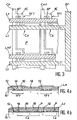
- Figure 4a corresponds to a section along an addressing line such as Ln and shows the double addressing transistors
- Figure 4b shows a section along a capacitive line LC and shows the capacitor storage between LC and P.
- each column is extended by two column appendices AC1, AC2 at the level of each block, which comprises an appendix AP coming from '' insert between the column appendices, and by the fact that, during the second engraving, each line is extended at the level of each block, by an appendix called appendix line AL, which overlaps the appendices column AC1, AC2 and the appendix AP block.
- the capacitive line LC is always arranged across the block P to form the storage capacitor Cs.
- FIG. 7 shows a variant which combines the arrangement of FIG. 5 where each block is extended by a segment SP and that of FIG. 5 where the paved appendage AP comes to be inserted between two column appendices AC1, AC2.
- FIGS 8 and 9 illustrate a case where each block P is controlled by two addressing transistors in order to obtain a certain redundancy.
- One of the transistors TFT (n) (n) corresponds to the line Ln and to the column Cn, the other, TFT (n + 1) (n), to the line Ln + 1 and to the same column Cn.
- the capacitive line LC overlaps the block P in its middle part, between the two successive addressing lines Ln, Ln + 1.
- Figure 9 shows the corresponding electrical diagram.
- each block comprises two appendages AP1, AP2, diagonally opposite and engaged between two column appendices corresponding respectively to column Cn + 1 and to column Cn.
- a block Pn defined by a line Ln and a column Cn is therefore redundantly controlled by two double transistors, respectively TFT (n + 1) (n ) and TFT (n) (n + 1). If the column Cn is cut, the pixel is supplied by the column Cn + 1.
- the capacitive line covers the blocks in their middle zone.
- the storage capacitors are obtained by lines specially assigned to this function, the lines being added to the addressing lines. In another embodiment, it is the address lines themselves which fulfill this function. Figures 11 to 13 illustrate this embodiment.
- each block P is extended by an appendage AP forming a double transistor with the line Ln + 1 and by a segment SP passing under the preceding line Ln.
- Figure 12 shows a section along a line Ln. We see there, on the substrate 10, the conductive layer 12 forming the column and its appendage, the block and its appendage and the upper segment of the neighboring block, the semiconductor layer 14, the insulating layer 16, the conductive layer 18 forming the Ln line.
- FIG. 13 shows a double transistor variant obtained by two column appendices AC1, AC2, a paved appendage AP and an appendage line AL, the storage capacity being obtained by a segment SP extending the block and arranged under the previous line Ln.
- the storage capacity results from an overlapping conductive line a conductive pad, the separation between these conductive areas being obtained by the semiconductor layer (14) and insulating layer (16).
- This value should be compared to the pixel capacity which, for a pitch of 250 ⁇ m and a thickness of liquid crystal of 5 ⁇ m, is worth around 0.5 pF.
- the capacitors formed according to the invention therefore have a capacity greater than (or of the order of) the capacity of the pixel, which is indeed the aim sought.
Landscapes
- Physics & Mathematics (AREA)
- Nonlinear Science (AREA)
- Engineering & Computer Science (AREA)
- Crystallography & Structural Chemistry (AREA)
- Mathematical Physics (AREA)
- Chemical & Material Sciences (AREA)
- Microelectronics & Electronic Packaging (AREA)
- Power Engineering (AREA)
- General Physics & Mathematics (AREA)
- Optics & Photonics (AREA)
- Liquid Crystal (AREA)
- Devices For Indicating Variable Information By Combining Individual Elements (AREA)
- Thin Film Transistor (AREA)
Applications Claiming Priority (2)
| Application Number | Priority Date | Filing Date | Title |
|---|---|---|---|
| FR9006042 | 1990-05-15 | ||
| FR9006042A FR2662290B1 (fr) | 1990-05-15 | 1990-05-15 | Procede de realisation d'un ecran d'affichage a matrice active et a condensateurs de stockage et ecran obtenu par ce procede. |
Publications (2)
| Publication Number | Publication Date |
|---|---|
| EP0457670A1 true EP0457670A1 (de) | 1991-11-21 |
| EP0457670B1 EP0457670B1 (de) | 1995-08-16 |
Family
ID=9396617
Family Applications (1)
| Application Number | Title | Priority Date | Filing Date |
|---|---|---|---|
| EP91401241A Expired - Lifetime EP0457670B1 (de) | 1990-05-15 | 1991-05-14 | Verfahren zur Herstellung eines Anzeigeschirmes mit aktiver Matrix und Speicherkondensatoren sowie der durch dieses Verfahren hergestellte Schirm |
Country Status (6)
| Country | Link |
|---|---|
| US (2) | US5238861A (de) |
| EP (1) | EP0457670B1 (de) |
| JP (1) | JPH06347821A (de) |
| CA (1) | CA2042427A1 (de) |
| DE (1) | DE69112123T2 (de) |
| FR (1) | FR2662290B1 (de) |
Cited By (3)
| Publication number | Priority date | Publication date | Assignee | Title |
|---|---|---|---|---|
| US5734450A (en) * | 1995-03-17 | 1998-03-31 | Sharp Kabushiki Kaisha | Active-matrix substrate and a defect correcting method thereof |
| EP0721215A3 (de) * | 1995-01-03 | 1998-06-03 | Xerox Corporation | Herstellung eines Gitters mit metallischen Abtastzeilen zur Steuerung von Halbleiter-Gitterzeilen |
| EP0721213A3 (de) * | 1995-01-03 | 1998-06-10 | Xerox Corporation | Gitter mit metallischen Abtastzeilen, um Halbleiterzeilen zu steuern |
Families Citing this family (53)
| Publication number | Priority date | Publication date | Assignee | Title |
|---|---|---|---|---|
| DE69022010T2 (de) * | 1989-12-22 | 1996-04-18 | Philips Electronics Nv | Elektrooptische Anzeigevorrichtung mit aktiver Matrix und Speicherkondensatoren sowie Farbprojektionsapparat, der diese verwendet. |
| FR2662290B1 (fr) * | 1990-05-15 | 1992-07-24 | France Telecom | Procede de realisation d'un ecran d'affichage a matrice active et a condensateurs de stockage et ecran obtenu par ce procede. |
| FR2689287B1 (fr) * | 1992-03-30 | 1997-01-03 | France Telecom | Ecran d'affichage a masque optique et procede de realisation de cet ecran. |
| TW226044B (de) * | 1992-04-15 | 1994-07-01 | Toshiba Co Ltd | |
| FR2702882B1 (fr) * | 1993-03-16 | 1995-07-28 | Thomson Lcd | Procédé de fabrication de transistors à couches minces étagés directs. |
| JP3164489B2 (ja) * | 1994-06-15 | 2001-05-08 | シャープ株式会社 | 液晶表示パネル |
| JP3081474B2 (ja) * | 1994-11-11 | 2000-08-28 | 三洋電機株式会社 | 液晶表示装置 |
| KR100303134B1 (ko) * | 1995-05-09 | 2002-11-23 | 엘지.필립스 엘시디 주식회사 | 액정표시소자및그제조방법. |
| JP3792749B2 (ja) * | 1995-06-02 | 2006-07-05 | 株式会社東芝 | 液晶表示装置 |
| US7167155B1 (en) | 1995-07-20 | 2007-01-23 | E Ink Corporation | Color electrophoretic displays |
| JP3688786B2 (ja) * | 1995-07-24 | 2005-08-31 | 富士通ディスプレイテクノロジーズ株式会社 | トランジスタマトリクス装置 |
| US5737041A (en) * | 1995-07-31 | 1998-04-07 | Image Quest Technologies, Inc. | TFT, method of making and matrix displays incorporating the TFT |
| KR100364771B1 (ko) * | 1995-10-20 | 2003-04-07 | 엘지전자 주식회사 | 액정표시장치의구조및제조방법 |
| US5712508A (en) * | 1995-12-05 | 1998-01-27 | Integrated Device Technology, Inc. | Strapping via for interconnecting integrated circuit structures |
| KR100386203B1 (ko) * | 1996-02-29 | 2003-12-31 | 가부시키가이샤 한도오따이 에네루기 켄큐쇼 | 전기광학장치및그제조방법 |
| KR100425855B1 (ko) * | 1996-06-21 | 2004-07-19 | 엘지.필립스 엘시디 주식회사 | 액정표시장치및그제조방법 |
| JP3312101B2 (ja) * | 1996-07-02 | 2002-08-05 | シャープ株式会社 | 液晶表示装置 |
| US6262438B1 (en) | 1996-11-04 | 2001-07-17 | Semiconductor Energy Laboratory Co., Ltd. | Active matrix type display circuit and method of manufacturing the same |
| GB9626487D0 (en) * | 1996-12-17 | 1997-02-05 | Philips Electronics Nv | Electronic devices and their manufacture |
| KR100228431B1 (ko) * | 1996-12-30 | 1999-11-01 | 김영환 | 액정 표시 소자 및 그 제조방법 |
| US7242513B2 (en) | 1997-08-28 | 2007-07-10 | E Ink Corporation | Encapsulated electrophoretic displays having a monolayer of capsules and materials and methods for making the same |
| US6839158B2 (en) | 1997-08-28 | 2005-01-04 | E Ink Corporation | Encapsulated electrophoretic displays having a monolayer of capsules and materials and methods for making the same |
| US7162510B2 (en) * | 1998-03-16 | 2007-01-09 | Schneider Automation Inc. | Communication system for a control system over Ethernet and IP networks |
| US6704133B2 (en) | 1998-03-18 | 2004-03-09 | E-Ink Corporation | Electro-optic display overlays and systems for addressing such displays |
| KR100322965B1 (ko) * | 1998-03-27 | 2002-06-20 | 주식회사 현대 디스플레이 테크놀로지 | 액정표시소자의 제조방법 |
| US7075502B1 (en) | 1998-04-10 | 2006-07-11 | E Ink Corporation | Full color reflective display with multichromatic sub-pixels |
| JP4651193B2 (ja) | 1998-05-12 | 2011-03-16 | イー インク コーポレイション | ドローイングデバイス用途のためのマイクロカプセル化した電気泳動性の静電的にアドレスした媒体 |
| GB9817745D0 (en) | 1998-08-15 | 1998-10-14 | Philips Electronics Nv | Manufacture of electronic devices comprising thin-film circuit elements |
| US6300987B1 (en) * | 1998-12-04 | 2001-10-09 | Samsung Electronics Co., Ltd. | Thin film transistor array panels for liquid crystal displays |
| KR20000041955A (ko) * | 1998-12-24 | 2000-07-15 | 김영환 | 박막 트랜지스터 액정표시소자 |
| US7030412B1 (en) | 1999-05-05 | 2006-04-18 | E Ink Corporation | Minimally-patterned semiconductor devices for display applications |
| US6819309B1 (en) * | 1999-07-07 | 2004-11-16 | Canon Kabushiki Kaisha | Double-face display device |
| WO2001007961A1 (en) * | 1999-07-21 | 2001-02-01 | E Ink Corporation | Use of a storage capacitor to enhance the performance of an active matrix driven electronic display |
| US6683333B2 (en) | 2000-07-14 | 2004-01-27 | E Ink Corporation | Fabrication of electronic circuit elements using unpatterned semiconductor layers |
| GB0017471D0 (en) * | 2000-07-18 | 2000-08-30 | Koninkl Philips Electronics Nv | Thin film transistors and their manufacture |
| GB0112563D0 (en) * | 2001-05-23 | 2001-07-18 | Koninl Philips Electronics Nv | Active plate |
| KR100469342B1 (ko) * | 2001-07-11 | 2005-02-02 | 엘지.필립스 엘시디 주식회사 | 액정표시소자 |
| US6967640B2 (en) | 2001-07-27 | 2005-11-22 | E Ink Corporation | Microencapsulated electrophoretic display with integrated driver |
| GB0125019D0 (en) * | 2001-10-18 | 2001-12-12 | Koninkl Philips Electronics Nv | Active matrix display device |
| US7202847B2 (en) | 2002-06-28 | 2007-04-10 | E Ink Corporation | Voltage modulated driver circuits for electro-optic displays |
| US6900851B2 (en) | 2002-02-08 | 2005-05-31 | E Ink Corporation | Electro-optic displays and optical systems for addressing such displays |
| US7223672B2 (en) * | 2002-04-24 | 2007-05-29 | E Ink Corporation | Processes for forming backplanes for electro-optic displays |
| WO2003092077A2 (en) | 2002-04-24 | 2003-11-06 | E Ink Corporation | Electronic displays |
| US7190008B2 (en) | 2002-04-24 | 2007-03-13 | E Ink Corporation | Electro-optic displays, and components for use therein |
| US6667215B2 (en) * | 2002-05-02 | 2003-12-23 | 3M Innovative Properties | Method of making transistors |
| GB0216904D0 (en) * | 2002-07-20 | 2002-08-28 | Koninkl Philips Electronics Nv | Active matrix liquid crystal display device |
| TW560001B (en) * | 2002-10-22 | 2003-11-01 | Toppoly Optoelectronics Corp | Method of forming reflective liquid crystal display and driving circuit |
| WO2006098176A1 (ja) * | 2005-03-15 | 2006-09-21 | Sharp Kabushiki Kaisha | アクティブマトリクス基板およびそれを備えた表示装置 |
| US8169014B2 (en) * | 2006-01-09 | 2012-05-01 | Taiwan Semiconductor Manufacturing Co., Ltd. | Interdigitated capacitive structure for an integrated circuit |
| US7629206B2 (en) * | 2007-02-26 | 2009-12-08 | 3M Innovative Properties Company | Patterning self-aligned transistors using back surface illumination |
| US20080205010A1 (en) * | 2007-02-26 | 2008-08-28 | 3M Innovative Properties Company | Active matrix backplanes allowing relaxed alignment tolerance |
| CN101398532B (zh) * | 2007-09-28 | 2010-09-29 | 群康科技(深圳)有限公司 | 电润湿显示器 |
| CN102254534B (zh) | 2011-08-05 | 2012-12-12 | 深圳市华星光电技术有限公司 | 提高薄膜晶体管像素充电能力的驱动电路及方法 |
Citations (1)
| Publication number | Priority date | Publication date | Assignee | Title |
|---|---|---|---|---|
| EP0103523A1 (de) * | 1982-09-14 | 1984-03-21 | Pierre Coissard | Herstellungsverfahren eines Dünnschichttransistoren und Kondensatoren enthaltenden Bildschirmes |
Family Cites Families (29)
| Publication number | Priority date | Publication date | Assignee | Title |
|---|---|---|---|---|
| JPS59119322A (ja) * | 1982-12-27 | 1984-07-10 | Seiko Epson Corp | 液晶表示装置 |
| JPS61100971A (ja) * | 1984-10-23 | 1986-05-19 | Fujitsu Ltd | 薄膜トランジスタの製造方法 |
| FR2579806B1 (fr) * | 1985-03-26 | 1987-05-07 | Morin Francois | Procede de fabrication d'un ecran d'affichage a cristaux liquides et a reseau de diodes |
| JPH0740101B2 (ja) * | 1985-04-23 | 1995-05-01 | 旭硝子株式会社 | 薄膜トランジスタ |
| JPS62166560A (ja) * | 1986-01-18 | 1987-07-23 | Sharp Corp | 薄膜トランジスタ |
| FR2593632B1 (fr) * | 1986-01-27 | 1988-03-18 | Maurice Francois | Ecran d'affichage a matrice active et procedes de realisation de cet ecran |
| FR2593630B1 (fr) * | 1986-01-27 | 1988-03-18 | Maurice Francois | Ecran d'affichage a matrice active a resistance de drain et procedes de fabrication de cet ecran |
| FR2593631B1 (fr) * | 1986-01-27 | 1989-02-17 | Maurice Francois | Ecran d'affichage a matrice active a resistance de grille et procedes de fabrication de cet ecran |
| JPH0640245B2 (ja) * | 1986-02-28 | 1994-05-25 | 富士通株式会社 | 薄膜トランジスタマトリツクス回路 |
| JPS62265688A (ja) * | 1986-05-13 | 1987-11-18 | 松下電器産業株式会社 | アクテイブマトリツクスアレイ |
| JPS62285464A (ja) * | 1986-06-03 | 1987-12-11 | Matsushita Electric Ind Co Ltd | 薄膜トランジスタアレイ基板及びその製造方法 |
| US4762398A (en) * | 1987-01-26 | 1988-08-09 | Hosiden Electronics Co., Ltd. | Pixel transistor free of parasitic capacitance fluctuations from misalignment |
| JPS63186216A (ja) * | 1987-01-28 | 1988-08-01 | Nec Corp | アクテイブマトリツクス液晶表示器 |
| JPS6473324A (en) * | 1987-09-14 | 1989-03-17 | Matsushita Electric Industrial Co Ltd | Display device and its driving method |
| JPH01137238A (ja) * | 1987-11-25 | 1989-05-30 | Matsushita Electric Ind Co Ltd | アクティブマトリックスアレイ |
| JPH01217325A (ja) * | 1988-02-25 | 1989-08-30 | Sharp Corp | 液晶表示装置 |
| JPH01219824A (ja) * | 1988-02-29 | 1989-09-01 | Seikosha Co Ltd | 非晶質シリコン薄膜トランジスタアレイ基板 |
| JP2655865B2 (ja) * | 1988-03-16 | 1997-09-24 | 株式会社日立製作所 | 液晶表示装置の製造方法 |
| JPH0814669B2 (ja) * | 1988-04-20 | 1996-02-14 | シャープ株式会社 | マトリクス型表示装置 |
| JPH01267617A (ja) * | 1988-04-20 | 1989-10-25 | Seiko Epson Corp | 薄膜トランジスタ |
| JPH01277217A (ja) * | 1988-04-28 | 1989-11-07 | Nec Corp | アクティブマトリックス型液晶表示素子アレイ |
| JPH028819A (ja) * | 1988-06-28 | 1990-01-12 | Citizen Watch Co Ltd | アクティブマトリックス素子の製造方法 |
| JP2628072B2 (ja) * | 1988-07-22 | 1997-07-09 | 株式会社日立製作所 | 液晶表示装置およびその製造方法 |
| JPH0816756B2 (ja) * | 1988-08-10 | 1996-02-21 | シャープ株式会社 | 透過型アクティブマトリクス液晶表示装置 |
| JPH0259729A (ja) * | 1988-08-25 | 1990-02-28 | Toshiba Corp | アクティブマトリクス型表示素子 |
| JP2619011B2 (ja) * | 1988-09-16 | 1997-06-11 | 株式会社東芝 | 液晶表示素子 |
| US5162901A (en) * | 1989-05-26 | 1992-11-10 | Sharp Kabushiki Kaisha | Active-matrix display device with added capacitance electrode wire and secondary wire connected thereto |
| JPH03163529A (ja) * | 1989-11-22 | 1991-07-15 | Sharp Corp | アクティブマトリクス表示装置 |
| FR2662290B1 (fr) * | 1990-05-15 | 1992-07-24 | France Telecom | Procede de realisation d'un ecran d'affichage a matrice active et a condensateurs de stockage et ecran obtenu par ce procede. |
-
1990
- 1990-05-15 FR FR9006042A patent/FR2662290B1/fr not_active Expired - Lifetime
-
1991
- 1991-05-13 CA CA002042427A patent/CA2042427A1/en not_active Abandoned
- 1991-05-14 DE DE69112123T patent/DE69112123T2/de not_active Expired - Fee Related
- 1991-05-14 EP EP91401241A patent/EP0457670B1/de not_active Expired - Lifetime
- 1991-05-14 US US07/699,600 patent/US5238861A/en not_active Expired - Lifetime
- 1991-05-15 JP JP20661091A patent/JPH06347821A/ja active Pending
-
1994
- 1994-06-22 US US08/264,199 patent/US5394258A/en not_active Expired - Lifetime
Patent Citations (1)
| Publication number | Priority date | Publication date | Assignee | Title |
|---|---|---|---|---|
| EP0103523A1 (de) * | 1982-09-14 | 1984-03-21 | Pierre Coissard | Herstellungsverfahren eines Dünnschichttransistoren und Kondensatoren enthaltenden Bildschirmes |
Non-Patent Citations (3)
| Title |
|---|
| JAPAN DISPLAY 1989, pages 514 - 517; Y.ASAI ET AL.: 'A 6.7-in. square high-resolution full-color TFT-LCD ' * |
| PATENT ABSTRACTS OF JAPAN vol. 14, no. 48 (P-997)(3991) 27 Janvier 1990 & JP-A-1 277 217 (NEC ) 7 Novembre 1989 * |
| PATENT ABSTRACTS OF JAPAN vol. 8, no. 245 (P-312)(1682) 10 Novembre 1984 & JP-A-59 119 322 (SUWA SEIKOSHA ) 10 Juillet 1984 * |
Cited By (3)
| Publication number | Priority date | Publication date | Assignee | Title |
|---|---|---|---|---|
| EP0721215A3 (de) * | 1995-01-03 | 1998-06-03 | Xerox Corporation | Herstellung eines Gitters mit metallischen Abtastzeilen zur Steuerung von Halbleiter-Gitterzeilen |
| EP0721213A3 (de) * | 1995-01-03 | 1998-06-10 | Xerox Corporation | Gitter mit metallischen Abtastzeilen, um Halbleiterzeilen zu steuern |
| US5734450A (en) * | 1995-03-17 | 1998-03-31 | Sharp Kabushiki Kaisha | Active-matrix substrate and a defect correcting method thereof |
Also Published As
| Publication number | Publication date |
|---|---|
| JPH06347821A (ja) | 1994-12-22 |
| EP0457670B1 (de) | 1995-08-16 |
| FR2662290A1 (fr) | 1991-11-22 |
| CA2042427A1 (en) | 1991-11-16 |
| FR2662290B1 (fr) | 1992-07-24 |
| US5238861A (en) | 1993-08-24 |
| DE69112123D1 (de) | 1995-09-21 |
| US5394258A (en) | 1995-02-28 |
| DE69112123T2 (de) | 1996-04-04 |
Similar Documents
| Publication | Publication Date | Title |
|---|---|---|
| EP0457670B1 (de) | Verfahren zur Herstellung eines Anzeigeschirmes mit aktiver Matrix und Speicherkondensatoren sowie der durch dieses Verfahren hergestellte Schirm | |
| EP0267824B1 (de) | Transistor-gesteuerter elektrooptischer Anzeigeschirm und Verfahren zu seiner Herstellung | |
| EP0524067B1 (de) | Hochauflösender Flüssigkristallbildschirm mit aktiver Matrix | |
| EP1419533B1 (de) | Aktive matrix von dünnfilmtransistoren (tft) für einen optischen sensor oder einen anzeigeschirm | |
| EP0242933B1 (de) | Bildschirm mit aktiver Matrix ohne Störtransistor und Verfahren zur Fabrikation dieses Schirmes | |
| EP0202974B1 (de) | Matrix-Farbbildschirm, seine Herstellung und einen solchen Schirm enthaltendes Gerät | |
| FR2702286A1 (fr) | Affichage à cristaux liquides et procédé pour le fabriquer. | |
| FR2768239A1 (fr) | Afficheur a cristaux liquides et procede de fabrication de celui-ci | |
| FR2585167A1 (fr) | Structures conductrices redondantes pour affichages a cristaux liquides commandes par des transistors a effet de champ en couche mince | |
| FR2593630A1 (fr) | Ecran d'affichage a matrice active a resistance de drain et procedes de fabrication de cet ecran | |
| EP0197991B1 (de) | Verfahren zum herstellen von elektrischen schaltkreisen mit dünnschichtigen transistoren und kondensatoren | |
| EP0246945B1 (de) | Elektro-optischer Anzeigeschirm und sein Herstellungsverfahren | |
| EP0564337B1 (de) | Anzeigeschirm mit optischer Maske und Verfahren zur Verwirklichung dieses Schirms | |
| EP0607350B1 (de) | Flüssigkristall-Bildschirm | |
| EP0217844B1 (de) | Verfahren zur herstellung einer flüssigkristall-anzeigevorrichtung mit einer dioden-matrix | |
| EP0607352B1 (de) | Anzeigvorrichtung mit aktiver matrix und eigebetteter masseelektrode | |
| EP0266252B1 (de) | Transistorgesteuerter elektrooptischer Bildschirm und sein Herstellungsverfahren | |
| EP0819263A1 (de) | Verfahren zur herstellung einer aktiven tft-matrix für ein projektionsanzeigesystem | |
| WO1997005656A1 (fr) | Procede de fabrication d'une matrice active pour ecran plat, ecran a cristaux liquides comportant une matrice active obtenue selon ledit procede et procede d'adressage d'un tel ecran | |
| EP0688009A1 (de) | Multiplexbetriebener Bildschirm mit aktiver Matrix | |
| FR2733342A1 (fr) | Procede de fabrication d'une plaque d'un ecran d'affichage a cristaux liquides et a matrice active, et plaque obtenue par ce procede | |
| FR2714766A1 (fr) | Procédé de fabrication d'un écran d'affichage à matrice active. | |
| JPH05232501A (ja) | 液晶表示素子 | |
| EP0544565A1 (de) | Verfahren zur Herstellung von grossen Anzeigeschirmen mit aktiver Matrix | |
| JPH0915653A (ja) | 液晶表示装置用非線形抵抗素子 |
Legal Events
| Date | Code | Title | Description |
|---|---|---|---|
| PUAI | Public reference made under article 153(3) epc to a published international application that has entered the european phase |
Free format text: ORIGINAL CODE: 0009012 |
|
| AK | Designated contracting states |
Kind code of ref document: A1 Designated state(s): DE GB NL |
|
| 17P | Request for examination filed |
Effective date: 19920430 |
|
| 17Q | First examination report despatched |
Effective date: 19940202 |
|
| GRAA | (expected) grant |
Free format text: ORIGINAL CODE: 0009210 |
|
| AK | Designated contracting states |
Kind code of ref document: B1 Designated state(s): DE GB NL |
|
| REF | Corresponds to: |
Ref document number: 69112123 Country of ref document: DE Date of ref document: 19950921 |
|
| GBT | Gb: translation of ep patent filed (gb section 77(6)(a)/1977) |
Effective date: 19951017 |
|
| PLBE | No opposition filed within time limit |
Free format text: ORIGINAL CODE: 0009261 |
|
| STAA | Information on the status of an ep patent application or granted ep patent |
Free format text: STATUS: NO OPPOSITION FILED WITHIN TIME LIMIT |
|
| 26N | No opposition filed | ||
| REG | Reference to a national code |
Ref country code: GB Ref legal event code: IF02 |
|
| PGFP | Annual fee paid to national office [announced via postgrant information from national office to epo] |
Ref country code: NL Payment date: 20030424 Year of fee payment: 13 |
|
| PGFP | Annual fee paid to national office [announced via postgrant information from national office to epo] |
Ref country code: GB Payment date: 20030425 Year of fee payment: 13 |
|
| PGFP | Annual fee paid to national office [announced via postgrant information from national office to epo] |
Ref country code: DE Payment date: 20030512 Year of fee payment: 13 |
|
| PG25 | Lapsed in a contracting state [announced via postgrant information from national office to epo] |
Ref country code: GB Free format text: LAPSE BECAUSE OF NON-PAYMENT OF DUE FEES Effective date: 20040514 |
|
| PG25 | Lapsed in a contracting state [announced via postgrant information from national office to epo] |
Ref country code: NL Free format text: LAPSE BECAUSE OF NON-PAYMENT OF DUE FEES Effective date: 20041201 Ref country code: DE Free format text: LAPSE BECAUSE OF NON-PAYMENT OF DUE FEES Effective date: 20041201 |
|
| GBPC | Gb: european patent ceased through non-payment of renewal fee |
Effective date: 20040514 |
|
| NLV4 | Nl: lapsed or anulled due to non-payment of the annual fee |
Effective date: 20041201 |