EP0459489A2 - Procédé de lecture d'une image surface à examiner et système de lecture d'image utilisable dans ledit procédé - Google Patents
Procédé de lecture d'une image surface à examiner et système de lecture d'image utilisable dans ledit procédé Download PDFInfo
- Publication number
- EP0459489A2 EP0459489A2 EP91108874A EP91108874A EP0459489A2 EP 0459489 A2 EP0459489 A2 EP 0459489A2 EP 91108874 A EP91108874 A EP 91108874A EP 91108874 A EP91108874 A EP 91108874A EP 0459489 A2 EP0459489 A2 EP 0459489A2
- Authority
- EP
- European Patent Office
- Prior art keywords
- light
- imaging optical
- optical system
- reflected
- image
- Prior art date
- Legal status (The legal status is an assumption and is not a legal conclusion. Google has not performed a legal analysis and makes no representation as to the accuracy of the status listed.)
- Granted
Links
Images


Classifications
-
- G—PHYSICS
- G01—MEASURING; TESTING
- G01N—INVESTIGATING OR ANALYSING MATERIALS BY DETERMINING THEIR CHEMICAL OR PHYSICAL PROPERTIES
- G01N21/00—Investigating or analysing materials by the use of optical means, i.e. using sub-millimetre waves, infrared, visible or ultraviolet light
- G01N21/84—Systems specially adapted for particular applications
- G01N21/88—Investigating the presence of flaws or contamination
- G01N21/95—Investigating the presence of flaws or contamination characterised by the material or shape of the object to be examined
- G01N21/956—Inspecting patterns on the surface of objects
-
- G—PHYSICS
- G01—MEASURING; TESTING
- G01R—MEASURING ELECTRIC VARIABLES; MEASURING MAGNETIC VARIABLES
- G01R31/00—Arrangements for testing electric properties; Arrangements for locating electric faults; Arrangements for electrical testing characterised by what is being tested not provided for elsewhere
- G01R31/28—Testing of electronic circuits, e.g. by signal tracer
- G01R31/302—Contactless testing
- G01R31/308—Contactless testing using non-ionising electromagnetic radiation, e.g. optical radiation
- G01R31/309—Contactless testing using non-ionising electromagnetic radiation, e.g. optical radiation of printed or hybrid circuits or circuit substrates
-
- G—PHYSICS
- G01—MEASURING; TESTING
- G01N—INVESTIGATING OR ANALYSING MATERIALS BY DETERMINING THEIR CHEMICAL OR PHYSICAL PROPERTIES
- G01N21/00—Investigating or analysing materials by the use of optical means, i.e. using sub-millimetre waves, infrared, visible or ultraviolet light
- G01N21/84—Systems specially adapted for particular applications
- G01N21/88—Investigating the presence of flaws or contamination
- G01N21/8806—Specially adapted optical and illumination features
- G01N2021/8845—Multiple wavelengths of illumination or detection
-
- G—PHYSICS
- G01—MEASURING; TESTING
- G01N—INVESTIGATING OR ANALYSING MATERIALS BY DETERMINING THEIR CHEMICAL OR PHYSICAL PROPERTIES
- G01N21/00—Investigating or analysing materials by the use of optical means, i.e. using sub-millimetre waves, infrared, visible or ultraviolet light
- G01N21/84—Systems specially adapted for particular applications
- G01N21/88—Investigating the presence of flaws or contamination
- G01N21/95—Investigating the presence of flaws or contamination characterised by the material or shape of the object to be examined
- G01N21/956—Inspecting patterns on the surface of objects
- G01N2021/95638—Inspecting patterns on the surface of objects for PCB's
- G01N2021/95653—Through-holes
Definitions
- the present invention relates to a method of reading the optical image of an inspected surface and an image reading system employable in an optical appearance inspecting apparatus for a printed circuit board etc. More particularly, the present invention relates to an improvement for increasing incident light intensity in an image sensor equipped in the image reading system.
- a printed circuit board is provided with a metal wiring pattern on its one or each surface, while a through hole for accepting the lead wires of an electronic component therethrough is formed in a direction penetrating the circuit board.
- various types of optical appearance inspecting apparatuses are employed.
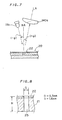
- Fig. 27 is a conceptual diagram showing a conventional image reading system employed in a wiring pattern inspecting apparatus.
- Light 2 emitted from a light source 1 is reflected by a half mirror 3, and applied to the surface of a printed circuit board 5.
- the printed circuit board 5 is provided with a wiring pattern 6 and a through hole 7, and reflected light 8 obtained by reflection of the light 2 on the surface thereof is imaged on a linear image sensor 9 through the half mirror 3 and an imaging lens 4.
- Fig. 28 shows exemplary incident photo-levels in the linear image sensor 9, which photo-levels correspond to a linear image along the line K - K in Fig. 27.
- the wiring pattern 6 has a large light reflectance since the same is made of a metal, and an incident photo-level corresponding to the wiring pattern 6 is also large.
- an incident photo-level from an insulating base 5a of the circuit board 5 is relatively small, while the light 2 is transmitted through the through hole 7 downwardly from the circuit board 5 and the photo-level therefrom is substantially zero.
- a threshold value TH it is possible to obtain the image of the wiring pattern 6 by discriminating the respective incident photo-levels using a threshold value TH.
- the conventional apparatus shown in Fig. 27 is on the premise that differences between the photo-levels from the respective regions 5a, 6 and 7 are large.
- the light reflectance on the surface of the wiring pattern 6 is not necessarily uniform, and the photo-level therefrom may fluctuate.
- the waveforms of the photo-levels are complicated by reflected light from an inner wall portion of the through hole 7, so that the boundary between respective images of the wiring pattern 6 and the through hole 7 is confused.
- the present invention is directed to an image reading system for reading an image of an object.
- the image reading system comprises: (a) an imaging optical system facing the object; (b) light source means provided in a part of an angular aperture of the imaging optical system and emitting illumination light toward the object, wherein the illumination light is reflected on the object to become a reflected light; and (c) image sensor means provided n the opposite side of the imaging optical system from the object, for receiving the reflected light through the imaging optical system to obtain an image of the object.
- Light from the light source means for reflective illumination is applied to the object through no half mirror etc. While a part of the light reflected by the object is eclipsed the light source means, the remaining part reaches the image sensor through the imaging optical system. Therefore, a considerable part of the light from the light source means is incident upon the image sensor, whereby image detection accuracy in the image sensor is improved.
- the light source means is so arranged as to be in contact with the optical axis of the imaging optical system, the reflected light reaching the image sensor without being eclipsed by the light source means is about 1/2 of the reflected light progressing toward an entrance pupil of the image detection part.
- an image reading system employable for reading respective images of a wiring pattern and a through hole of an printed board having first and second surfaces opposite to each other.
- the wiring pattern is formed on the first surface and the through hole is provided between the first and second surfaces.
- the image reading system comprises: (a) an imaging optical system facing the first surface of the printed board; (b) first light source means facing the first surface of the printed board to emit a first light having a first wavelength to the first surface of the printed board, wherein the first light is reflected on the wiring pattern to become a reflected light; (c) second light source means facing the second surface of the printed board to emit a second light having a second wavelength to the second surface of the printed board, wherein the second light is transmitted through the through hole to become a transmitted light which is overlapped with the reflected light to obtain a compound light entering the imaging optical system; (d) light splitter means for receiving the compound light having passed through the imaging optical system to split the compound light into the reflected light and the transmitted light; (e) first image sensor means for receiving the reflected light to obtain an image of the wiring pattern; and (f) second image sensor means for receiving the transmitted light to obtain an image of the through hole.
- the first light source means is adapted for reflective illumination of the wiring pattern, and the second light source means is adapted for transmitting illumination of the through hole.
- the first light from the first light source means and the second light that from the second light source means are applied to a common area on the printed board, whereby reflected light from the wiring pattern and transmitted light from the through hole form the spatially overlapped compound light.
- the first light for reflective illumination is different in wavelength from the second light for transmitting illumination.
- a wavelength separation mirror etc. as light splitter means, whereby the wiring pattern and the through hole can be simultaneously and correctly detected.
- Two types of light having different polarization directions may be employed in place of the two types of light having different wavelengths.
- the reflected light and the transmitted light obtained from the first light and the second light can be separated using a polarized beam splitter, for example.
- a telecentric lens system which is telecentric at least on the object side, is employed as the imaging optical system. Even if the through hole has a small diameter as a mini via hole, it is possible to correctly obtain an image using transmitted light therethrough.
- the image reading system comprises: (a) an imaging optical system; and (b) a selective reflection mirror covering whole of an angular aperture of the imaging optical system.
- the selective reflection mirror comprises a surface which consists of: a first region capable of reflecting a first light of a first optical character and capable of transmitting a second light of a second optical character; and a second region capable of reflecting the first and second lights.
- the angular aperture of the imaging optical system is divided into two parts with a boundary of the first and second regions.
- the image reading system further comprises: (c) first light source means provided out of the angular aperture of the imaging optical system, for emitting the first light toward the selective reflection mirror to direct the first light to the first surface of the printed board to obtain a reflected light through reflection of the first light on the wiring pattern; (d) second light source means provided on the second surface side, for emitting the second light toward the second surface of the printed board to obtain a transmitted light through transmittance of the second light through the through hole.
- first light source means provided out of the angular aperture of the imaging optical system, for emitting the first light toward the selective reflection mirror to direct the first light to the first surface of the printed board to obtain a reflected light through reflection of the first light on the wiring pattern
- second light source means provided on the second surface side, for emitting the second light toward the second surface of the printed board to obtain a transmitted light through transmittance of the second light through the through hole.
- the reflected light and the transmitted light are overlapped with each other to form a compound light.
- the compound light enters the selective reflection mirror and then passes through the imaging optical system.
- Also provided in the image reading system are; (e) light splitter means for receiving the compound light having passed through the imaging optical system to split the compound light into the reflected light and the transmitted light; (f) first image sensor means for receiving the reflected light to obtain an image of the wiring pattern; and (g) second image sensor means for receiving the transmitted light to obtain an image of the through hole.
- the image reading system comprises: (a) an imaging optical system; (b) a selective reflection mirror covering a part of an angular aperture of the imaging optical system and capable of reflecting a first light of a first optical character and capable of transmitting a second light of a second optical character; (c) first light source means provided out of the angular aperture of the imaging optical system, for emitting the first light toward the selective reflection mirror to direct the first light to the first surface of the printed board and to obtain a reflected light through reflection of the first light on the wiring pattern; and (d) second light source means provided on the second surface side, for emitting the second light toward the second surface of the printed board to obtain a transmitted light through transmittance of the second light through the through hole.
- the reflected light and the transmitted light are overlapped with each other to form a compound light.
- the compound light passes through a space in which the selective reflection mirror is provided and then enters the imaging optical system.
- both of a first part thereof passing through the selective reflection mirror and a second part bypassing the selective reflection mirror are received by the selective reflection mirror.
- Also provided in the image reading system are: (e) light splitter means for receiving the compound light having passed through the imaging optical system to split the compound light into the reflected light and the transmitted light; (f) first image sensor means for receiving the reflected light to obtain an image of the wiring pattern; and (g) second image sensor means for receiving the transmitted light to obtain an image of the through hole.
- the wiring pattern is detected using reflective illumination with the first light source means and the through hole is detected using transmitting illumination with the second light source means. Therefore, illuminations suitable for respective object images are effectuated in parallel, and two lights obtained through respective illuminations are separated from each other.
- the optical-amount of the light for transmitting illumination is fully usable in detection of the through hole image, and relatively large part of the light for regular reflection is usable in detection of the wiring pattern image.
- Anisotropy in the image detection signal of the through hole is not caused unlike the case where the light source for reflective illumination is arranged in the angular aperture of the imaging lens system.
- the present invention is applicable not only to appearance inspection of a printed circuit board, but also to image reading systems in various inspecting apparatuses such as that for appearance inspection of a magnetic disk or a semiconductor wafer.
- an object of the present invention is to provide an image reading system which increases the intensity of light received by an image sensor.
- Another object of the present invention is to provide an image reading system which can simultaneously and correctly detect respective images of a wiring pattern and a through hole in a printed circuit board.
- Another object of the present invention is to perform appearance inspection at high speed with high accuracy.
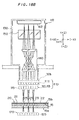
- Fig. 1A is a fragmented plan view showing a printed circuit board inspecting apparatus 10 in which an image reading system according to a first preferred embodiment of the present invention is incorporated
- Fig. 1B is a side elevational view thereof.
- the apparatus 10 comprises a lower housing 11 and an upper housing 12, and a movable table 13 is horizontally provided in the vicinity of an upper opening of the lower housing 11.
- the movable table 13 is formed by a rectangular frame 14 and a glass plate 15 mounted therein, and a bottom surface 15a of the glass plate 15 is coarsely-ground.
- a printed circuit board 20 is placed on a top surface 15b of the glass plate 15, and supported by the glass plate 15.
- the printed circuit board 20 has an insulating base plate 21 which is formed of glass epoxy, and a printed wiring pattern 22 of copper which is formed on one or each surface thereof.
- the printed wiring patter 22 has a wiring portion 23 and a land 24, and a through hole 25 passing through or penetrating the printed circuit board 20 is formed in the land 24.
- the frame 14 is slidable on a pair of guide rails 16, and a ball screw 17 extends in parallel with the guide rails 16.
- a ball nut 19 fixed to the frame 14 is fitted with the ball screw 17, so that the movable table 13 is moved in horizontal ( ⁇ Y) directions when the ball screw 17 is rotated by a motor 18.
- an image reading system 50 is provided in the interior of the upper housing 12.
- An optical head array 100 extending in horizontal ( ⁇ X) directions, is arranged in a central upper portion of the image reading system 50.
- This optical head array 100 comprises eight optical heads H0 to H7, which are supported by a support member 101 at regular intervals.
- the support member 101 is slidable on a guide member 102 in the directions ( ⁇ X), and the guide member 102 is fixed to a pair of side frame members 51a and 51b.
- the side frame members 51a and 51b are at fixed positions with respect to the housings 11 and 12.
- the support member 101 is coupled to a motor 103 through a ball nut (not shown) and a ball screw 104. When the motor 103 is rotated, therefore, the optical heads H0 to H7 are movable with the support member 101 in the directions ( ⁇ X).
- a light source 120 for transmitting illumination is arranged under the optical heads H0 to H7.
- This light source 120 is formed by a large number of infrared ray LEDs which are arrayed in the directions ( ⁇ X), and substantially functions as a linear light source.
- This light source 120 is supported by support rods 121 and 122 from the side frames 51.
- another light source 110 for reflective illumination is mounted on lower portions of the optical heads H0 to H7.
- the light source 110 comprises three one-dimensional arrays of red LEDs extending in the directions ( ⁇ X).
- Presser roller mechanisms 200A and 200B are provided in front and at the back of the optical head array 100.
- the front roller mechanism 200a comprising eight roller units 210A, is mounted on the side frames 51a and 51b through a shaft 201A.
- the rear roller mechanism 200B also comprising eight roller units 210B, is mounted on the side frames 51a and 51b through another shaft 201B.
- the roller units 200A and 200B have rubber rollers which are supported by swingable arms, and the rubber rollers and the arms are urged by springs.
- the roller mechanisms 200A and 200B are adapted to press the printed circuit board 20, which are fed under the same, to prevent the circuit board 20 from positional displacement and deflection.
- a pair of control switch panels 26 are mounted on top surfaces of both sides of the lower housing 11. These switch panels 26 are provided with identical switch groups, so that the switches can be easily controlled from either side of the housing 11.
- the upper housing 12 is provided therein with a data processing unit 300 for performing various data processing and operation control.
- the printed circuit board 20 is placed on the glass plate 15 in the state shown in Figs. 1A and 1B. Then either switch panel 26 is operated so that the motor 18 is positively rotated and the printed circuit board 20 is moved in the direction (+Y) with the movable table 13. The light sources 110 and 120 are turned on.
- the optical heads H0 to H7 read images of the wiring pattern 22 (Fig. 2) and the through hole 25 for each scanning line by reflective illumination from the light source 110 and transmitting illumination from the light source 120 respectively. Internal structures of the optical heads H0 to H7 for such reading are described later.
- the motor 103 is driven after complete movement of the printed circuit board 20 in the direction (+Y), thereby moving the overall optical heads H0 to H7 in the direction (+X). The amount of such movement is rendered half the interarray pitch of the optical heads H0 to H7.
- the motor 18 is reversely rotated to move the printed circuit board 20 in the direction (-Y), to read the images of the wiring pattern 22 and the through hole 25 by the optical heads H0 to H7.
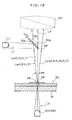
- Fig. 3A is a schematical side elevational view showing the internal structure of the optical head H0. While Fig. 3A illustrates only one optical head H0, the other optical heads H1 to H7 have the same structures.
- the optical head H0 has a casing 130, and the light source 110 for reflective illumination is suspended by support members 116 and 117 which are mounted on a lower portion of the casing 130.
- the light source 111 is called as "a light source for regular reflection"
- the light sources 112 and 113 are called as "light sources for irregular reflection”.
- the light sources 112 and 113 for irregular reflection are arranged at positions considerably separated from an optical axis LA of an imaging lens system 140 which is provided in the optical head H0, while the light source 111 for regular reflection is provided in such a position that its end surface is in contact with the optical axis LA.
- the imaging lens system 140 is adapted to form the images of the wiring pattern 22 and the through hole 25 of the printed circuit board 20 on CCD linear image sensors 161 and 162 respectively.
- the light sources 112 and 113 for irregular reflection are arranged in the exterior of the visible field or the angular aperture for the imaging, while the light source 111 for regular reflection is arranged in a part of the angular aperture.
- Light emitted from the light sources 111, 112 and 113 is applied toward an inspected area AR of the top surface of the printed circuit board 20, which is currently located immediately under the optical head H0.
- the light source 111 for regular reflection and the light sources 112 and 113 for irregular reflection are provided for reflective illumination for the reason that it is preferable to utilize both of regular reflection and irregular reflection from the wiring pattern 22 in order to correctly catch the image thereof, since the surface of the wiring pattern 22 does not necessarily define a mirror finished surface.
- the light sources 111, 112 and 113 are shaded on the imaging lens system 140 sides, i.e., in the upper sides in Figs. 1A and 1B.
- This light source 120 is provided on a line perpendicularly intersecting with the optical axis LA of the imaging lens system 140.
- This light source 120 emits the infrared light toward an area of the back surface of the printed circuit board 20 corresponding to the back side of the inspected area AR in a direction (+Z).
- the red light applied to the inspected area AR from the light sources 111, 112 and 113 for reflective illumination is reflected by the inspected area AR.
- part directed to the through hole 25 is penetrated or transmitted through the through hole 25.
- the reflected light and the transmitted light are spatially overlapped to become compound light, which in turn is directed to the optical head H0.
- luminous flux L0 outputted from the inspected area AR of the printed circuit board 20 and traveling toward a range of an entrance pupil of the imaging lens system 140. Only a part L a of the luminous flux L0, which corresponds to half luminous flux L0, reaches the imaging lens system 140 and another part L b corresponding to the remaining half is eclipsed or blocked by the light source 111 and the support member 116.
- each of the projection solid angle (the incoming angle of the compound light in the imaging lens system 140) ⁇ a of the effective luminous flux L a and the projection solid angle ⁇ b of the ineffective luminous flux L b is half the projection solid angle (the angular aperture) ⁇ 0 of the luminous flux L0.
- the effective luminous flux L a enters a cold mirror 150 through the imaging lens system 140.
- the cold mirror 150 is adapted to transmit only infrared light. Therefore, the red light contained in the effective luminous flux L a (i.e., the reflected light LR from the surface of the printed circuit board 20) is reflected by this mirror 150 to progress in the direction (+Y), and imaged on a photos-detective plane of the first CCD linear image sensor 161. Further, the infrared light contained in the effective luminous flux L a (i.e., the transmitted light LT through the through hole 25) is transmitted through the mirror 150 and imaged on a photo-detective plane of the second CCD linear image sensor 162.
- CCD linear image sensors 161 and 162 have CCD photo-electric converter cells which are one-dimensionally arrayed in the directions ( ⁇ X). Therefore, the first linear image sensor 161 detects a one-dimensional image of the surface of the printed circuit board 20 through the reflective illumination, while the second linear image sensor 162 detects a one-dimensional image of the through hole 25 through the transmitting illumination.
- the printed circuit board 20 and the optical head array 100 are relatively moved by the moving mechanism shown in Figs. 1A and 1B, whereby respective areas of the printed circuit board 20 are scanned and two-dimensional images of the wiring pattern 22 and the through hole 25 are obtained for respective areas on the printed board 20.
- Image signals obtained in the linear image sensors 161 and 162 are digitalized by circuits described below, and thereafter binarized using threshold values TH1 and TH2, as shown in Figs. 5A and 5B.
- Fig. 5A shows an exemplary image signal PS0 which is obtained in the first linear image sensor 161
- Fig. 5B shows an exemplary image signal HS0 which is obtained in the second linear image sensor 162.
- Fig. 3B is a typical front elevational view of the optical head H0 shown in Fig. 3A, and the first linear image sensor 161 is omitted in Fig. 3B for convenience of illustration.
- Optical paths in the optical head H0 are shown only as to the light transmitted through the through hole 25.
- a telecentric lens system which is telecentric on both sides being close to the printed circuit board 20 and the linear image sensors 161 and 162, is employed as the imaging lens system 140. Therefore, an imaging optical axis of the transmitted light from each through hole 25, which is in the visual field of this lens system 140, is parallel to the optical axis LA of the lens system 140 itself in both of the object side and the image-detection side of the lens system 140.
- the image reading system 50 having the aforementioned structure has the following advantages:
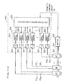
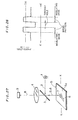
- Fig. 11A as combined with Fig. 11B is a block diagram showing an electrical structure of this embodiment.
- Wiring pattern image signals PS0 to PS7 and through hole image signals HS0 to HS7 obtained from the optical heads H0 to H7 are converted to digital signals by A-D converters 301, and thereafter supplied to binarizing circuits 302 and 303.
- Fig. 11C shows combination 304 of the binarizing circuits 302 and 303 corresponding to the optical head H0 in detail.
- the binarizing circuits 302 and 303 are formed by comparators 305 and 306, and the threshold values TH1 and TH2, which are held by registers 307 and 308, are supplied to the comparators 305 and 306, respectively.
- the comparators 305 and 306 compare the threshold values TH1 and TH2 with the digitalized image signals PS0 and HS0 (see Figs. 5A and 5B) respectively, to output binarized signals, which go high when the levels of the signals PS0 and HS0 are higher than the threshold values TH1 and TH2 while going low when the former are lower than the latter.
- the binarizing circuits 302 and 303 corresponding to the other optical heads H1 to H7 have similar structures, and the threshold values TH1 and TH2 from the registers 307 and 308 are commonly used for the respective pairs of the binarizing circuits 302 and 303.
- the binarized image signals thus obtained are supplied to a pattern inspection circuit 400.
- the pattern inspection circuit 400 constructs two-dimensional images of the wiring pattern 22 and the through hole 25 on the basis of these image signals, and determines whether the wiring pattern 22 and the through hole 25 are defective or non-defective in accordance with prescribed determination rule.
- the data processing unit 300 is also provided with a control circuit 310.
- the control circuit 310 supplies turn-on/off instructions to the light sources 110 and 120 through lighting circuits 311 and 312, and outputs driving control signals to the motors 18 and 103.
- the motor 18 is provided with a rotary encoder 18E, so that a motor rotation angle signal generated therein is delivered to the control circuit 310. This rotation angle signal defines data processing timing.
- the optical inspecting apparatus 10 shown in Figs. 1A and 1B accurately executes appearance inspection of the printed circuit board 20.
- visible light having a first wavelength may be employed for the light source 110 for reflective illumination in Figs. 3A and 3B
- visible light having a second wavelength may be employed for the light source 120 for transmitting illumination.
- the first and second wavelengths are different from each other.
- a dichroic mirror can be employed in place of the cold mirror 150.
- Such a dichroic mirror is implemented by a mirror which reflects the light of the first wavelength and transmits the light of the second wavelength.
- each of the light sources 110 and 120 combination of a white light source and a color filter may be employed.
- Fig. 13 illustrates an optical head H0 according to a second preferred embodiment of the present invention, which optical head H0 is employable in the image reading system 50 shown in Figs. 1A and 1B.
- this optical head H0 combination of white light sources 111A, 112A and 113A and an S-wave polarizing plate 119 is employed as a light source system for reflective illumination. Therefore, the reflective illumination light is an S-wave light, i.e., a light wave whose electric field vector is in the directions ( ⁇ X).
- the polarizing plate 119 is supported from the optical head H0 side by a support member (not shown).
- a light source system for transmitting illumination is formed by combination of a white light source 120A and a P-wave polarizing plate 129, and the P-wave polarizing plate 129 is supported from the white light source 120A side by a support member (not shown). Therefore, transmitting illumination light is a P-wave light, i.e., light wave whose electric field vector is in an XZ plane.
- Each illumination light is applied toward a printed circuit board 20 similarly to the case of Fig. 3A, and compound light from the circuit board 20 is incident upon a polarized beam splitter 151 through a telecentric lens system 140.
- the polarized beam splitter 151 reflects the S-wave and transmits the P-wave. Therefore, S-polarized reflected light LR containing image information of a wiring pattern 22 is imaged on a photoelectric converter plane of a linear image sensor 161, while P-polarized transmitted light LT containing image information of a through hole 25 is imaged on a photoelectric converter plane of another linear image sensor 162.
- the remaining structure is identical to that of Fig. 3A and the light source 112A is in contact with the optical axis of the imaging lens system 140.
- respective images of the wiring pattern 22 and the through hole 25 are simultaneously detected by the separate linear image sensors 161 and 162, whereby an effect similar to that of the system shown in Fig. 3A is attained.
- the light for reflective illumination may be P-polarized
- the light for transmitting illumination may be S-polarized.
- no polarizing plate may be employed.
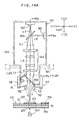
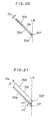
- Fig. 14A is a conceptional side elevational view of an optical head H0 according to a third preferred embodiment of the present invention and Fig. 14B is a conceptional front elevational view of the optical head H0 shown in Fig. 14A.
- the optical head H0 in Figs. 14A and 14B is comparable to the optical head shown in Fig. 3A and 3B in many points, the former has a characteristic structure as follows:
- the light source 111 for regular reflection is attached to the supporting member 116 in lateral direction (+Y) and is out of the angular aperture of the imaging lens system 140.
- the arrangement of the other light sources 112, 113 and 120 is the same as the first preferred embodiment.
- the light sources 111, 112 and 113 emit red light, while the light source 120 emits infrared light.
- the red light emitted from the light source 111 is reflected at a selective reflection mirror 30a and is directed to the inspected area AR.
- the red lights emitted from the light sources 112 and 113 are directly applied to the inspected area AR.
- the selective reflection mirror 30a is attached to the supporting members 116 and 117, and entirely covers the angular aperture ⁇ 0 (Fig. 15) of the imaging lens system 140.
- the selective reflection mirror 30a is inclined from the optical axis LA of the imaging lens system 140 by 45°.
- the mirror 30a comprises a plane substrate 31a made of transparent glass.
- the thickness of the plane substrate 31a is equal to or less than 10 mm.
- a major surface of the plane substrate 31a is conceptionally divided into two regions 33a and 34a, whose boundary line BL extends in the direction perpendicular to the drawing sheet.
- the mirror 30a is positioned so that the boundary line BL substantially crosses the optical axis LA at a right angle, i.e., 90°.
- the boundary line BL therefore, substantially divides the angular aperture ⁇ 0 into two equal parts.
- the first region 33a is a cold mirror region which substantially transmits light having wavelength longer than a characteristic critical wavelength but substantially reflects light having wavelength shorter than the critical wavelength.
- the critical wavelength thereof is about 700 nm.
- the light is reflected at the first region 33a.
- the light source 111 for regular reflection faces the fist region 33a, and the red light L1 (Fig. 7) emitted from the light source 111 is reflected on the first regoin 33a to be directed to the inspected area AR of a printed circuit board 20.
- the red lights from the light sources 112 and 113 for irregular reflection are directly applied to the inspected area AR. These red lights are reflected on the inspected area AR to become reflected light LR containing image information of the wiring pattern.
- the infrared light emitted from the light source 120 for transmitting illumination is incident on the back surface of the printed circuit board 20, and a part thereof entering the through hole 25 passes through the through hole 25 to become transmitted light containing image information of the through hole 25.
- These reflected light and the transmitted light are spatially overlapped to become compound light L RT , which is incident on the mirror 30a.
- the reflected light incident on the angular aperture or the entrance pupil of the imaging lens system 140 includes regular reflection light LR1 and irregular reflection light LR2.
- the regular reflection light LR1 is obtained through regular reflection of the light from the light source 111 on the inspected region AR
- irregular reflection light LR2 is obtained through irregular reflection of the lights from the light sources 112 and 113 on the inspected region AR.
- the compound light L RT In positional arrangement of the compound light L RT travelling from the inspected area AR to the angular aperture of the imaging lens system 140, the compound light L RT consists of a first portion L RT1 incident on the first region 33a of the mirror 30a and a second portion L RT2 incident on the second region 34a.
- the irregular reflection light LR2 is included in both of the first portion L RT1 and the second portion L RT2 , while the regular reflection light LR1 is included only in the second region L RT2 .
- the transmitted light LT from the light source 120 is included both of the first portion L RT1 and the second portion L RT2 .
- the transmitted light LT included in the compound light L RT is transmitted through the mirror 30a to enter the upper space of the mirror 30a regardless of whether the same is incident on the first region 33a or the second region 34a.
- the regular reflected light LR1 is transmitted through the second regoin 34a and enters the upper space of the mirror 30a.
- a portion L f passing through the right side of the optical axis LA in Fig. 14A includes the transmitted light LT and the reflected light LR, while another portion L g passing through the left side of the optical axis LA includes only the reflected light LR.
- the compound light L c having these components are incident on a cold mirror 150 through the imaging lens system 140.
- the cold mirror 150 is such a mirror that only infrared light is transmitted therethrough. Therefore, as is in the first preferred embodiment, the reflected red light LR included in the compound light L c is further reflected on the cold mirror 150 and is incident on a CCD linear sensor array 161.
- the transmitted infrared light LT is transmitted through the mirror 30a and is incident on another CCD linear sensor array 162.
- Photoelectric conversion of the lights incident on the linear sensor array 161 and 162 and electronic processing in image processing circuits provided in the rear stage of the sensors 161 and 162 are similar to the first preferred embodiment and description thereof is omitted here.
- a telecentric lens system is employed for the imaging lens system 140, as in the first and second preferred embodiments.
- optical head H0 shown in Figs. 14a, 14B and 15 and the inspection device employing the same have the following characteristic advantages in addition to the generic advantages of the present invention.
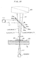
- Figs. 18A, 18B and 19 are a schematic side view, a schematic front view and a schematic view showing major portion of an optical head H0 according to a fourth preferred embodiment of the present invention, respectively. In the folowing description, only the difference between the third and fourth preferred embodiment is described.
- the optical head H0 comprises a selective reflection mirror 30b under an imaging lens system 140.
- the mirror 30b has a plane substrate 31b made of transparent glass, on which a thin film 35b is deposited.
- the thin film 35b serves as a selective light-reflection layer.
- the thickness of the plane subatrate 31b is 50 ⁇ m or less.
- the material and the thickness of the thin film 35b are the same as the thin film 35a in the third preferred embodiment. Accordingly, respective regions on the mirror 30b reflect the light for reflective illumination and transmit the light for transmitting illumination.
- the mirror 30b is inclined from the optical axis LA of the imaging lens system 140 by 45° and a light source 111 for regular reflection is arranged to face the mirror 30b.
- An edge EP of the mirror 30b is located on the optical axis LA and the mirror 30b covers about half of the angular aperture of the imaging lens system 140.
- the right half portion Lf (Fig. 18A) and the left half portion Lg of the compound light have the same components as the third preferred embodiment.
- the compound light going out of the imaging lens system 140 is divided into reflected light LR and transmitted light LT with a dichroic mirror 150 and these lights LR and LT are detected by CCD linear image sensors 161 and 162, respectively. Respective images of the wiring pattern 22 and the through hole 25 are detected through this process and are delivered to inspection circuits. Therefore, this fourth preferred embodiment has advantages similar to the the third preferred embodiment.
- the edge surface 30E (Fig. 20) may be perpendicular to the photo-reflective major surface of the mirror 30b.
- the edge surface 30E is processed to a wedge of 45 ° so that the edge surface 30E is in parallell to the optical axis LA.
- the thickness D31 of the substrate 30b is made thin regardless of whether the edge surface 30E is shaped into a wedge or not. If the thickness D31 is extremely large as shown in Fig. 22, the light path of the transmitted light passing through a point Q0 is changed to a high degree due to refraction in the substrate 30b and, as a result, a convergent point P1 of the light passing through the right side of the optical axis LA is largely deviated from a point P2 at which the light passing through the left side of the optical axis LA.
- the thickness D31 is so determined that the distance between the points P1 and P2 is equal to or less than a value ⁇ y (not shown) , where the value ⁇ y is a predetermined allowable limit of the error in conversion of light on the photo-electric conversion plane of the linear image sensor 162.
- Figs. 23A, 23B and 24 are a schematic side view, a schematic front view and a schematic view showing major portion of an optical head H0 according to a fifth preferred embodiment of the present invention, respectively.
- the third preferred embodiment is similar to the third preferred embodiment, difference therebetween is in that light for reflective illumination and that for transmitting illumination are separated from each other through distinction between polarized lights rather than distinction of wavelength.
- a light source system for reflective illumination comprises combination of white light sources 111A, 112B and 113B and S-wave polarizing plates 119. Accordingly, the light for reflective illumination is S-wave, i.e., light whose elecrtic field vector is in ( ⁇ X) directions.
- the polarizing plates 119 are supported from the optical head H0 side through supporting members (not shown).
- a light source system 120 for transmitting illumination consists of white light sources 125A and P-wave polarizing plate 129.
- the P-wave polarizing plate 129 is supported in the system 120 through supporting members (not shown). Accordingly, the light for transmitting illumination is P-wave, i.e, light whose electric vector is in XZ-plane.
- a mirror 30c provided under an imaging lens system 140 covers the whole area of the angular aperture ⁇ 0 of the imaging lens system 140.
- the morror 30c comprises a plane substrate 31c made of transparent glass as shown in Fig. 24, and a major surface of the plane substrate 31c is conceptionally divided into a first region 33c and a second region 34c similarly to the third preferred embodiment shown in Figs. 14A, 14B and 15.
- the boundary line BL between the first regon 33c and the second region 34c crosses the optical axis LA of the imaging lens system 140 at a right angle. Accordingly , the boundary line BL of the regions 33c and 34c substantially divides the angular aperture ⁇ 0 into equal two parts.
- the first region 33c is provided thereon with a thin film 35c for splitting light into respective polalized components.
- the first region 33c transmits P-polarized light and reflects S-polarized light. Consequently, the light from the light source 111A for regular reflection is reflected on the first region 33c to be applied to the surface of a printed board 20.
- the S-polarized lights from the light sources 111A, 112A and 113A are reflected on the wiring pattern 22, while the P-polarized light from the light source 120 transmitted through a through hole 25.
- a compound light L RT which is a combination the reflected light and the transmitted light, enters the mirror 30c.
- Optical character and function of the mirror 30c is understood by rewriting "the lights of respective wavelength” in the description of the third preferred embodiment to "the lights of respective polarizations”.
- the imaging lens system 140 receives the compound light consisting of the S-polarized light and the P-polarized light.
- the compound light enters a polarized beam splitter 151.
- the polarized beam splitter 151 transmits S-wave and reflects P-wave. Consequently, the S-polarized reflected light LR (Fig. 23A) having image information of the wring pattern 22 is imaged on the photo-electric conversion plane of a linear image sensor 161, while the P-polarized reflected light LT having image information of the through hole 25 is imaged on the photo-electric conversion plane of another linear image sensor 162.
- the other construction is the same with the third preferred embodiment.
- the fifth preferred embodiment has advantages similar to the third and fourth preferred embodiments, which advantages includs improvement in utilization efficiency of photo-amount of lights.
- the light for reflective illumination may be P- polarized light, while the light for transmitting illumination may be S-polarized light.
- polarizing plates 119 and 129 may be omitted.
- a sixth preferred embodiment is shown in Figs. 25A, 25B and 26.
- An optical head H0 according to the sixth preferred embodiment is a combination of the fourth and fifth preferred embodiments. That is, two kinds of lights are splitted through the technique of polarized light splitting, while the optical head H0 is provided with a mirror 30d having the same shape and located at the same position as the mirror 30b in Fig. 19.
- the mirror 30d comprises a transparent glass substrate on which a thin film 35d for polarization splitting is formed.
- An edge EP of the mirror 30d crosses the optical axis LA of an imaging lens system at a right angle.
Landscapes
- Physics & Mathematics (AREA)
- General Physics & Mathematics (AREA)
- Health & Medical Sciences (AREA)
- Engineering & Computer Science (AREA)
- Immunology (AREA)
- Computer Vision & Pattern Recognition (AREA)
- General Health & Medical Sciences (AREA)
- Analytical Chemistry (AREA)
- Chemical & Material Sciences (AREA)
- Pathology (AREA)
- Life Sciences & Earth Sciences (AREA)
- Biochemistry (AREA)
- Electromagnetism (AREA)
- Toxicology (AREA)
- General Engineering & Computer Science (AREA)
- Length Measuring Devices By Optical Means (AREA)
- Investigating Materials By The Use Of Optical Means Adapted For Particular Applications (AREA)
- Image Input (AREA)
- Supply And Installment Of Electrical Components (AREA)
Applications Claiming Priority (6)
| Application Number | Priority Date | Filing Date | Title |
|---|---|---|---|
| JP142890/90 | 1990-05-30 | ||
| JP14289090A JPH0434346A (ja) | 1990-05-30 | 1990-05-30 | イメージ読取りシステム |
| JP142889/90 | 1990-05-30 | ||
| JP2142889A JPH0434345A (ja) | 1990-05-30 | 1990-05-30 | プリント基板検査装置のためのイメージ読取りシステム |
| JP3335491U JPH04120312U (ja) | 1991-04-11 | 1991-04-11 | プリント基板検査装置のためのイメージ読取り装置 |
| JP33354/91 | 1991-04-11 |
Publications (3)
| Publication Number | Publication Date |
|---|---|
| EP0459489A2 true EP0459489A2 (fr) | 1991-12-04 |
| EP0459489A3 EP0459489A3 (en) | 1992-08-19 |
| EP0459489B1 EP0459489B1 (fr) | 1997-01-22 |
Family
ID=27288042
Family Applications (1)
| Application Number | Title | Priority Date | Filing Date |
|---|---|---|---|
| EP91108874A Expired - Lifetime EP0459489B1 (fr) | 1990-05-30 | 1991-05-29 | Procédé de lecture d'une image surface à examiner et système de lecture d'image utilisable dans ledit procédé |
Country Status (3)
| Country | Link |
|---|---|
| US (1) | US5197105A (fr) |
| EP (1) | EP0459489B1 (fr) |
| DE (1) | DE69124288T2 (fr) |
Cited By (8)
| Publication number | Priority date | Publication date | Assignee | Title |
|---|---|---|---|---|
| EP0562614A3 (en) * | 1992-03-26 | 1994-08-24 | Sumitomo Wiring Systems | Method and apparatus for inspecting a solderless terminal by image processing |
| EP0718624A3 (fr) * | 1994-12-19 | 1997-07-30 | At & T Corp | Procédé et appareil pour l'illumination des matériaux translucides ou semitransparents |
| EP0819933A3 (fr) * | 1996-07-16 | 1998-06-17 | Orbot Instruments Limited | Procédé et dispositif d'inspection optique |
| DE19739885A1 (de) * | 1997-09-11 | 1999-03-18 | Bernd Klose | Komparativer Oberflächenqualifizierer |
| WO2000070360A1 (fr) * | 1999-05-14 | 2000-11-23 | Mv Research Limited | Systeme d'inspection de trous d'interconnexion microscopiques |
| WO2012128920A1 (fr) * | 2011-03-21 | 2012-09-27 | Federal-Mogul Corporation | Système imageur multi-spectre et son utilisation avec un procédé d'inspection de surfaces |
| CN105277574A (zh) * | 2014-07-22 | 2016-01-27 | 牧德科技股份有限公司 | 应用重复曝光的多曝光影像混合的检测方法 |
| TWI821348B (zh) * | 2019-08-01 | 2023-11-11 | 由田新技股份有限公司 | 量測孔狀結構的自動光學檢測系統 |
Families Citing this family (32)
| Publication number | Priority date | Publication date | Assignee | Title |
|---|---|---|---|---|
| US5365084A (en) * | 1991-02-20 | 1994-11-15 | Pressco Technology, Inc. | Video inspection system employing multiple spectrum LED illumination |
| DE69329186T2 (de) * | 1993-01-01 | 2001-04-05 | Canon Kk | Bildlesevorrichtung |
| KR100269731B1 (ko) * | 1993-07-15 | 2000-10-16 | 하루타 히로시 | 영상 프로세서용 광원장치 |
| EP0666685B1 (fr) * | 1994-02-03 | 2001-05-16 | Canon Kabushiki Kaisha | Dispositif de formation d'images |
| JP3358099B2 (ja) * | 1994-03-25 | 2002-12-16 | オムロン株式会社 | 光学式センサ装置 |
| WO1995035506A2 (fr) * | 1994-06-17 | 1995-12-28 | Kensington Laboratories, Inc. | Lecteur de marques gravees |
| US5610710A (en) * | 1996-05-28 | 1997-03-11 | International Business Machines Corporation | Dual mode illumination system for optical inspection |
| US5982493A (en) * | 1998-06-02 | 1999-11-09 | Motorola, Inc. | Apparatus and method for acquiring multiple images |
| JP3330089B2 (ja) * | 1998-09-30 | 2002-09-30 | 株式会社大協精工 | ゴム製品の検査方法及び装置 |
| JP2004127220A (ja) * | 2002-10-01 | 2004-04-22 | Aisin Engineering Kk | コード読取装置 |
| JP4265206B2 (ja) * | 2002-11-27 | 2009-05-20 | 株式会社 東北テクノアーチ | 非接触導電率測定システム |
| JP4166585B2 (ja) * | 2003-01-20 | 2008-10-15 | 株式会社サキコーポレーション | 外観検査装置および外観検査方法 |
| JP4166587B2 (ja) * | 2003-01-24 | 2008-10-15 | 株式会社サキコーポレーション | 外観検査装置および体積検査方法 |
| US6963396B2 (en) * | 2003-06-27 | 2005-11-08 | Meyer Tool, Inc. | Light hole inspection system for engine component |
| JP2005181014A (ja) * | 2003-12-17 | 2005-07-07 | Hitachi Software Eng Co Ltd | 画像読取装置及び画像読取方法 |
| DE102004029212B4 (de) * | 2004-06-16 | 2006-07-13 | Leica Microsystems Semiconductor Gmbh | Vorrichtung und Verfahren zur optischen Auf- und/oder Durchlichtinspektion von Mikrostrukturen im IR |
| US20070115460A1 (en) * | 2005-11-21 | 2007-05-24 | Capaldo Kevin P | Method for examining molds and apparatus for accomplishing the same |
| US8509272B2 (en) | 2009-06-10 | 2013-08-13 | Lee Laser, Inc. | Laser beam combining and power scaling device |
| GB201017506D0 (en) * | 2010-10-15 | 2010-12-01 | Rolls Royce Plc | Hole inspection |
| JP5907180B2 (ja) * | 2012-02-10 | 2016-04-26 | 株式会社島津製作所 | 太陽電池セルの検査装置および太陽電池セルの処理装置 |
| US8902428B2 (en) * | 2012-03-15 | 2014-12-02 | Applied Materials, Inc. | Process and apparatus for measuring the crystal fraction of crystalline silicon casted mono wafers |
| JP2015175607A (ja) * | 2014-03-13 | 2015-10-05 | 株式会社Screenホールディングス | 画像取得装置および検査装置 |
| DE102015113451A1 (de) * | 2015-08-14 | 2017-02-16 | Visimation GmbH Bildverarbeitung für die Automation | Optische Messanordnung |
| US10145999B2 (en) | 2016-01-28 | 2018-12-04 | Apple Inc. | Polarizing beamsplitter that passes s-polarization and reflects p-polarization |
| US10545096B1 (en) * | 2018-10-11 | 2020-01-28 | Nanotronics Imaging, Inc. | Marco inspection systems, apparatus and methods |
| US10915992B1 (en) | 2019-08-07 | 2021-02-09 | Nanotronics Imaging, Inc. | System, method and apparatus for macroscopic inspection of reflective specimens |
| US11593919B2 (en) | 2019-08-07 | 2023-02-28 | Nanotronics Imaging, Inc. | System, method and apparatus for macroscopic inspection of reflective specimens |
| US11435298B2 (en) | 2020-07-24 | 2022-09-06 | Hewlett Packard Enterprise Development Lp | Circuit board anomaly indication |
| CN113791090A (zh) * | 2021-09-14 | 2021-12-14 | 慧镕电子系统工程股份有限公司 | 一种回收电路板焊接缺陷快速检定系统及方法 |
| US11714051B2 (en) * | 2021-11-30 | 2023-08-01 | Mitutoyo Corporation | Metrology system configured to measure apertures of workpieces |
| KR102708531B1 (ko) * | 2021-12-13 | 2024-09-24 | 한국기계연구원 | 다중 굴절률층을 이용한 빔스플리터 및 이를 포함하는 불량소자 검출장치 |
| US12204226B2 (en) * | 2023-05-25 | 2025-01-21 | Mitutoyo Corporation | Metrology system configured to illuminate and measure apertures of workpieces |
Family Cites Families (13)
| Publication number | Priority date | Publication date | Assignee | Title |
|---|---|---|---|---|
| DD209294A1 (de) * | 1982-08-02 | 1984-04-25 | Hans Tandler | Beleuchtungseinrichtung, vorzugsweise fuer auflichtmikroskope |
| US4538909A (en) * | 1983-05-24 | 1985-09-03 | Automation Engineering, Inc. | Circuit board inspection apparatus and method |
| DE3422395A1 (de) * | 1983-06-16 | 1985-01-17 | Hitachi, Ltd., Tokio/Tokyo | Verfahren und vorrichtung zum ermitteln von verdrahtungsmustern |
| GB8320016D0 (en) * | 1983-07-25 | 1983-08-24 | Lloyd Doyle Ltd | Apparatus for inspecting printed wiring boards |
| GB2143944B (en) * | 1983-07-25 | 1986-12-03 | Lloyd Doyle Ltd | Inspection of printed wiring boards |
| JPH0617777B2 (ja) * | 1984-06-02 | 1994-03-09 | 大日本スクリーン製造株式会社 | プリント配線板の撮像方法 |
| KR900001976B1 (ko) * | 1984-11-01 | 1990-03-30 | 가부시끼가이샤 히다찌세이사꾸쇼 | 다수 개의 패턴 발생기를 포함하는 패턴 검사 장치 |
| EP0195161B1 (fr) * | 1985-03-14 | 1993-09-15 | Nikon Corporation | Appareil et procédé d'inspection automatique d'objets et d'identification ou de reconnaissance de leurs parties connues et inconnues, y compris des défauts et similaires |
| US4794647A (en) * | 1985-04-08 | 1988-12-27 | Northern Telecom Limited | Automatic optical inspection system |
| DE3769000D1 (de) * | 1986-04-23 | 1991-05-08 | Siemens Ag | Vorrichtung zur auflichtbeleuchtung. |
| US4922308A (en) * | 1986-06-27 | 1990-05-01 | Hitachi, Ltd. | Method of and apparatus for detecting foreign substance |
| EP0263473B1 (fr) * | 1986-10-03 | 1994-07-27 | Omron Tateisi Electronics Co. | Appareil pour l'inspection d'un dispositif électronique encapsulé |
| US4845558A (en) * | 1987-12-03 | 1989-07-04 | Kla Instruments Corporation | Method and apparatus for detecting defects in repeated microminiature patterns |
-
1991
- 1991-05-29 US US07/706,801 patent/US5197105A/en not_active Expired - Fee Related
- 1991-05-29 EP EP91108874A patent/EP0459489B1/fr not_active Expired - Lifetime
- 1991-05-29 DE DE69124288T patent/DE69124288T2/de not_active Expired - Fee Related
Cited By (13)
| Publication number | Priority date | Publication date | Assignee | Title |
|---|---|---|---|---|
| EP0562614A3 (en) * | 1992-03-26 | 1994-08-24 | Sumitomo Wiring Systems | Method and apparatus for inspecting a solderless terminal by image processing |
| US5377278A (en) * | 1992-03-26 | 1994-12-27 | Sumitomo Wiring Systems, Ltd. | Method and apparatus for inspecting a solderless terminal by image processing |
| EP0718624A3 (fr) * | 1994-12-19 | 1997-07-30 | At & T Corp | Procédé et appareil pour l'illumination des matériaux translucides ou semitransparents |
| EP0819933A3 (fr) * | 1996-07-16 | 1998-06-17 | Orbot Instruments Limited | Procédé et dispositif d'inspection optique |
| US5892579A (en) * | 1996-07-16 | 1999-04-06 | Orbot Instruments Ltd. | Optical inspection method and apparatus |
| DE19739885A1 (de) * | 1997-09-11 | 1999-03-18 | Bernd Klose | Komparativer Oberflächenqualifizierer |
| WO2000070360A1 (fr) * | 1999-05-14 | 2000-11-23 | Mv Research Limited | Systeme d'inspection de trous d'interconnexion microscopiques |
| US6697154B2 (en) | 1999-05-14 | 2004-02-24 | Mv Research Limited | Microvia inspection system |
| WO2012128920A1 (fr) * | 2011-03-21 | 2012-09-27 | Federal-Mogul Corporation | Système imageur multi-spectre et son utilisation avec un procédé d'inspection de surfaces |
| US9128036B2 (en) | 2011-03-21 | 2015-09-08 | Federal-Mogul Corporation | Multi-spectral imaging system and method of surface inspection therewith |
| CN105277574A (zh) * | 2014-07-22 | 2016-01-27 | 牧德科技股份有限公司 | 应用重复曝光的多曝光影像混合的检测方法 |
| CN105277574B (zh) * | 2014-07-22 | 2018-04-03 | 牧德科技股份有限公司 | 应用重复曝光的多曝光影像混合的检测方法 |
| TWI821348B (zh) * | 2019-08-01 | 2023-11-11 | 由田新技股份有限公司 | 量測孔狀結構的自動光學檢測系統 |
Also Published As
| Publication number | Publication date |
|---|---|
| EP0459489B1 (fr) | 1997-01-22 |
| DE69124288D1 (de) | 1997-03-06 |
| EP0459489A3 (en) | 1992-08-19 |
| DE69124288T2 (de) | 1997-05-07 |
| US5197105A (en) | 1993-03-23 |
Similar Documents
| Publication | Publication Date | Title |
|---|---|---|
| US5197105A (en) | Method of reading optical image of inspected surface and image reading system employabale therein | |
| US6175645B1 (en) | Optical inspection method and apparatus | |
| US5748305A (en) | Method and apparatus for particle inspection | |
| US5774224A (en) | Linear-scanning, oblique-viewing optical apparatus | |
| KR19980042882A (ko) | 이물질 검사를 위한 방법 및 장치 | |
| JPH07111403B2 (ja) | 光学式検査装置および検査方法 | |
| JP2001155160A (ja) | 電子部品の外観検査装置 | |
| JP2512093B2 (ja) | 異物検出装置及び方法 | |
| JP2512059B2 (ja) | 異物検出方法及びその装置 | |
| US5414513A (en) | Printed circuit inspection system utilizing interference fringes | |
| JPH0156682B2 (fr) | ||
| JPS61104242A (ja) | 半導体ウェハ異物検査装置 | |
| JPH03102249A (ja) | 異物検出方法およびその装置 | |
| JP2008051666A (ja) | 欠陥検査装置 | |
| JPS6280507A (ja) | 路面ひびわれ測定方法 | |
| JPH09318553A (ja) | 基板の検査方法 | |
| JPH0621877B2 (ja) | 表面状態測定装置 | |
| JP2001108638A (ja) | 欠陥検査装置 | |
| JPH10132704A (ja) | 光学検査装置 | |
| JPH0434346A (ja) | イメージ読取りシステム | |
| JP3680959B2 (ja) | パターンチェッカ | |
| JPH04120312U (ja) | プリント基板検査装置のためのイメージ読取り装置 | |
| JP2830430B2 (ja) | 異物検査装置 | |
| JPS5899736A (ja) | 表面欠陥検出装置 | |
| JPS62188943A (ja) | 表面状態測定装置 |
Legal Events
| Date | Code | Title | Description |
|---|---|---|---|
| PUAI | Public reference made under article 153(3) epc to a published international application that has entered the european phase |
Free format text: ORIGINAL CODE: 0009012 |
|
| AK | Designated contracting states |
Kind code of ref document: A2 Designated state(s): DE FR GB |
|
| PUAL | Search report despatched |
Free format text: ORIGINAL CODE: 0009013 |
|
| AK | Designated contracting states |
Kind code of ref document: A3 Designated state(s): DE FR GB |
|
| 17P | Request for examination filed |
Effective date: 19921125 |
|
| 17Q | First examination report despatched |
Effective date: 19950220 |
|
| GRAG | Despatch of communication of intention to grant |
Free format text: ORIGINAL CODE: EPIDOS AGRA |
|
| GRAH | Despatch of communication of intention to grant a patent |
Free format text: ORIGINAL CODE: EPIDOS IGRA |
|
| GRAH | Despatch of communication of intention to grant a patent |
Free format text: ORIGINAL CODE: EPIDOS IGRA |
|
| GRAA | (expected) grant |
Free format text: ORIGINAL CODE: 0009210 |
|
| AK | Designated contracting states |
Kind code of ref document: B1 Designated state(s): DE FR GB |
|
| ET | Fr: translation filed | ||
| REF | Corresponds to: |
Ref document number: 69124288 Country of ref document: DE Date of ref document: 19970306 |
|
| PLBE | No opposition filed within time limit |
Free format text: ORIGINAL CODE: 0009261 |
|
| STAA | Information on the status of an ep patent application or granted ep patent |
Free format text: STATUS: NO OPPOSITION FILED WITHIN TIME LIMIT |
|
| 26N | No opposition filed | ||
| PGFP | Annual fee paid to national office [announced via postgrant information from national office to epo] |
Ref country code: FR Payment date: 20000510 Year of fee payment: 10 |
|
| PGFP | Annual fee paid to national office [announced via postgrant information from national office to epo] |
Ref country code: GB Payment date: 20000524 Year of fee payment: 10 |
|
| PGFP | Annual fee paid to national office [announced via postgrant information from national office to epo] |
Ref country code: DE Payment date: 20000529 Year of fee payment: 10 |
|
| PG25 | Lapsed in a contracting state [announced via postgrant information from national office to epo] |
Ref country code: GB Free format text: LAPSE BECAUSE OF NON-PAYMENT OF DUE FEES Effective date: 20010529 |
|
| GBPC | Gb: european patent ceased through non-payment of renewal fee |
Effective date: 20010529 |
|
| PG25 | Lapsed in a contracting state [announced via postgrant information from national office to epo] |
Ref country code: FR Free format text: LAPSE BECAUSE OF NON-PAYMENT OF DUE FEES Effective date: 20020131 |
|
| PG25 | Lapsed in a contracting state [announced via postgrant information from national office to epo] |
Ref country code: DE Free format text: LAPSE BECAUSE OF NON-PAYMENT OF DUE FEES Effective date: 20020301 |