EP0459918A1 - Leitfähiges Substrat und seine Verwendung in den Druckmedien - Google Patents
Leitfähiges Substrat und seine Verwendung in den Druckmedien Download PDFInfo
- Publication number
- EP0459918A1 EP0459918A1 EP19910420158 EP91420158A EP0459918A1 EP 0459918 A1 EP0459918 A1 EP 0459918A1 EP 19910420158 EP19910420158 EP 19910420158 EP 91420158 A EP91420158 A EP 91420158A EP 0459918 A1 EP0459918 A1 EP 0459918A1
- Authority
- EP
- European Patent Office
- Prior art keywords
- conductive
- conductive layer
- vinyl monomer
- type copolymer
- weight
- Prior art date
- Legal status (The legal status is an assumption and is not a legal conclusion. Google has not performed a legal analysis and makes no representation as to the accuracy of the status listed.)
- Granted
Links
Images
Classifications
-
- G—PHYSICS
- G03—PHOTOGRAPHY; CINEMATOGRAPHY; ANALOGOUS TECHNIQUES USING WAVES OTHER THAN OPTICAL WAVES; ELECTROGRAPHY; HOLOGRAPHY
- G03G—ELECTROGRAPHY; ELECTROPHOTOGRAPHY; MAGNETOGRAPHY
- G03G5/00—Recording-members for original recording by exposure, e.g. to light, to heat or to electrons; Manufacture thereof; Selection of materials therefor
- G03G5/10—Bases for charge-receiving or other layers
- G03G5/105—Bases for charge-receiving or other layers comprising electroconductive macromolecular compounds
- G03G5/107—Bases for charge-receiving or other layers comprising electroconductive macromolecular compounds the electroconductive macromolecular compounds being cationic
-
- G—PHYSICS
- G03—PHOTOGRAPHY; CINEMATOGRAPHY; ANALOGOUS TECHNIQUES USING WAVES OTHER THAN OPTICAL WAVES; ELECTROGRAPHY; HOLOGRAPHY
- G03G—ELECTROGRAPHY; ELECTROPHOTOGRAPHY; MAGNETOGRAPHY
- G03G5/00—Recording-members for original recording by exposure, e.g. to light, to heat or to electrons; Manufacture thereof; Selection of materials therefor
- G03G5/10—Bases for charge-receiving or other layers
- G03G5/104—Bases for charge-receiving or other layers comprising inorganic material other than metals, e.g. salts, oxides, carbon
-
- Y—GENERAL TAGGING OF NEW TECHNOLOGICAL DEVELOPMENTS; GENERAL TAGGING OF CROSS-SECTIONAL TECHNOLOGIES SPANNING OVER SEVERAL SECTIONS OF THE IPC; TECHNICAL SUBJECTS COVERED BY FORMER USPC CROSS-REFERENCE ART COLLECTIONS [XRACs] AND DIGESTS
- Y10—TECHNICAL SUBJECTS COVERED BY FORMER USPC
- Y10T—TECHNICAL SUBJECTS COVERED BY FORMER US CLASSIFICATION
- Y10T428/00—Stock material or miscellaneous articles
- Y10T428/24—Structurally defined web or sheet [e.g., overall dimension, etc.]
- Y10T428/24802—Discontinuous or differential coating, impregnation or bond [e.g., artwork, printing, retouched photograph, etc.]
- Y10T428/24917—Discontinuous or differential coating, impregnation or bond [e.g., artwork, printing, retouched photograph, etc.] including metal layer
-
- Y—GENERAL TAGGING OF NEW TECHNOLOGICAL DEVELOPMENTS; GENERAL TAGGING OF CROSS-SECTIONAL TECHNOLOGIES SPANNING OVER SEVERAL SECTIONS OF THE IPC; TECHNICAL SUBJECTS COVERED BY FORMER USPC CROSS-REFERENCE ART COLLECTIONS [XRACs] AND DIGESTS
- Y10—TECHNICAL SUBJECTS COVERED BY FORMER USPC
- Y10T—TECHNICAL SUBJECTS COVERED BY FORMER US CLASSIFICATION
- Y10T428/00—Stock material or miscellaneous articles
- Y10T428/25—Web or sheet containing structurally defined element or component and including a second component containing structurally defined particles
- Y10T428/252—Glass or ceramic [i.e., fired or glazed clay, cement, etc.] [porcelain, quartz, etc.]
Definitions
- the present invention pertains to conductive substrates applicable to recording processes, and more particularly, to conductive substrates for which the conductive layer thereof exhibits enduring conductive characteristics and excellent resistance to water.
- Conductive substrates are conventionally used for supporting the image recording layer in electrostatic recording media, photosensitive media used for electrophotography, and other types of printing and copying media.
- Electrostatic copying and printing methods which employ media incorporating a conductive substrate and devices which employ such methods have enjoyed widespread popularity, including facsimile devices, printing and reproduction devices for mechanical drawings, schematic diagrams, etc., devices for printing proofsheets for use in proofreading for newspapers and other publications, and devices for copying official documents and the like. Furthermore, in recent years, refinements in electrostatic copying and printing methods have made production of multicolor copies and prints possible, which has been put to use for diverse applications including the field of design in general, as well as for production of advertisement and promotional fliers, programs for plays, sporting events and the like, and various other applications.
- the electrostatic recording medium prepared as described above was found to be satisfactory.
- the employed electrolyte material containing amine group is water soluble, exposure to rain or moisture resulted in solublization thereof, with subsequent peeling of the conductive layer, and hence, of the electrostatically printed image. As a result, this electrostatic recording medium was found to be unsuitable for outdoor applications.
- electrostatic recording media which can faithfully retain an image or text imparted thereto over an extended period of time, and which demonstrate significant resistance to material and image deterioration due to exposure to water and other environmental factors.
- the present invention provides a conductive substrate including a substrate layer with at least one surface thereof having a conductive layer formed thereover, the conductive layer having as a principle component thereof an acryl type copolymer formed from polymerizable vinyl monomer of the type shown in chemical structural diagram 1 below in an amount of 10 to 45% by weight of the acryl type copolymer, and at least one other type of polymerizable vinyl monomer, such that in chemical structural diagram 1, R1 represents a hydrogen atom or methyl group, R2 represents an alkylene group, R3, R4 and R5 represent benzyl groups or one to four carbon atom alkyl groups, and X represents chlorine, bromine, CH3SO4 or C2H5SO4.
- the present invention provides an electrostatic recording medium including a substrate layer with at least one surface thereof having a conductive layer and an image recording layer successively formed thereover, the conductive layer having as a principle component thereof an acryl type copolymer formed from polymerizable vinyl monomer of the type shown in chemical structural diagram 1 above in an amount of 10 to 45% by weight, and at least one other type of polymerizable vinyl monomer.
- the conductive substrate described above and electrostatic recording media incorporating such a conductive substrate make it possible to create high quality, durable and long lasting electrostatically printed images and text, which demonstrate exceptional resistance to damage from water and moisture and other environmental factors over a prolonged period of time.
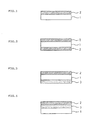
- Figs. 1 through 4 are cross-sectional views demonstrating the stratified structure of conductive substrates in accordance with the present invention.
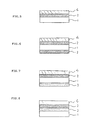
- Figs. 5 through 8 are cross-sectional views demonstrating the stratified structure of recording media in accordance with the present invention.
- Figs. 1 and 2 show the structure of a first and second example of the conductive substrate in accordance with the present invention.
- the conductive substrate is seen consisting of a substrate layer 1 with an overlying first conductive layer 2 which incorporates a copolymer material characteristic of the present invention.
- Fig. 2 shows the second example of a conductive substrate which has two first conductive layers 2, one on either side surface of the intermediate substrate layer 1.
- Fig. 3 shows a third example of a conductive substrate which has a conductive layer 2 similar to that in the conductive substrates shown in Figs.
- an electronic conductive layer 3 is formed consisting of electronic conductive particulate material and binding resin.
- an electronic conductive layer 3 consisting of electronic conductive particulate material and binding resin is formed over one surface of the substrate layer 1 and a conductive layer 2 is formed over the electronic conductive layer 3, the conductive layer 2 being essentially identical to the conductive layer 2 shown in Figs. 1 and 2.
- an image recording layer 4 is applied over the conductive layer 2 of the conductive substrate shown in Fig. 1.
- an image recording layer 4 is applied over one, or optionally both of the first conductive layers 2 of the conductive substrate shown in Fig. 2.
- the image recording layer 4 is formed over the conductive layer 2 of the conductive substrates shown in Figs. 3 and 4, respectively.
- the principle component thereof is an acryl type copolymer formed from polymerizable vinyl monomer of the type shown in chemical structural diagram 1 below in an amount of 10 to 45% by weight, and at least one other type of polymerizable vinyl monomer.
- R1 represents a hydrogen atom or methyl group
- R2 represents an alkylene group
- R3, R4 and R5 represent benzyl groups or one to four carbon atom alkyl groups
- X represents chlorine, bromine, CH3SO4 or C2H5SO4.
- Suitable examples of the polymerizable vinyl monomer shown in chemical structural diagram 1 include quartenary ammonium salts of aminoalkyl (meth)acrylates prepared by reacting dialkylaminoalkyl (meth)acrylates such as dimethylaminoethyl (meth)acrylate, diethylaminoethyl (meth)acrylate, dimethylaminopropyl (meth)acrylate or diethylaminopropyl (meth)acrylate with an alkylating agent such as methyl chloride, ethyl chloride, benzyl chloride, methyl bromide, ethyl bromide, dimethyl sulfate or diethyl sulfate.
- dialkylaminoalkyl (meth)acrylates such as dimethylaminoethyl (meth)acrylate, diethylaminoethyl (meth)acrylate, dimethylaminopropyl (meth)acrylate or diethyla
- suitable examples include, but are not limited to, alkyl (meth)acrylates such as methyl (meth)acrylate, ethyl (meth)acrylate, iso-butyl (meth)acrylate, n-butyl (meth)acrylate, 2-ethylbenzyl (meth)acrylate, methyl (meth)acrylate, hexyl; (meth)acryl amide; acrylonitrile; vinyl acetate; styrene; a-methyl styrene; and vinyl toluene.
- alkyl (meth)acrylates such as methyl (meth)acrylate, ethyl (meth)acrylate, iso-butyl (meth)acrylate, n-butyl (meth)acrylate, 2-ethylbenzyl (meth)acrylate, methyl (meth)acrylate, hexyl; (meth)acryl amide; acrylonitrile; vinyl acetate; s
- first conductive layer 2 is an acryl type copolymer which is formed using conventional copolymerization techniques from polymerizable vinyl monomer of the type shown in chemical structural diagram 1 in an amount of 10 to 45% by weight, and at least one other type of polymerizable vinyl monomer. More preferably, the polymerizable vinyl monomer of the type shown in chemical structural diagram 1 is employed in an amount of 25 to 40% by weight of the acryl type copolymer. If this polymerizable vinyl monomer is used in an amount greater than 45 weight %, the water resistance properties of the resulting conductive substrate and electrostatic recording medium decline to an insufficient level, and printed images and text made therefrom tend to suffer damage when exposed to moisture. On the other hand, if the vinyl monomer is used in an amount less than 10 weight %, the electrical resistance of a conductive substrate becomes too high, resulting in poor recording characteristics such as insufficient darkness or density of printed text.
- conductive materials can be added to the above described first conductive layer 2, wherein the acryl type copolymer functions as a binding resin.
- conductive materials include carbon black, graphite, tin oxide, titanium oxide, zinc oxide, antimony oxide, gold, silver and copper and nickel in powdered form, cationic or anionic high molecular weight electrolyte substances, and conductive whiskers.
- inorganic pigments such as silica, aluminum hydroxide, aluminum oxide, kaolin, talc, mica, calcium carbonate, and organic pigments such as cellulose powder, polyethylene powder, polypropylene powder, as well as acryl type resins, styrene type resins and polyester type resins can be added to the conductive layer 2 of the present invention.
- the surface electrical resistance of the conductive layer 2 should be on the order of from 1 x 10⁵ to 1 x 10⁹ ⁇ .
- conductive whiskers When it is desirable to include conductive whiskers in the conductive layer 2, conductive materials having a crystalline structure and which are in the form of small needles, fibers or the like can be used therefor. Such conductive whiskers can be used in a relatively small amount compared with conventional conduction enhancing materials. Suitable examples of materials for the conductive whiskers include whiskers made of potassium titanate, silicon carbonate, or aluminum borate which has been doped with tin oxide, antimony oxide, gold, silver or the like. Generally, materials for the conductive whiskers should be colorless or white so as to avoid imparting color to recording media incorporating the conductive substrate, for which reason alkali metal titanate (for example potassium titanate) most preferred.
- alkali metal titanate for example potassium titanate
- a length of 0.5 to 100 ⁇ m and a diameter of 0.1 to 1 ⁇ m are preferred in order to provide a homogeneous first conductive layer 2.
- Conductive whiskers having a relatively low longitudinal resistance of 1 x 10⁴ ⁇ cm or less generally provide the best results.
- the optimum proportion is within the range of 15 to 150 parts by weight of conductive whiskers to 100 parts by weight of acryl type copolymer. Because, when used under 15 parts by weight of the whiskers, preferable effect of adding the whiskers cannot be obtained, and when used over 100 parts by weight of the whiskers, resistance of the conductive layer in high humidity becomes unpreferable one. That is, when used outside of the range above, the variation in resistance of the conductive layer 2 with changes in humidity becomes too great, and as a result, printing density tends to be uneven and difficult to control.
- an electronic conductive layer 3 consisting of electronic conductive particulate material and binding resin is included in the third and fourth examples of the conductive substrate and the seventh and eighth examples of the recording media of the present invention.
- suitable examples include carbon black, tin oxide, gold or silver in powdered form; metals oxides such as zinc oxide or indium oxide which have been doped with antimony oxide or tin oxide; and conductive whiskers consisting of fine needles of potassium titanate, silicon carbide, aluminum borate and the like doped with antimony oxide or tin oxide.
- Suitable materials for the binding resin include polyesters, polycarbonates, polyamide, polyurethane, (meth)acrylate resins, styrene resins, butyral resins, fluorocarbon resins and the like.
- the surface electrical resistance of the conductive layer 2 should be on the order of from 1 x 10⁵ to 1 x 10⁹ ⁇ .
- suitable materials include, but are not limited to, paper, synthetic paper, fabrics, unwoven cloth, numerous types of resin film and animal skins.
- the substrate layer 1 should preferably be made from resin film, fabrics, or from paper which has been coated or impregnated with synthetic resin.
- a conductive layer 2 or 3 is applied over at least one of the surfaces of the substrate layer 1.
- an image recording layer 4 is applied over one or both of the surface of the conductive layer 2 of the conductive substrate.
- Suitable materials for the image recording layer in the case of electrostatic recording media include various types of organic solvent soluble high resistance resin compounds which function as a dielectric layer, for example, polyester, polycarbonate, polyamide, polyurethane, (meth)acrylate resins, styrene resins, butyral resins, olefin resins, silicon resin, fluorocarbon resins.
- the image recording layer should include a material which is photoconductive such as zinc oxide, dispersed in binding resin.
- the components making up conductive layers 2 and 3 of the present invention can be dissolved and/or dispersed in a solvent such as water, methanol, ethanol, toluene, acetone, methylethyl ketone or ethyl acetate, the applied over the underlying layer by a technique such as air-knife coating, roll coating, wire-bar coating, spray coating, fountain coating, reverse-roll coating and the like, followed by drying.
- a solvent such as water, methanol, ethanol, toluene, acetone, methylethyl ketone or ethyl acetate
- a barrier layer can be applied over one or both surfaces of the substrate layer before applying any subsequent layers.
- Suitable constituents thereof include, but are not limited to, various resin emulsions such as styrene-butadiene copolymer resin, acrylate-acrylic acid copolymer, styren-acryl copolymer, vinyl acetate-acryl copolymer, vinyl chloride, vinyl chloride-vinylacetate copolymer.
- organic or inorganic pigments can be incorporated in such a barrier layer when desired.
- a conductive layer was applied over one surface thereof at 5 g/m2 as a solution prepared by dissolving 30 parts of an acryl type copolymer in 70 parts of a 50/50 mixture of methanol/methylethyl ketone, the acryl type copolymer consisting of 40 parts by weight of the quartenary ammonium salt: 30 parts by weight of methyl methacrylate and 30 parts by weight of n-butyl methacrylate.
- the procedure of the first example was repeated, except that the acryl the copolymer consisted of 30 parts by weight of the quartenary ammonium salt, 35 parts by weight of methyl methacrylate and 35 parts by weight of n-butyl methacrylate.
- Example 7 20 parts of the acryl type copolymer consisting of 40 parts by weight of the quartenary ammonium salt: 30 parts by weight of methyl methacrylate and 30 parts by weight of n-butyl methacrylate, blended with 10 parts of calcium carbonate was dispersed in 70 parts of a 50/50 mixture of methanol/methylethyl ketone. The resulting suspension was then applied over a paper substrate layer identical to that of Example 1, in an amount of 7 g/m2.
- Example 8 the procedure of the Example 1 was repeated, except that the acryl type copolymer consisted of 10 parts by weight of the quartenary ammonium salt, 45 parts by weight of methyl methacrylate and 45 parts by weight of n-butyl methacrylate.
- Example 9 20 parts of the acryl type copolymer consisting of 10 parts by weight of the quartenary ammonium salt:
- Example 10 using 50 g/m2 high quality paper as the substrate layer, a conductive layer was applied over one surface thereof at 5 g/m2 as a dispersion prepared by mixing 21 parts of an acryl type copolymer and 9 parts of conductive potassium titanate whiskers (Otsuka Chemical Industries, Dentall WK-300) with 70 parts of a 50/50 mixture of methanol/methylethyl ketone, then dried, the acryl type copolymer consisting of 40 parts by weight of the quartenary ammonium salt: 30 parts by weight of methyl methacrylate and 30 parts by weight of n-butyl methacrylate.
- a conductive layer was applied over one surface thereof at 5 g/m2 as a dispersion prepared by mixing 21 parts of an acryl type copolymer and 9 parts of conductive potassium titanate whiskers (Otsuka Chemical Industries, Dentall WK-300) with 70 parts of a 50/50 mixture of methanol/methylethyl ketone,
- Example 11 the procedure of Example 10 was repeated, except that the acryl type copolymer consisted of 30 parts by weight of the quartenary ammonium salt: 35 parts by weight of methyl methacrylate and 35 parts by weight of n-butyl methacrylate.
- Example 12 the procedure of Example 10 was repeated, except that the quartenary ammonium salt of the acryl type copolymer was replaced with one of the following four quartenary ammonium salts:
- Example 16 a conductive layer was applied over one surface of a paper substrate layer identical to that of Example 10 at 8 g/m2 as a dispersion prepared by mixing 25 parts of an acryl type copolymer and 5 parts of conductive potassium titanate whiskers (Otsuka Chemical Industries, Dentall WK-300) with 70 parts of a 50/50 mixture of methanol/methylethyl ketone, then dried, the acryl type copolymer consisting of 40 parts by weight of the quartenary ammonium salt: 30 parts by weight of methyl methacrylate and 30 parts by weight of n-butyl methacrylate.
- Example 17 a conductive layer was applied over one surface of a paper substrate layer identical to that of Example 10 at 6 g/m2 as a dispersion prepared by mixing 12 parts of an acryl type copolymer and 18 parts of conductive potassium titanate whiskers (Otsuka Chemical Industries, Dentall WK-300) with 70 parts of a 50/50 mixture of methanol/methylethyl ketone, then dried, the acryl type copolymer consisting of 10 parts by weight of the quartenary ammonium salt: 45 parts by weight of methyl methacrylate and 45 parts by weight of n-butyl methacrylate.
- Example 1 Using the conductive substrate prepared in Example 1 (as shown in Fig. 1), the uncoated surface of the substrate layer thereof was coated with 5 g/m2 of a dispersion consisting of 50 parts of conductive potassium titanate whiskers (Otsuka Chemical Industries, Dentall WK-300), 125 parts of polyester resin (Toyo Textiles, Vyron 240) and 75 parts of methylethyl ketone (Fig. 3).
- conductive potassium titanate whiskers Olephthalate whiskers
- polyester resin Toyo Textiles, Vyron 240
- Fig. 3 75 parts of methylethyl ketone
- Example 18 The procedure of Example 18 was repeated, except the uncoated surface of the substrate layer was coated with 5 g/m2 of a dispersion consisting of 70 parts of conductive zinc oxide (HakuSui Chemical Corporation, 23-K), 75 parts of polyester resin (Toyo Textiles, Vyron 240), 55 parts of toluene and 50 parts of methylethyl ketone.
- a dispersion consisting of 70 parts of conductive zinc oxide (HakuSui Chemical Corporation, 23-K), 75 parts of polyester resin (Toyo Textiles, Vyron 240), 55 parts of toluene and 50 parts of methylethyl ketone.
- Example 2 Using the conductive substrate prepared in Example 1 (as shown in Fig. 1), the conductive layer applied in that example was then covered with the electronic conductive layer at 5 g/m2, consisting of a dispersion consisting of 50 parts of conductive potassium titanate whiskers (Otsuka Chemical Industries, Dentall WK-300), 125 parts of polyester resin (Toyo Textiles, Vyron 240) and 75 parts of methylethyl ketone (Fig. 4).
- conductive potassium titanate whiskers Olephthalate whiskers
- polyester resin Toyo Textiles, Vyron 240
- Fig. 4 75 parts of methylethyl ketone
- Example 1 The procedure of Example 1 was repeated, except that the acryl type copolymer consisted of 5 parts of the quartenary ammonium salt, 50 parts of methyl methacrylate and 45 parts of n-butyl methacrylate.
- Example 1 The procedure of Example 1 was repeated, except that the acryl type copolymer consisted of 50 parts of the quartenary ammonium salt, 25 parts of methyl methacrylate and 25 parts of n-butyl methacrylate.
- Example 17 The procedure of Example 17 was repeated, except that the dispersion applied consisted of 20 parts of the acryl type copolymer and 10 parts of calcium carbonate with 70 parts of a 50/50 mixture of methanol/methylethyl ketone, the acryl type copolymer consisting of 5 parts by weight of the quartenary ammonium salt: 50 parts by weight of methyl methacrylate and 45 parts by weight of n-butyl methacrylate.
- Example 10 The procedure of Example 10 was repeated, except that the dispersion prepared consisted of 21 parts of copolymer and 9 parts of conductive potassium titanate whiskers (Otsuka Chemical Industries, Dentall WK-300) with 70 parts of a 50/50 mixture of methanol/methylethyl ketone, the acryl type copolymer consisting of 50 parts by weight of methyl methacrylate and 50 parts by weight of n-butyl methacrylate.
- conductive potassium titanate whiskers Olethyl ketone
- Example 2 The procedure of Example 1 was repeated, except that the applied layer consisted entirely of the following quartenary ammonium salt:
- a layer of the below Composition A was applied over one surface at 5 g/m2 and dried, and a layer of the below Composition B was applied over the other surface at 5 g/m2.
- Example 20 The procedure of Example 20 was repeated, except that the acryl type copolymer layer was replaced with a layer of the above Composition B.
- the electrostatic recording media in accordance with the present invention demonstrated remarkable printing quality and resistance to water damage.
- flat flat plate printing blanks were prepared by applying a 15 ⁇ m thick photosensitive layer to each consisting of: Thus prepared, the flat plate printing blanks were tested for water resistance by immersion in water for 24 hours. Again, the media in accordance with the present invention was found to demonstrate excellent resistance to water damage. Additionally, flat plate printing blanks prepared from each sample were then utilized in a flat plate printing process under the conditions listed below, each developed and etched blank used to continuously print 5000 sheets.
Landscapes
- Physics & Mathematics (AREA)
- Spectroscopy & Molecular Physics (AREA)
- General Physics & Mathematics (AREA)
- Chemical & Material Sciences (AREA)
- Inorganic Chemistry (AREA)
- Photoreceptors In Electrophotography (AREA)
Applications Claiming Priority (6)
| Application Number | Priority Date | Filing Date | Title |
|---|---|---|---|
| JP124155/90 | 1990-05-16 | ||
| JP12415590 | 1990-05-16 | ||
| JP210468/90 | 1990-08-10 | ||
| JP21046890A JPH0497156A (ja) | 1990-08-10 | 1990-08-10 | 導電性支持体及びそれを使用した静電記録体 |
| JP415241/90 | 1990-12-27 | ||
| JP41524190A JPH04134352A (ja) | 1990-05-16 | 1990-12-27 | 導電性支持体及びそれを使用した記録体 |
Publications (2)
| Publication Number | Publication Date |
|---|---|
| EP0459918A1 true EP0459918A1 (de) | 1991-12-04 |
| EP0459918B1 EP0459918B1 (de) | 1995-12-06 |
Family
ID=27314872
Family Applications (1)
| Application Number | Title | Priority Date | Filing Date |
|---|---|---|---|
| EP91420158A Expired - Lifetime EP0459918B1 (de) | 1990-05-16 | 1991-05-16 | Leitfähiges Substrat und seine Verwendung in den Druckmedien |
Country Status (3)
| Country | Link |
|---|---|
| US (1) | US5234746A (de) |
| EP (1) | EP0459918B1 (de) |
| DE (1) | DE69115126T2 (de) |
Cited By (2)
| Publication number | Priority date | Publication date | Assignee | Title |
|---|---|---|---|---|
| EP0587508A3 (de) * | 1992-08-28 | 1994-11-09 | Tomoegawa Paper Co Ltd | Elektrostatisches Aufzeichnungsmedium. |
| US6656935B2 (en) | 1999-09-16 | 2003-12-02 | Tanabe Seiyaku Co., Ltd. | Aromatic nitrogen-containing 6-membered cyclic compounds |
Families Citing this family (2)
| Publication number | Priority date | Publication date | Assignee | Title |
|---|---|---|---|---|
| JPH0746235B2 (ja) * | 1990-06-04 | 1995-05-17 | 株式会社巴川製紙所 | 導電性支持体 |
| EP2015939B1 (de) * | 2006-04-03 | 2011-09-07 | Arkwright Advanced Coating, Inc. | Tintenstrahlbedruckbares transferpapier mit kationischer schicht unter der bildschicht |
Citations (5)
| Publication number | Priority date | Publication date | Assignee | Title |
|---|---|---|---|---|
| FR2029625A1 (de) * | 1969-01-29 | 1970-10-23 | Agfa Gevaert Nv | |
| FR2079010A5 (de) * | 1970-02-25 | 1971-11-05 | Ici Ltd | |
| FR2239557A1 (en) * | 1973-08-01 | 1975-02-28 | Ici Ltd | Quat ammonium -contg (co)polymer compsn - used as coating for prodn of paper for electrographic printing |
| DE2551018A1 (de) * | 1974-11-16 | 1976-08-12 | Konishiroku Photo Ind | Lichtempfindliche elektrophotographische platte |
| EP0011486A1 (de) * | 1978-11-15 | 1980-05-28 | Calgon Corporation | Elektroleitfähige Kunstharzbeschichtungen für Aufzeichnungspapier mit verbesserter Lösungsmittelbeständigkeit sowie damit beschichtetes Papier |
Family Cites Families (4)
| Publication number | Priority date | Publication date | Assignee | Title |
|---|---|---|---|---|
| JPS6126435A (ja) * | 1984-07-13 | 1986-02-05 | 九州日立マクセル株式会社 | 充電回路 |
| JPS62131265A (ja) * | 1985-12-03 | 1987-06-13 | Ricoh Co Ltd | 透明静電記録体 |
| JPS63318568A (ja) * | 1987-06-22 | 1988-12-27 | Tomoegawa Paper Co Ltd | 導電性支持体 |
| JP2605789B2 (ja) * | 1988-03-30 | 1997-04-30 | 松下電器産業株式会社 | 電子写真感光体 |
-
1991
- 1991-05-16 EP EP91420158A patent/EP0459918B1/de not_active Expired - Lifetime
- 1991-05-16 DE DE69115126T patent/DE69115126T2/de not_active Expired - Fee Related
- 1991-05-16 US US07/700,809 patent/US5234746A/en not_active Expired - Lifetime
Patent Citations (5)
| Publication number | Priority date | Publication date | Assignee | Title |
|---|---|---|---|---|
| FR2029625A1 (de) * | 1969-01-29 | 1970-10-23 | Agfa Gevaert Nv | |
| FR2079010A5 (de) * | 1970-02-25 | 1971-11-05 | Ici Ltd | |
| FR2239557A1 (en) * | 1973-08-01 | 1975-02-28 | Ici Ltd | Quat ammonium -contg (co)polymer compsn - used as coating for prodn of paper for electrographic printing |
| DE2551018A1 (de) * | 1974-11-16 | 1976-08-12 | Konishiroku Photo Ind | Lichtempfindliche elektrophotographische platte |
| EP0011486A1 (de) * | 1978-11-15 | 1980-05-28 | Calgon Corporation | Elektroleitfähige Kunstharzbeschichtungen für Aufzeichnungspapier mit verbesserter Lösungsmittelbeständigkeit sowie damit beschichtetes Papier |
Non-Patent Citations (5)
| Title |
|---|
| PATENT ABSTRACTS OF JAPAN vol. 11, no. 354 (P-638)(2801) 19 November 1987; & JP-A-62 131 265 (RICOH CO LTD) 13 June 1987 * |
| PATENT ABSTRACTS OF JAPAN vol. 12, no. 458 (P-794)(3305) 02 December 1988; & JP-A-63 180 964 (RICOH CO LTD) 26 July 1988, * |
| PATENT ABSTRACTS OF JAPAN vol. 13, no. 162 (P-859)(3510) 19 April 1989; & JP-A-63 318 568 (TOMOEGAWA PAPER CO LTD) 27 December 1988 * |
| PATENT ABSTRACTS OF JAPAN vol. 13, no. 586 (P-982)(3934) 25 December 1989; & JP-A-1 248 158 (MATSUSHITA ELECTRIC IND CO LTD) 03 October 1989 * |
| RESEARCH DISCLOSURE. vol. 2244, no. 164, December 1977, HAVANT GB, pages 72 - 73; "crosslinkable conductive polymers" * |
Cited By (2)
| Publication number | Priority date | Publication date | Assignee | Title |
|---|---|---|---|---|
| EP0587508A3 (de) * | 1992-08-28 | 1994-11-09 | Tomoegawa Paper Co Ltd | Elektrostatisches Aufzeichnungsmedium. |
| US6656935B2 (en) | 1999-09-16 | 2003-12-02 | Tanabe Seiyaku Co., Ltd. | Aromatic nitrogen-containing 6-membered cyclic compounds |
Also Published As
| Publication number | Publication date |
|---|---|
| DE69115126D1 (de) | 1996-01-18 |
| US5234746A (en) | 1993-08-10 |
| EP0459918B1 (de) | 1995-12-06 |
| DE69115126T2 (de) | 1996-05-09 |
Similar Documents
| Publication | Publication Date | Title |
|---|---|---|
| CA2116734C (en) | Imaging element comprising an electrically-conductive layer containing water-insoluble polymer particles | |
| US4456670A (en) | Photosensitive material for lithographic printing | |
| JPS5942864B2 (ja) | 投影用原稿の作成方法及びそれに用いる静電写真用転写フイルム | |
| JPH0675417A (ja) | 電子写真印刷用媒体 | |
| US4168338A (en) | Transfer sheet with toner-receiving layer of thermoplastic and thermosetting polymers | |
| EP0877298A2 (de) | Beschichtetes xerographisches photographisches Papier | |
| US4081583A (en) | Electrostatic recording material | |
| US3639640A (en) | Electrostatographic recording element | |
| US4245025A (en) | Transfer sheet and process for preparation thereof | |
| US4268595A (en) | Electrostatic recording material and method for the production thereof | |
| EP0459918B1 (de) | Leitfähiges Substrat und seine Verwendung in den Druckmedien | |
| CA1104858A (en) | Plate for lithography or offset printing with oleophilic iron oxide areas and hydrophilic etched inorganic pigment areas | |
| CA2032840C (en) | Conductive coating compositions | |
| US4241134A (en) | Electrostatically imageable drafting film | |
| US5480752A (en) | Electrophotographic lithograph printing plate material | |
| EP0104082B1 (de) | Elektrophotographische Offset-Druckform | |
| EP0699314A1 (de) | Elektrostatische aufzeichnungsmedien | |
| US3950595A (en) | Transferring paper for electrophotography | |
| CA2139932A1 (en) | Nonimpact printing element | |
| JPH04134352A (ja) | 導電性支持体及びそれを使用した記録体 | |
| EP0270032B1 (de) | Elektrostatische Aufzeichnungsmethode | |
| JPH0531135B2 (de) | ||
| EP0587508B1 (de) | Elektrostatisches Aufzeichnungsmedium | |
| DE3222134A1 (de) | Lichtempfindliches element fuer elektrofotografische zwecke | |
| JPS59121343A (ja) | 電子写真用導電性基紙 |
Legal Events
| Date | Code | Title | Description |
|---|---|---|---|
| PUAI | Public reference made under article 153(3) epc to a published international application that has entered the european phase |
Free format text: ORIGINAL CODE: 0009012 |
|
| AK | Designated contracting states |
Kind code of ref document: A1 Designated state(s): DE FR GB |
|
| RIN1 | Information on inventor provided before grant (corrected) |
Inventor name: KAMIMURA, KENO, C/O TOMOEGAWA PAPER CO., LTD. Inventor name: OKI, TOMIO, C/O TOMOEGAWA PAPER CO., LTD. Inventor name: IWAMOTO, KIYOSHI, C/O TOMOEGAWA PAPER CO., LTD. |
|
| 17P | Request for examination filed |
Effective date: 19920325 |
|
| 17Q | First examination report despatched |
Effective date: 19930120 |
|
| GRAA | (expected) grant |
Free format text: ORIGINAL CODE: 0009210 |
|
| AK | Designated contracting states |
Kind code of ref document: B1 Designated state(s): DE FR GB |
|
| ET | Fr: translation filed | ||
| REF | Corresponds to: |
Ref document number: 69115126 Country of ref document: DE Date of ref document: 19960118 |
|
| PLBE | No opposition filed within time limit |
Free format text: ORIGINAL CODE: 0009261 |
|
| STAA | Information on the status of an ep patent application or granted ep patent |
Free format text: STATUS: NO OPPOSITION FILED WITHIN TIME LIMIT |
|
| 26N | No opposition filed | ||
| REG | Reference to a national code |
Ref country code: GB Ref legal event code: IF02 |
|
| PGFP | Annual fee paid to national office [announced via postgrant information from national office to epo] |
Ref country code: GB Payment date: 20050503 Year of fee payment: 15 |
|
| PGFP | Annual fee paid to national office [announced via postgrant information from national office to epo] |
Ref country code: DE Payment date: 20050510 Year of fee payment: 15 |
|
| PGFP | Annual fee paid to national office [announced via postgrant information from national office to epo] |
Ref country code: FR Payment date: 20050531 Year of fee payment: 15 |
|
| PG25 | Lapsed in a contracting state [announced via postgrant information from national office to epo] |
Ref country code: GB Free format text: LAPSE BECAUSE OF NON-PAYMENT OF DUE FEES Effective date: 20060516 |
|
| PG25 | Lapsed in a contracting state [announced via postgrant information from national office to epo] |
Ref country code: DE Free format text: LAPSE BECAUSE OF NON-PAYMENT OF DUE FEES Effective date: 20061201 |
|
| GBPC | Gb: european patent ceased through non-payment of renewal fee |
Effective date: 20060516 |
|
| REG | Reference to a national code |
Ref country code: FR Ref legal event code: ST Effective date: 20070131 |
|
| PG25 | Lapsed in a contracting state [announced via postgrant information from national office to epo] |
Ref country code: FR Free format text: LAPSE BECAUSE OF NON-PAYMENT OF DUE FEES Effective date: 20060531 |