EP0460285B1 - Procédé de fabrication d'un transistor bipolaire ayant une capacité base-collecteur extrêmement réduite - Google Patents
Procédé de fabrication d'un transistor bipolaire ayant une capacité base-collecteur extrêmement réduite Download PDFInfo
- Publication number
- EP0460285B1 EP0460285B1 EP90123356A EP90123356A EP0460285B1 EP 0460285 B1 EP0460285 B1 EP 0460285B1 EP 90123356 A EP90123356 A EP 90123356A EP 90123356 A EP90123356 A EP 90123356A EP 0460285 B1 EP0460285 B1 EP 0460285B1
- Authority
- EP
- European Patent Office
- Prior art keywords
- collector
- layer
- emitter
- base
- sub
- Prior art date
- Legal status (The legal status is an assumption and is not a legal conclusion. Google has not performed a legal analysis and makes no representation as to the accuracy of the status listed.)
- Expired - Lifetime
Links
Images

Classifications
-
- H—ELECTRICITY
- H10—SEMICONDUCTOR DEVICES; ELECTRIC SOLID-STATE DEVICES NOT OTHERWISE PROVIDED FOR
- H10D—INORGANIC ELECTRIC SEMICONDUCTOR DEVICES
- H10D10/00—Bipolar junction transistors [BJT]
- H10D10/01—Manufacture or treatment
- H10D10/021—Manufacture or treatment of heterojunction BJTs [HBT]
-
- H—ELECTRICITY
- H10—SEMICONDUCTOR DEVICES; ELECTRIC SOLID-STATE DEVICES NOT OTHERWISE PROVIDED FOR
- H10D—INORGANIC ELECTRIC SEMICONDUCTOR DEVICES
- H10D62/00—Semiconductor bodies, or regions thereof, of devices having potential barriers
- H10D62/10—Shapes, relative sizes or dispositions of the regions of the semiconductor bodies; Shapes of the semiconductor bodies
- H10D62/113—Isolations within a component, i.e. internal isolations
- H10D62/115—Dielectric isolations, e.g. air gaps
-
- H—ELECTRICITY
- H10—SEMICONDUCTOR DEVICES; ELECTRIC SOLID-STATE DEVICES NOT OTHERWISE PROVIDED FOR
- H10D—INORGANIC ELECTRIC SEMICONDUCTOR DEVICES
- H10D62/00—Semiconductor bodies, or regions thereof, of devices having potential barriers
- H10D62/80—Semiconductor bodies, or regions thereof, of devices having potential barriers characterised by the materials
- H10D62/85—Semiconductor bodies, or regions thereof, of devices having potential barriers characterised by the materials being Group III-V materials, e.g. GaAs
-
- Y—GENERAL TAGGING OF NEW TECHNOLOGICAL DEVELOPMENTS; GENERAL TAGGING OF CROSS-SECTIONAL TECHNOLOGIES SPANNING OVER SEVERAL SECTIONS OF THE IPC; TECHNICAL SUBJECTS COVERED BY FORMER USPC CROSS-REFERENCE ART COLLECTIONS [XRACs] AND DIGESTS
- Y10—TECHNICAL SUBJECTS COVERED BY FORMER USPC
- Y10S—TECHNICAL SUBJECTS COVERED BY FORMER USPC CROSS-REFERENCE ART COLLECTIONS [XRACs] AND DIGESTS
- Y10S148/00—Metal treatment
- Y10S148/01—Bipolar transistors-ion implantation
Definitions
- the present invention relates to a method for producing bipolar transistors according to the preamble of claim 1.
- the transit frequency and the maximum oscillation frequency are strongly influenced by parasitic capacitances and series resistances.
- parasitic capacitances are the capacitance between the emitter layer and the base layer or between the base layer and the collector layer outside the inner transistor region.
- the path resistance of the base and the base-collector capacitance must be minimized.
- the object of the present invention is to provide an easy to carry out manufacturing process for bipolar transistors, the characteristics of which are not deteriorated compared to bipolar transistors produced by conventional methods and which have a minimal base-collector capacitance.
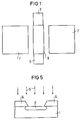
- Fig. 1 shows a plan view of the finished transistor with the arrangement of the contacts for the base, the emitter and the collector.
- FIG. 5 shows the method step corresponding to FIG. 2 in an alternative embodiment.
- the manufacturing method according to the invention circumvents the subsequent insulation implantation by forming a subcollector region locally limited to the inner transistor by lateral insulation implantation before the actual transistor layers are grown.
- the base contact 7, the emitter contact 8 and the collector contact 9 are shown in supervision.
- the area occupied by the sub-collector produced according to the invention comprises the areas occupied by the emitter contact 8 and by the collector contact 9.
- a sub-collector layer 2 which is highly doped for good conductivity, is deposited on a substrate 1.
- the substrate 1 is made of insulating semiconductor material and is advantageously provided with alignment marks.
- the one for the sub-collector The intended area is covered with a first mask 10 (see FIG. 2).
- This covered area of the subcollector has only the size of the inner transistor (ie essentially the emitter area) plus a lateral lead-out for the later collector connection by means of a contact on the subcollector 12.
- the remaining portion of the subcollector layer 2 is covered by an insulation implantation 15 (e.g. . Oxygen) isolated, or at least this insulation implantation 15 greatly reduces the electrical conductivity of this portion of the sub-collector layer 2.
- FIGS. 3 and 4 show the subcollector 12 and the insulating regions 11 which laterally delimit the subcollector 12 and are treated by the insulation implantation 15.
- the emitter is adjusted to the subcollector 12 by an etching step using the second mask 13, in which the material of the cover layer 6 and the emitter layer 5 is removed from the side of this second mask 13, or by a lateral insulation implantation in which the emitter region passes through them second mask 13 is covered.
- a part of the cover layer 6 and the emitter layer 5 is then etched away in a later method step.
- a particular advantage of the method according to the invention is that the collector layer 3 is depleted of charge carriers in the regions above the insulating regions 11 of the sub-collector layer 2 and therefore does not make any contribution to the base collector capacity. Is the sub-collector layer 2 completely insulated under the base connection, i. H. If the base contacts 7 are in the vertical projection above the insulating regions 11 and isolate these regions 11 completely, then the extrinsic “parasitic” base-collector capacitance is practically zero.
- the first mask 14 is applied directly to the substrate 1 from e.g. B. GaAs applied.
- This first mask 14 leaves the area provided for the sub-collector free, that is to say it covers just that part of the substrate surface which is complementary to the first exemplary embodiment.
- An implantation 16 for doping is then carried out by opening this first mask 14, as a result of which the initially semi-insulating substrate 1 becomes conductive in the area provided for the sub-collector 12.
- the first mask 14 is then removed, the surface of the substrate is cleaned and the doping is healed.
- the same method steps as in the first exemplary embodiment then take place, i. H. the growth of the layers according to FIG. 3. The remaining method steps correspond to the first embodiment.
- the extrinsic base-collector capacitance can be reduced by a factor of about 2, that is, by the isolation implantation with oxygen corresponding to the state of the art through the finished layer sequence of the transistor then only half of the base-collector capacity is due to the contribution from the extrinsic base-collector capacity. As a result, the collector charging time and the emitter charging time are reduced significantly.
- the method according to the invention not only allows the implantation implantation to be carried out simply, but also enables the extrinsic base-collector capacitance to be virtually completely eliminated, ie the base-collector capacitance is reduced to one third compared to conventional transistors. Avoiding the parasitic extrinsic base-collector capacitance offers further advantages:
- the connection areas for the base contacts 7 can be chosen larger if, for. B. lower base contact resistances z. B. to increase the maximum oscillation frequency because the extrinsic base-collector capacitance no longer needs to be taken into account.
- the method according to the invention can be used in all material systems in which further layers, ie. H. the collector layer (3), the base layer (4) and the emitter layer (5) are grown.
- Such material systems are e.g. B. GaAs / GaAlAs, InP / InGaAs and Si / SiGe.
Landscapes
- Bipolar Transistors (AREA)
Claims (7)
- Procédé de fabrication d'un transistor bipolaire porté par un substrat (1) en matériau semi-conducteur, dans lequel on dépose les unes au-dessus des autres une couche de collecteur (3), une couche de base (4) et une couche d'émetteur (5) pour la formation d'un collecteur, d'une base et d'un émetteur,
caractérisé
en ce qu'avant le dépôt de la couche de collecteur (3), de la couche de base (4) et de la couche d'émetteur (5), on forme un sous-collecteur (12) qui est limité à la région prévue pour l'émetteur et pour une connexion du collecteur. - Procédé selon la revendication 1,
caractériséen ce qu'on dépose une couche de sous-collecteur (2) sur le substrat (1),en ce que, en utilisant un premier masque (10) qui recouvre la région prévue pour le sous-collecteur (12), on procède à une implantation d'isolant (15) eten ce qu'après avoir enlevé ce premier masque (10) et après avoir déposé la couche de collecteur (3), la couche de base (4) et la couche d'émetteur (5), on forme l'émetteur de manière alignée sur le sous-collecteur (12) en utilisant un deuxième masque (13). - Procédé selon la revendication 1,
caractériséen ce qu'on implante un dopage dans le substrat (1) en utilisant un premier masque (14) qui laisse libre la région prévue pour le sous-collecteur (12), eten ce qu'après avoir enlevé ce premier masque (14) et après avoir déposé la couche de collecteur (3), la couche de base (4) et la couche d'émetteur (5), on forme l'émetteur de manière alignée sur le sous-collecteur (12) en utilisant un deuxième masque (13). - Procédé selon l'une des revendications 1 à 3,
caractériséen ce que le substrat (1) est un GaAs semi-isolant et,en ce que, pour la couche de collecteur (3), la couche de base (4) et la couche d'émetteur (5), on dépose des matériaux semi-conducteurs pris dans le système GaAs/GaAlAs. - Procédé selon l'une des revendications 1 à 3,
caractériséen ce que le substrat (1) est un InP semi-isolant eten ce que, pour la couche de collecteur (3), la couche de base (4) et la couche d'émetteur (5), on dépose par épitaxie des matériaux semi-conducteurs pris dans le système InP/InGaAs. - Procédé selon l'une des revendications 1 à 3,
caractériséen ce que le substrat (1) est fait de Si semi-isolant eten ce que, pour la couche de collecteur (3), la couche de base (4) et la couche d'émetteur (5), on dépose par épitaxie des matériaux semi-conducteurs pris dans le système Si/SiGe. - Procédé selon l'une des revendications 1 à 6,
caractérisé
en ce que le sous-collecteur (12), la couche de collecteur (3) et la couche d'émetteur (4) sont dopées pour posséder une conductivité N.
Applications Claiming Priority (2)
| Application Number | Priority Date | Filing Date | Title |
|---|---|---|---|
| DE4018298 | 1990-06-07 | ||
| DE4018298 | 1990-06-07 |
Publications (3)
| Publication Number | Publication Date |
|---|---|
| EP0460285A2 EP0460285A2 (fr) | 1991-12-11 |
| EP0460285A3 EP0460285A3 (fr) | 1992-12-30 |
| EP0460285B1 true EP0460285B1 (fr) | 1996-08-28 |
Family
ID=6407991
Family Applications (1)
| Application Number | Title | Priority Date | Filing Date |
|---|---|---|---|
| EP90123356A Expired - Lifetime EP0460285B1 (fr) | 1990-06-07 | 1990-12-05 | Procédé de fabrication d'un transistor bipolaire ayant une capacité base-collecteur extrêmement réduite |
Country Status (4)
| Country | Link |
|---|---|
| US (1) | US5070028A (fr) |
| EP (1) | EP0460285B1 (fr) |
| JP (1) | JPH0513427A (fr) |
| DE (1) | DE59010471D1 (fr) |
Families Citing this family (6)
| Publication number | Priority date | Publication date | Assignee | Title |
|---|---|---|---|---|
| US5298438A (en) * | 1992-08-31 | 1994-03-29 | Texas Instruments Incorporated | Method of reducing extrinsic base-collector capacitance in bipolar transistors |
| DE19533677A1 (de) * | 1995-09-12 | 1997-03-13 | Daimler Benz Ag | Verfahren zur Herstellung eines Heterobipolartransistors |
| US5672522A (en) * | 1996-03-05 | 1997-09-30 | Trw Inc. | Method for making selective subcollector heterojunction bipolar transistors |
| US5625206A (en) * | 1996-06-03 | 1997-04-29 | Lucent Technologies Inc. | High-speed double-heterostructure bipolar transistor devices |
| FR2778022B1 (fr) * | 1998-04-22 | 2001-07-13 | France Telecom | Transistor bibolaire vertical, en particulier a base a heterojonction sige, et procede de fabrication |
| US8975146B2 (en) | 2013-05-01 | 2015-03-10 | International Business Machines Corporation | Trench isolation structures and methods for bipolar junction transistors |
Family Cites Families (12)
| Publication number | Priority date | Publication date | Assignee | Title |
|---|---|---|---|---|
| US3687722A (en) * | 1971-03-10 | 1972-08-29 | Rca Corp | Method of coating selective areas of the surface of a body |
| US4380774A (en) * | 1980-12-19 | 1983-04-19 | The United States Of America As Represented By The Secretary Of The Navy | High-performance bipolar microwave transistor |
| JPS57126131A (en) * | 1981-01-28 | 1982-08-05 | Toshiba Corp | Manufacture of semiconductor device |
| US4728616A (en) * | 1982-09-17 | 1988-03-01 | Cornell Research Foundation, Inc. | Ballistic heterojunction bipolar transistor |
| JPS60253267A (ja) * | 1984-05-29 | 1985-12-13 | Toshiba Corp | ヘテロ接合バイポ−ラトランジスタおよびその製造方法 |
| CA1252227A (fr) * | 1984-07-09 | 1989-04-04 | Fairchild Camera And Instrument Corporation | Contact de base en siliciure auto-aligne pour transistor bipolaire |
| US4663831A (en) * | 1985-10-08 | 1987-05-12 | Motorola, Inc. | Method of forming transistors with poly-sidewall contacts utilizing deposition of polycrystalline and insulating layers combined with selective etching and oxidation of said layers |
| US4682407A (en) * | 1986-01-21 | 1987-07-28 | Motorola, Inc. | Means and method for stabilizing polycrystalline semiconductor layers |
| JPS63179547A (ja) * | 1987-01-21 | 1988-07-23 | Mitsubishi Electric Corp | 導電性薄膜の加工方法 |
| GB8708926D0 (en) * | 1987-04-14 | 1987-05-20 | British Telecomm | Bipolar transistor |
| US4839303A (en) * | 1987-10-13 | 1989-06-13 | Northrop Corporation | Planar bipolar transistors including heterojunction transistors and method |
| JPH0241867A (ja) * | 1988-07-28 | 1990-02-13 | Yasushi Kato | 球研磨装置 |
-
1990
- 1990-12-05 DE DE59010471T patent/DE59010471D1/de not_active Expired - Fee Related
- 1990-12-05 EP EP90123356A patent/EP0460285B1/fr not_active Expired - Lifetime
-
1991
- 1991-04-01 US US07/678,047 patent/US5070028A/en not_active Expired - Fee Related
- 1991-06-05 JP JP3162198A patent/JPH0513427A/ja active Pending
Also Published As
| Publication number | Publication date |
|---|---|
| DE59010471D1 (de) | 1996-10-02 |
| EP0460285A2 (fr) | 1991-12-11 |
| US5070028A (en) | 1991-12-03 |
| JPH0513427A (ja) | 1993-01-22 |
| EP0460285A3 (fr) | 1992-12-30 |
Similar Documents
| Publication | Publication Date | Title |
|---|---|---|
| DE69605718T2 (de) | Völlig selbstjustierter Submikrometer-Bipolartransistor mit einem Heteroübergang und Verfahren zu dessen Herstellung | |
| DE69328758T2 (de) | Verfahren zur Herstellung von SOI-Bipolar- und MOS-Transistoren | |
| DE4445345C2 (de) | Verfahren zur Herstellung eines Bipolartransistors | |
| DE1764464C3 (de) | Verfahren zur Herstellung eines lateralen Transistors | |
| DE69524516T2 (de) | Verfahren zur Herstellung eines Bipolatransistors | |
| DE4015067C2 (de) | Transistor mit permeabler Basis | |
| DE3850309T2 (de) | Hochfrequenz-Bipolartransistor und dessen Herstellungsverfahren. | |
| DE4014216C2 (de) | Verfahren zum Herstellen eines Hetero-Bipolar-Transistors | |
| EP0687013B1 (fr) | Transistor bipolaire et procédé de fabrication | |
| EP0460285B1 (fr) | Procédé de fabrication d'un transistor bipolaire ayant une capacité base-collecteur extrêmement réduite | |
| EP0307850B1 (fr) | Elément semi-conducteur en Si/SiGe | |
| DE3936507C2 (de) | Selbstjustierter Bipolartransistor mit Heteroübergang und Verfahren zur Herstellung desselben | |
| DE102015204411B4 (de) | Transistor und Verfahren zur Herstellung eines Transistors | |
| DE1764570B2 (de) | Verfahren zur Herstellung einer Halbleitervorrichtung mit zueinander komplementären NPN- und PNP-Transistoren | |
| DE69315813T2 (de) | Kaskodenschaltungsstruktur mit bipolaren Epitoxial-Transistoren und niedrig gelegenem Basisanschluss | |
| EP1611615B1 (fr) | Procede de production d'un composant a semi-conducteur bipolaire, en particulier d'un transistor bipolaire, et composant a semi-conducteur bipolaire correspondant | |
| DE3512841A1 (de) | Heterouebergang-bipolartransistor mit planarstruktur und verfahren zu seiner herstellung | |
| EP0416166B1 (fr) | Méthodes de fabrication d'un transistor bipolaire à hétérojonction et à contact de collecteur séparé | |
| DE3888602T2 (de) | Bipolartransistor mit Heteroübergängen. | |
| DE69009820T2 (de) | Halbleiteranordnung mit eindimensionalen Dotierungsleitern und Verfahren zur Herstellung einer derartigen Halbleiteranordnung. | |
| DE69025747T2 (de) | Selbstjustierte Kontakt-Technologie | |
| DE10249897B4 (de) | Selbstjustierendes Verfahren zur Herstellung eines Transistors | |
| EP0977250A2 (fr) | Structure et procédé de fabrication d'un transistor bipolaire à hétérojonction | |
| EP0626729B1 (fr) | Procédé de fabrication pour un transistor bipolaire latéral | |
| DE3620686C2 (de) | Strukturierter Halbleiterkörper |
Legal Events
| Date | Code | Title | Description |
|---|---|---|---|
| PUAI | Public reference made under article 153(3) epc to a published international application that has entered the european phase |
Free format text: ORIGINAL CODE: 0009012 |
|
| 17P | Request for examination filed |
Effective date: 19901220 |
|
| AK | Designated contracting states |
Kind code of ref document: A2 Designated state(s): DE FR GB IT NL |
|
| PUAL | Search report despatched |
Free format text: ORIGINAL CODE: 0009013 |
|
| AK | Designated contracting states |
Kind code of ref document: A3 Designated state(s): DE FR GB IT NL |
|
| GRAG | Despatch of communication of intention to grant |
Free format text: ORIGINAL CODE: EPIDOS AGRA |
|
| GRAH | Despatch of communication of intention to grant a patent |
Free format text: ORIGINAL CODE: EPIDOS IGRA |
|
| 17Q | First examination report despatched |
Effective date: 19960219 |
|
| GRAH | Despatch of communication of intention to grant a patent |
Free format text: ORIGINAL CODE: EPIDOS IGRA |
|
| GRAA | (expected) grant |
Free format text: ORIGINAL CODE: 0009210 |
|
| AK | Designated contracting states |
Kind code of ref document: B1 Designated state(s): DE FR GB IT NL |
|
| REF | Corresponds to: |
Ref document number: 59010471 Country of ref document: DE Date of ref document: 19961002 |
|
| ITF | It: translation for a ep patent filed | ||
| GBT | Gb: translation of ep patent filed (gb section 77(6)(a)/1977) |
Effective date: 19961031 |
|
| ET | Fr: translation filed |
Free format text: CORRECTIONS |
|
| PLBE | No opposition filed within time limit |
Free format text: ORIGINAL CODE: 0009261 |
|
| STAA | Information on the status of an ep patent application or granted ep patent |
Free format text: STATUS: NO OPPOSITION FILED WITHIN TIME LIMIT |
|
| 26N | No opposition filed | ||
| PGFP | Annual fee paid to national office [announced via postgrant information from national office to epo] |
Ref country code: DE Payment date: 19980220 Year of fee payment: 8 |
|
| PG25 | Lapsed in a contracting state [announced via postgrant information from national office to epo] |
Ref country code: DE Free format text: LAPSE BECAUSE OF NON-PAYMENT OF DUE FEES Effective date: 19991001 |
|
| PGFP | Annual fee paid to national office [announced via postgrant information from national office to epo] |
Ref country code: FR Payment date: 20011204 Year of fee payment: 12 |
|
| PGFP | Annual fee paid to national office [announced via postgrant information from national office to epo] |
Ref country code: NL Payment date: 20011206 Year of fee payment: 12 Ref country code: GB Payment date: 20011206 Year of fee payment: 12 |
|
| REG | Reference to a national code |
Ref country code: GB Ref legal event code: IF02 |
|
| PG25 | Lapsed in a contracting state [announced via postgrant information from national office to epo] |
Ref country code: GB Free format text: LAPSE BECAUSE OF NON-PAYMENT OF DUE FEES Effective date: 20021205 |
|
| PG25 | Lapsed in a contracting state [announced via postgrant information from national office to epo] |
Ref country code: NL Free format text: LAPSE BECAUSE OF NON-PAYMENT OF DUE FEES Effective date: 20030701 |
|
| GBPC | Gb: european patent ceased through non-payment of renewal fee | ||
| NLV4 | Nl: lapsed or anulled due to non-payment of the annual fee |
Effective date: 20030701 |
|
| PG25 | Lapsed in a contracting state [announced via postgrant information from national office to epo] |
Ref country code: FR Free format text: LAPSE BECAUSE OF NON-PAYMENT OF DUE FEES Effective date: 20030901 |
|
| REG | Reference to a national code |
Ref country code: FR Ref legal event code: ST |
|
| PG25 | Lapsed in a contracting state [announced via postgrant information from national office to epo] |
Ref country code: IT Free format text: LAPSE BECAUSE OF NON-PAYMENT OF DUE FEES;WARNING: LAPSES OF ITALIAN PATENTS WITH EFFECTIVE DATE BEFORE 2007 MAY HAVE OCCURRED AT ANY TIME BEFORE 2007. THE CORRECT EFFECTIVE DATE MAY BE DIFFERENT FROM THE ONE RECORDED. Effective date: 20051205 |