EP0977250A2 - Structure et procédé de fabrication d'un transistor bipolaire à hétérojonction - Google Patents
Structure et procédé de fabrication d'un transistor bipolaire à hétérojonction Download PDFInfo
- Publication number
- EP0977250A2 EP0977250A2 EP99114471A EP99114471A EP0977250A2 EP 0977250 A2 EP0977250 A2 EP 0977250A2 EP 99114471 A EP99114471 A EP 99114471A EP 99114471 A EP99114471 A EP 99114471A EP 0977250 A2 EP0977250 A2 EP 0977250A2
- Authority
- EP
- European Patent Office
- Prior art keywords
- layer
- base
- emitter
- ingaas
- collector
- Prior art date
- Legal status (The legal status is an assumption and is not a legal conclusion. Google has not performed a legal analysis and makes no representation as to the accuracy of the status listed.)
- Withdrawn
Links
Images


Classifications
-
- H—ELECTRICITY
- H10—SEMICONDUCTOR DEVICES; ELECTRIC SOLID-STATE DEVICES NOT OTHERWISE PROVIDED FOR
- H10D—INORGANIC ELECTRIC SEMICONDUCTOR DEVICES
- H10D10/00—Bipolar junction transistors [BJT]
- H10D10/01—Manufacture or treatment
- H10D10/021—Manufacture or treatment of heterojunction BJTs [HBT]
-
- H—ELECTRICITY
- H10—SEMICONDUCTOR DEVICES; ELECTRIC SOLID-STATE DEVICES NOT OTHERWISE PROVIDED FOR
- H10D—INORGANIC ELECTRIC SEMICONDUCTOR DEVICES
- H10D10/00—Bipolar junction transistors [BJT]
- H10D10/80—Heterojunction BJTs
- H10D10/821—Vertical heterojunction BJTs
-
- H—ELECTRICITY
- H10—SEMICONDUCTOR DEVICES; ELECTRIC SOLID-STATE DEVICES NOT OTHERWISE PROVIDED FOR
- H10D—INORGANIC ELECTRIC SEMICONDUCTOR DEVICES
- H10D62/00—Semiconductor bodies, or regions thereof, of devices having potential barriers
- H10D62/80—Semiconductor bodies, or regions thereof, of devices having potential barriers characterised by the materials
- H10D62/85—Semiconductor bodies, or regions thereof, of devices having potential barriers characterised by the materials being Group III-V materials, e.g. GaAs
Definitions
- the invention relates to a method for producing a Heterobipolar transistor according to the preamble of claim 1 and an arrangement of a heterobipolar transistor according to the preamble of Claim 4.
- High-frequency circuits such as power amplifiers, oscillators or mixers.
- An increase in the limit frequencies f T and f max of transistors is an important prerequisite for technical innovations in mobile or short-range communication systems and phase-controlled antennas.
- transistors from Shigematsu, H. et al .; IEEE Electron Device Letters, Vol. 16, No. 2, pp. 55-57, (1995) known the Manufacturing process of an InP / InGaAs heterobipolar transistor in connection with a polyimide planarization process for basic contacting for one Use at high frequencies describes.
- the component production is by means of a self-adjustment process sequence on a complex so-called dummy emitter structure and spacers performed. The simplest possible would be desirable and in the process sequence reliable manufacturing method with the parasitic Lower capacities.
- the invention has for its object to provide a method and an arrangement with which an optimization of the high-frequency properties of a heterobipolar transistor is achieved by minimizing the parasitic base-collector capacitance in order to bring about an increase in the cut-off frequencies f T and f max .
- the invention is related to the method by the features of Claim 1 and in relation to the arrangement of a Heterobipolar transistor by the features of claim 4 reproduced.
- the other claims contain advantageous training and Developments of the invention.
- the invention includes a two-stage process for planarizing a semiconductor surface with polyimide, in which, compared to the prior art, potential damage to the extrinsic region of the base is prevented.
- the process sequence includes growing a layer sequence on a substrate made of semiconductor material, in which layers for a collector, a base and an emitter are deposited one above the other.
- the transistor is then structured in a mesa design.
- a first planarization step is then carried out up to the base mesa, with a remainder of the subsequent emitter layer protecting the surface of the base during this first planarization step.
- This protective layer is then removed, for example by low-damage wet chemical etching, and the metallization of the base is applied.
- the base mesa is dimensioned extremely narrow, so that the base metal extends laterally onto the first planarization layer and, in particular, a metal conductor track is led over the planarization layer for contacting.
- a flat semiconductor surface is generated by a second planarization step up to the emitter mesa.
- the emitter metallization 5 which is preferably composed of the metal layer sequence Ti / Pt / Au.
- the second n + emitter cap layer 43 made of InGaAs is then etched away, the preceding emitter metallization 5 serving as a self-adjusting etching mask.
- the InP n emitter layer 41 and the first n + emitter cap layer 42 made of InP initially remain as protective layers over the InGaAs base 31 and 32 over the entire area.
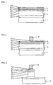
- the production of an extraordinarily narrow base collector mesa 12 (FIG. 9), which extends into the n + sub collector layer 21, is carried out with a photoresist mask.
- a chemically assisted ion beam etching method (CAIBE) is selected for the InP layers 41 and 42, in which a process gas mixture Cl 2 / Ar is used for the removal.
- the InGaAs layers 21, 22, 31 and 32 are removed wet-chemically with a phosphoric acid-hydrogen-peroxide mixture (H 3 PO 4 : H 2 O 2 : H 2 O).
- the subsequent production of a collector-substrate mesa 13, which extends into the substrate 1, serves to isolate the component.
- the collector metal 6 is applied using a photoresist mask.
- a first planarization step is then carried out, in which the semiconductor surface is covered up to the upper limit of the base.
- a first polyimide layer 7 is applied, which is etched back in the oxygen plasma up to the upper limit of the base by means of a reactive ion etching process (RIE).
- RIE reactive ion etching process
- the InP protective layer 41 and 42 is of central importance for the etching back of the polyimide layer 7.
- the InP n emitter layer 41 and the first n + emitter cap layer 42 made of InP are then removed using an etching solution based on hydrochloric acid, and the base metal 8 is applied to the emitter base mesa 11 in a self-adjusting manner immediately thereafter.
- the base metal 8 extends laterally onto the first planarization layer, this in particular being continued as a metal conductor track for making contact via the first polyimide layer 7.
- a second planarization step the semiconductor surface is covered up to the upper limit of the emitter.
- a second polyimide layer 9 is again applied, which is etched back in the oxygen plasma up to the upper limit of the emitter.
- the last process document contains the connection metallization 10 of emitter 4, base 3 and collector 2 by means of reactive ion etching and an electrochemical deposition of gold in the areas provided for this.
- the semiconductor layer sequence can be varied on the basis of the process sequence used according to exemplary embodiment 1.
- the InGaAs intrinsic base spacer layer 32 and / or the first n + emitter cap layer 42 made of InP can also be dispensed with.
- the n-emitter layer 41 and the first n + -emitter cap layer 42 can also consist of InAlAs.
- a second n + emitter cap layer 43 made of InGaAs with a thickness of 20 nm and a doping concentration of approx. 1x10 19 cm -3 can follow on the first n + emitter cap layer 42, the In content in the layer having a gradient between 0% up to 50%.
- an AlGaAs n layer with a gradient in the Al content between 30% to 0% can be used, with a thickness of 30 nm and the doping concentration of approx. 1x10 18 cm -3 .
Landscapes
- Bipolar Transistors (AREA)
Applications Claiming Priority (2)
| Application Number | Priority Date | Filing Date | Title |
|---|---|---|---|
| DE19834491 | 1998-07-31 | ||
| DE19834491A DE19834491A1 (de) | 1998-07-31 | 1998-07-31 | Anordnung und Verfahren zur Herstellung eines Heterobipolartransistors |
Publications (2)
| Publication Number | Publication Date |
|---|---|
| EP0977250A2 true EP0977250A2 (fr) | 2000-02-02 |
| EP0977250A3 EP0977250A3 (fr) | 2000-03-22 |
Family
ID=7875930
Family Applications (1)
| Application Number | Title | Priority Date | Filing Date |
|---|---|---|---|
| EP99114471A Withdrawn EP0977250A3 (fr) | 1998-07-31 | 1999-07-23 | Structure et procédé de fabrication d'un transistor bipolaire à hétérojonction |
Country Status (4)
| Country | Link |
|---|---|
| US (1) | US6365477B1 (fr) |
| EP (1) | EP0977250A3 (fr) |
| JP (1) | JP2000058557A (fr) |
| DE (1) | DE19834491A1 (fr) |
Cited By (3)
| Publication number | Priority date | Publication date | Assignee | Title |
|---|---|---|---|---|
| WO2002103802A3 (fr) * | 2001-06-18 | 2003-02-27 | Epiworks Inc | Transistor a couche de base presentant un desaccord intentionnel de reseau en traction |
| WO2003056629A1 (fr) | 2002-01-03 | 2003-07-10 | Qinetiq Limited | Transistors bipolaires a large bande interdite |
| EP1416539A3 (fr) * | 2002-10-30 | 2005-01-26 | Sharp Kabushiki Kaisha | Transistor bipolaire à hétérojonction |
Families Citing this family (1)
| Publication number | Priority date | Publication date | Assignee | Title |
|---|---|---|---|---|
| US10622465B2 (en) | 2017-12-20 | 2020-04-14 | Qualcomm Incorporated | Heterojunction bipolar transistor (HBT) |
Family Cites Families (19)
| Publication number | Priority date | Publication date | Assignee | Title |
|---|---|---|---|---|
| JP2542676B2 (ja) * | 1987-07-02 | 1996-10-09 | 株式会社東芝 | ヘテロ接合バイポ―ラトランジスタ |
| JPH05243256A (ja) * | 1992-03-02 | 1993-09-21 | Matsushita Electric Ind Co Ltd | ヘテロ接合バイポーラトランジスタおよびその製造方法 |
| JPH0669227A (ja) * | 1992-05-29 | 1994-03-11 | Texas Instr Inc <Ti> | 化合物半導体のヘテロ接合バイポーラトランジスタ及びその製造方法 |
| US5298438A (en) * | 1992-08-31 | 1994-03-29 | Texas Instruments Incorporated | Method of reducing extrinsic base-collector capacitance in bipolar transistors |
| JPH06132298A (ja) * | 1992-10-14 | 1994-05-13 | Mitsubishi Electric Corp | 半導体装置の製造方法 |
| US5571732A (en) * | 1993-08-19 | 1996-11-05 | Texas Instruments Incorporated | Method for fabricating a bipolar transistor |
| US5468659A (en) * | 1994-03-10 | 1995-11-21 | Hughes Aircraft Company | Reduction of base-collector junction parasitic capacitance of heterojunction bipolar transistors |
| US5445976A (en) * | 1994-08-09 | 1995-08-29 | Texas Instruments Incorporated | Method for producing bipolar transistor having reduced base-collector capacitance |
| US5702958A (en) * | 1994-08-09 | 1997-12-30 | Texas Instruments Incorporated | Method for the fabrication of bipolar transistors |
| JPH08181151A (ja) * | 1994-12-26 | 1996-07-12 | Mitsubishi Electric Corp | バイポーラトランジスタ |
| EP0817276A4 (fr) * | 1995-03-17 | 1998-08-19 | Hitachi Ltd | Dispositif a semi-conducteur et son procede de production |
| US5665614A (en) * | 1995-06-06 | 1997-09-09 | Hughes Electronics | Method for making fully self-aligned submicron heterojunction bipolar transistor |
| JPH09162194A (ja) * | 1995-12-08 | 1997-06-20 | Mitsubishi Electric Corp | ヘテロ接合バイポーラトランジスタ |
| DE19609933A1 (de) * | 1996-03-14 | 1997-09-18 | Daimler Benz Ag | Verfahren zur Herstellung eines Heterobipolartransistors |
| US5736417A (en) * | 1996-05-13 | 1998-04-07 | Trw Inc. | Method of fabricating double photoresist layer self-aligned heterojunction bipolar transistor |
| US5625206A (en) * | 1996-06-03 | 1997-04-29 | Lucent Technologies Inc. | High-speed double-heterostructure bipolar transistor devices |
| US5656515A (en) * | 1996-07-18 | 1997-08-12 | Lucent Technologies, Inc. | Method of making high-speed double-heterostructure bipolar transistor devices |
| JP3347947B2 (ja) * | 1996-08-01 | 2002-11-20 | 日本電信電話株式会社 | 半導体装置の製造方法 |
| US5907165A (en) * | 1998-05-01 | 1999-05-25 | Lucent Technologies Inc. | INP heterostructure devices |
-
1998
- 1998-07-31 DE DE19834491A patent/DE19834491A1/de not_active Ceased
-
1999
- 1999-07-23 EP EP99114471A patent/EP0977250A3/fr not_active Withdrawn
- 1999-07-30 US US09/363,746 patent/US6365477B1/en not_active Expired - Fee Related
- 1999-08-02 JP JP11219229A patent/JP2000058557A/ja active Pending
Cited By (4)
| Publication number | Priority date | Publication date | Assignee | Title |
|---|---|---|---|---|
| WO2002103802A3 (fr) * | 2001-06-18 | 2003-02-27 | Epiworks Inc | Transistor a couche de base presentant un desaccord intentionnel de reseau en traction |
| WO2003056629A1 (fr) | 2002-01-03 | 2003-07-10 | Qinetiq Limited | Transistors bipolaires a large bande interdite |
| EP1416539A3 (fr) * | 2002-10-30 | 2005-01-26 | Sharp Kabushiki Kaisha | Transistor bipolaire à hétérojonction |
| US7030462B2 (en) | 2002-10-30 | 2006-04-18 | Sharp Kabushiki Kaisha | Heterojunction bipolar transistor having specified lattice constants |
Also Published As
| Publication number | Publication date |
|---|---|
| DE19834491A1 (de) | 2000-02-03 |
| JP2000058557A (ja) | 2000-02-25 |
| US6365477B1 (en) | 2002-04-02 |
| EP0977250A3 (fr) | 2000-03-22 |
Similar Documents
| Publication | Publication Date | Title |
|---|---|---|
| DE69605718T2 (de) | Völlig selbstjustierter Submikrometer-Bipolartransistor mit einem Heteroübergang und Verfahren zu dessen Herstellung | |
| DE3788527T2 (de) | Bipolarer Transistor und sein Herstellungsverfahren. | |
| DE69621088T2 (de) | Bipolartransistor und Verfahren zur Herstellung | |
| EP0005728A1 (fr) | Procédé de fabrication d'un transistor latéral PNP ou NPN à haut gain et transistor obtenu | |
| DE112012000611T5 (de) | Siliziumkarbid-Bipolartransistor mit Abschirmbereichen und Verfahren zu dessen Herstellung | |
| DE69524516T2 (de) | Verfahren zur Herstellung eines Bipolatransistors | |
| EP0293641A1 (fr) | Procédé de fabrication à un transistor bipolaire entièrement auto-aligné | |
| DE60036729T2 (de) | Heteroübergang-Bipolartransistor mit obenliegendem Kollektor und dessen Herstellungsverfahren | |
| JP2536523B2 (ja) | 半導体装置の製造方法 | |
| DE69128123T2 (de) | Verfahren zum Herstellen selbst-ausrichtender bipolarer Transistoren mit Heteroübergang | |
| DE3936507C2 (de) | Selbstjustierter Bipolartransistor mit Heteroübergang und Verfahren zur Herstellung desselben | |
| DE4014216C2 (de) | Verfahren zum Herstellen eines Hetero-Bipolar-Transistors | |
| DE3871928T2 (de) | Verfahren zur herstellung eines bipolaren heterouebergangstransistor. | |
| DE3686253T2 (de) | Herstellung einer halbleitervorrichtung mit eingebettetem oxyd. | |
| DE102015204411B4 (de) | Transistor und Verfahren zur Herstellung eines Transistors | |
| DE69220830T2 (de) | Verfahren zur Herstellung von Halbleietervorrichtungen | |
| DE69315813T2 (de) | Kaskodenschaltungsstruktur mit bipolaren Epitoxial-Transistoren und niedrig gelegenem Basisanschluss | |
| EP0977250A2 (fr) | Structure et procédé de fabrication d'un transistor bipolaire à hétérojonction | |
| DE10124032B4 (de) | Verfahren zur Herstellung von Bauelementen auf einem SOI-Wafer | |
| EP1354342A2 (fr) | Procede pour fabriquer un composant semi-conducteur comportant une electrode de contact en forme de t | |
| EP0460285B1 (fr) | Procédé de fabrication d'un transistor bipolaire ayant une capacité base-collecteur extrêmement réduite | |
| EP0416166B1 (fr) | Méthodes de fabrication d'un transistor bipolaire à hétérojonction et à contact de collecteur séparé | |
| DE3888602T2 (de) | Bipolartransistor mit Heteroübergängen. | |
| DE3785837T2 (de) | Verfahren zur herstellung eines iii-v-halbleiterbauelementes. | |
| DE3620686C2 (de) | Strukturierter Halbleiterkörper |
Legal Events
| Date | Code | Title | Description |
|---|---|---|---|
| PUAI | Public reference made under article 153(3) epc to a published international application that has entered the european phase |
Free format text: ORIGINAL CODE: 0009012 |
|
| AK | Designated contracting states |
Kind code of ref document: A2 Designated state(s): DE FR GB |
|
| AX | Request for extension of the european patent |
Free format text: AL;LT;LV;MK;RO;SI |
|
| PUAL | Search report despatched |
Free format text: ORIGINAL CODE: 0009013 |
|
| RTI1 | Title (correction) |
Free format text: STRUCTURE AND PROCESS FOR THE FABRICATION OF A HETEROJUNCTION BIPOLAR TRANSISTOR |
|
| AK | Designated contracting states |
Kind code of ref document: A3 Designated state(s): AT BE CH CY DE DK ES FI FR GB GR IE IT LI LU MC NL PT SE |
|
| AX | Request for extension of the european patent |
Free format text: AL;LT;LV;MK;RO;SI |
|
| RTI1 | Title (correction) |
Free format text: STRUCTURE AND PROCESS FOR THE FABRICATION OF A HETEROJUNCTION BIPOLAR TRANSISTOR |
|
| 17P | Request for examination filed |
Effective date: 20000411 |
|
| AKX | Designation fees paid |
Free format text: DE FR GB |
|
| RAP1 | Party data changed (applicant data changed or rights of an application transferred) |
Owner name: UNITED MONOLITHIC SEMICONDUCTORS GMBH |
|
| 17Q | First examination report despatched |
Effective date: 20061006 |
|
| STAA | Information on the status of an ep patent application or granted ep patent |
Free format text: STATUS: THE APPLICATION IS DEEMED TO BE WITHDRAWN |
|
| 18D | Application deemed to be withdrawn |
Effective date: 20070217 |